Present Address: ]Los Alamos National Laboratory Present Address: ]Griffith University, Brisbane, Australia Present Address: ]University of Ulm, Germany
A microfabricated surface-electrode ion trap in silicon
Abstract
The prospect of building a quantum information processor underlies many recent advances ion trap fabrication techniques. Potentially, a quantum computer could be constructed from a large array of interconnected ion traps. We report on a micrometer-scale ion trap, fabricated from bulk silicon using micro-electromechanical systems (MEMS) techniques. The trap geometry is relatively simple in that the electrodes lie in a single plane beneath the ions. In such a trap we confine laser-cooled 24Mg+ ions approximately 40 m above the surface. The fabrication technique and planar electrode geometry together make this approach amenable to scaling up to large trap arrays. In addition we observe that little laser cooling light is scattered by the electrodes.
pacs:
32.80.PjTrapped ions are an attractive system for large scale quantum information processing (QIP) Cirac and Zoller (2000); ard . All the building blocks of such a processor are demonstrated in the laboratory, and there is no known fundamental obstacle to scaling up to a large processor. Nevertheless considerable challenges remain, including methods of manipulating large arrays of ion qubits. Some proposed schemes for QIP in ions involve many interconnected ion traps with integrated optics and control electronics DeVoe (1998); Wineland et al. (1998); Cirac and Zoller (2000); Kielpinski et al. (2002); Duan et al. (2004); Kim et al. (2005). This paper describes a new approach for making trap structures that is relatively straightforward and holds the potential of scaling up.
A straightforward implementation of a linear radio-frequency (RF) ion trap consists of four parallel conducting rods as depicted in Figure 2(a) Paul (1990). With opposite pairs of rods held at RF-ground and RF potential respectively, a ponderomotive potential arises that provides nearly harmonic confinement in the - radial plane, as in a RF quadrupole mass filter. The RF-grounded rods can be segmented (as illustrated) and a static positive potential (for positive ions) is applied to the end segments relative to the inner segments Raizen et al. (1993). This defines a trap zone for charged particles in the axial direction. This type of trap has been used in ion QIP work but may be difficult to implement on a large scale. Key trap characteristics for large arrays of qubits include a small ion-electrode spacing, accurately defined smooth electrode surfaces, low RF losses, compatibility with on-chip control electronics, a low anomalous heating rate Turchette et al. (2000); Wineland et al. (1998); Chiaverini et al. (2005); Deslauriers et al. (2006), and the possibility of scaling to many trapping zones Wineland et al. (2005a); Kim et al. (2005). No current trap technology meets all these requirements.
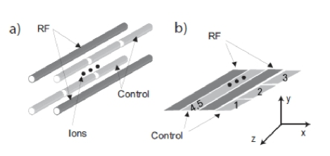
Among several RF ion-trap electrode configurations Schrama et al. (1993); Raizen et al. (1993); Ghosh (1995); Rowe et al. (2002); Blain et al. (2004); Home and Steane (2004); Barrett et al. (2004); Wineland et al. (2005b); Hensinger et al. (2006); Stick et al. (2006); Seidelin et al. (2006); Brown et al. (2006), two approaches have emerged as possible candidates for scaling to large arrays of traps. One approach uses multilayered structures with large trap depths and open optical access but which are relatively difficulty to fabricate because of the number of layers Rowe et al. (2002); Home and Steane (2004); Barrett et al. (2004); Wineland et al. (2005b); Hensinger et al. (2006); Stick et al. (2006). Two microfabricated multilayer traps have been demonstrated: in boron-doped silicon Wineland et al. (2005b) and in aluminum-gallium-arsenide Stick et al. (2006). Alternately, single-layer traps, wherein all electrodes lie in a single plane, are more amenable to microfabrication and integration with on-chip control electronics Chiaverini et al. (2005); Kim et al. (2005), see Figure 2b. Recently this approach was demonstrated for atomic ions in a trap with gold electrodes on a fused silica substrate Seidelin et al. (2006) and with copper electrodes on a GML-1000 printed circuit board Brown et al. (2006).
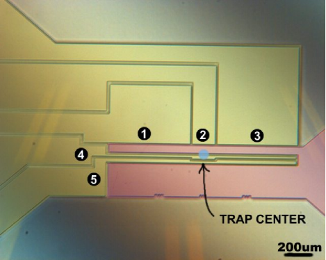
Here we report on the demonstration of a different fabrication technique for surface-electrode traps where the electrodes are lithographically defined from the bulk of a silicon wafer. While the geometry is similar to that in Seidelin et al. (2006), the fabrication method described here has several advantages: the process uses only silicon, so it is compatible with CMOS foundry processes Kim et al. (2005); surfaces exposed to the ion have low surface roughness ( nm RMS); and stray fields from insulators are minimized since the trapping region lies far from the nearest insulating surface, see Figures 1,3, and 4. Using this technology, multizone traps with electrodes m wide are practical.
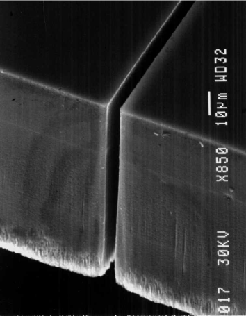
A demonstration trap was fabricated by through-wafer etching of a commercially available boron doped silicon wafer. The electrode pattern was defined by standard photolithography, then etched using deep reactive ion etching (DRIE), a standard MEMS technique also known as the Bosch process Bhardwaj and Ashraf (1995); Madou (1997). This etch can produce trenches of arbitrary lateral geometry, hundreds of micrometers deep and as small as several micrometers wide while maintaining an etch aspect ratio of and low sidewall roughness, see Figure 4. The commercially available silicon is doped with boron as the silicon crystal is grown yielding resistivities of ohm-cm; no additional metalization is needed in the trap region. For reference, at room temperature Au ohm-cm, Ti ohm-cm and W ohm-cm Lide (2006).
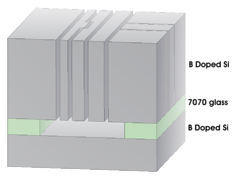
After etching, structural support is provided by anodic bonding of the silicon wafer to a glass substrate Tong and Gösele (1998); Kielpinski (2001). The glass has a gap beneath the trapping region above which the silicon electrodes are cantilevered in vacuum, see Figure 4. This gap is present to keep dielectric surfaces away from the trap region and to reduce the penetration of RF fields into the glass. The glass is a borosilicate () with a loss tangent of ( MHz, C) and a coefficient of thermal expansion (CTE) matched to silicon. For reference, the loss tangent of Pyrex () is and that of pure alumina is cor .
The anodic bonding is done after thorough cleaning to remove organic contaminants and the native silicon oxide by use of solutions of : :: H2SO4 : H2O2 at C and : :: % NH4F : %HF at C, respectively. The etch geometry is arranged so that all the electrodes are joined at the periphery until after bonding, whereupon they are separated by a perpendicular cut with a dicing saw Kielpinski (2001). For wiring to external leads, contact pads are made by evaporative deposition of Ti and Cu near the periphery of the chip.
The electrode geometry used here is shown in Figure 1. Five independent static-potential control electrodes are present in this design. The control electrodes define the axial potential curvature and provide sufficient degrees of freedom to properly overlap the static electric field with the RF pseudopotential minimum, that minimizes ion micromotion in both radial directions Chiaverini et al. (2005); Seidelin et al. (2006).
Capacitive coupling of the RF and control electrodes due to their close proximity can induce an undesirable RF potential on the latter; this is minimized by coupling the control electrodes to ground through low-pass RC filters mounted on a ceramic chip carrier within the vacuum housing Rowe et al. (2002).
Ions are created by laser photoionization (PI) of an atomic vapor evolved from a resistively heated ampule containing 24Mg. In some trap designs there is risk of this vapor causing shorts between trap electrodes Pearson et al. (2005); Seidelin et al. (2006); Brown et al. (2006); the cantilevered geometry avoids this problem as vacuum separates the electrodes in the trapping region. For PI a laser is tuned to the 3sS0 3s3p 1P1 electric dipole transition in neutral magnesium at nm Madsen et al. (2000); Madsen and Thomsen (2002). From the 3s3p 1P1 state, absorption of another photon at nm can excite the electron to the continuum. The PI beam is present in the trap region only during the loading phase.
The ions are Doppler cooled with a nm laser tuned MHz red of the 3s 2S1/2 3p 2P electric-dipole transition in 24Mg+. The laser beam propagates parallel to the trap surface, at an angle of with respect to the trap -axis, see Figures 1 and 2b. The radial trap axes lie at approximately with respect to the trap surface. Therefore, the laser has a projection along all three axes, allowing laser cooling along all axes Chiaverini et al. (2005).
The cooling and PI beams copropagate. They have a power of W and W respectively, measured after they exit the vacuum apparatus. At the trapping region they have a waist of approximately m and are centered approximately m above the surface. Ions are detected by observing the ion fluorescence on a CCD camera. The background includes stray light scattered from the cooling laser beam by the apparatus. The signal-to-background for a single ion is higher than even with a beam intensity times the resonance saturation intensity, limited by noise due to the CCD chip.
Initial trap parameters (RF and control electrode potentials) were determined numerically by the boundary element method. The primary solution constraint is that the micromotion be nulled as discussed above. An ion was first trapped with static potentials of , , , and volts and estimated peak RF potential of amplitude with respect to DC ground at MHz. For these parameters the expected trap depth is approximately meV, and the ions are located m above the surface. Figure 5 shows a linear crystal of three ions trapped using these potentials.
The axial oscillation frequency was measured experimentally by applying oscillating potentials to electrode . When resonant with a motional mode of the ions, the motion is excited. We detect this by observing a change in the ion’s fluorescence due to Doppler broadening Jefferts et al. (1995). With the trap parameters listed above, for three ions an axial frequency of kHz was measured. Figure 6 shows a linear crystal of twelve ions achieved by lowering the axial potential on the endcaps to mV, mV and mV. This configuration holds the ions in a linear chain due to a relatively strong axial component of the RF pseudopotential. Single ion lifetimes greater than one hour were observed.


Heating of the ion motion is a concern in all ion traps and is an important consideration in evaluating new fabrication techniques Monroe et al. (1995); Wineland et al. (1998); Turchette et al. (2000); Deslauriers et al. (2006) for QIP. Therefore, the next steps in the evaluation of this trap will include characterization of the heating at the quantum level.
It is important to investigate a variety of approaches to ion trap fabrication on the way towards larger QIP processors. Particular attention must be paid to the practicality of scaling to many trapping zones and to material science issues raised by anomalous heating.
This work was supported by the Advanced Research and Development Activity (ARDA) under contract and NIST. S. S. thanks the Carlsberg Foundation for financial support; J. H. W. thanks the Danish Research Agency. This manuscript is a publication of NIST and not subject to U.S. copyright.
References
- Cirac and Zoller (2000) J. I. Cirac and P. Zoller, Nature 404, 579 (2000).
- (2) eprint See for instance http://qist.lanl.gov/.
- DeVoe (1998) R. G. DeVoe, Phys. Rev. A 58, 910 (1998).
- Wineland et al. (1998) D. J. Wineland, C. Monroe, W. M. Itano, D. Leibfried, B. E. King, and D. M. Meekhof, J. Res. Nat. Inst. Stand. Tech. 103, 259 (1998).
- Kielpinski et al. (2002) D. Kielpinski, C. Monroe, and D. J. Wineland, Nature 417, 709 (2002).
- Duan et al. (2004) L. M. Duan, B. B. Blinov, D. L. Moehring, and C. Monroe, Quant. Inform. Comp. 4, 165 (2004).
- Kim et al. (2005) J. Kim, S. Pau, Z. Ma, H. R. McLellan, J. V. Gates, A. Kornblit, R. E. Slusher, R. M. Jopson, I. Kang, and M. Dinu, Quant. Inform. Comp. 5, 515 (2005).
- Paul (1990) W. Paul, Rev. Mod. Phys. 62, 531 (1990).
- Raizen et al. (1993) M. G. Raizen, J. M. Gilligan, J. C. Bergquist, W. M. Itano, and D. J. Wineland, Phys. Rev. A 45, 6493 (1993).
- Turchette et al. (2000) Q. A. Turchette, D. Kielpinski, B. E. King, D. Leibfried, D. M. Meekhof, C. J. Myatt, M. A. Rowe, C. A. Sackett, C. S. Wood, W. M. Itano, et al., Phys. Rev. A 61, 063418 (2000).
- Chiaverini et al. (2005) J. Chiaverini, R. B. Blakestad, J. Britton, J. D. Jost, C. Langer, D. Leibfried, R. Ozeri, and D. J. Wineland, Quant. Inform. Comp. 5, 419 (2005).
- Deslauriers et al. (2006) L. Deslauriers, S. Olmschenk, D. Stick, W. K. Hensinger, J. Sterk, and C. Monroe, quant-ph/0602003 (2006).
- Wineland et al. (2005a) D. J. Wineland, C. Monroe, R. Blatt, and A. Steane (2005a), eprint http://www.nbc.gov/trap_specifications_v3.pdf.
- Schrama et al. (1993) C. A. Schrama, E. Peik, W. W. Smith, and H. Walther, Opt. Commun. 101, 32 (1993).
- Ghosh (1995) P. K. Ghosh, Ion Traps (Clarendon Press, Oxford, 1995).
- Rowe et al. (2002) M. A. Rowe, A. Ben-Kish, B. DeMarco, D. Leibfried, V. Meyer, J. Beall, J. Britton, J. Hughes, W. M. Itano, B. Jelenković, et al., Quant. Inform. Comp. 2, 257 (2002).
- Blain et al. (2004) M. G. Blain, L. S. Riter, D. Cruz, D. E. Austin, G. Wu, W. R. Plass, and R. G. Cooks, Int. J. Mass Spect. 236, 91 (2004).
- Home and Steane (2004) J. P. Home and A. M. Steane, quant-ph/0411102 (2004).
- Barrett et al. (2004) M. D. Barrett, J. Chiaverini, T. Schaetz, J. Britton, W. M. Itano, J. D. Jost, E. Knill, C. Langer, D. Leibfried, R. Ozeri, et al., Nature 429, 737 (2004).
- Wineland et al. (2005b) D. J. Wineland, D. Leibfried, M. D. Barrett, A. Ben-Kish, J. C. Bergquist, R. B. Blakestad, J. J. Bollinger, J. Britton, J. Chiaverini, B. DeMarco, et al., in Laser Spectroscopy, Proc. XVII Int. Conf. on Laser Spectroscopy, Avemore, Scotland, edited by E. A. Hinds, A. Ferguson, and E. Riis (World Scientific, Singapore, 2005b), pp. 393–402.
- Hensinger et al. (2006) W. K. Hensinger, S. Olmschenk, D. Stick, D. Hucul, M. Yeo, M. Acton, L. Deslauriers, C. Monroe, and J. Rabchuk, Appl. Phys. Lett. 88, 034101 (2006).
- Stick et al. (2006) D. Stick, W. K. Hensinger, S. Olmschenk, M. J. Madsen, K. Schwab, and C. Monroe, Nature Physics 2, 36 (2006).
- Seidelin et al. (2006) S. Seidelin, J. Chiaverini, R. Reichle, J. J. Bollinger, D. Leibfried, J. Britton, J. H. Wesenberg, R. B. Blakestad, R. J. Epstein, D. B. Hume, et al., quant-ph/0601173 (2006).
- Brown et al. (2006) K. R. Brown, R. J. Clark, J. Labaziewicz, P. Richerme, D. R. Leibrandt, and I. L. Chuang, ”quant-ph/0603142” (2006).
- Bhardwaj and Ashraf (1995) J. K. Bhardwaj and H. Ashraf, Proceedings of Micromachining and Microfabrication Process Technology Symposium of the International Society for Optical Engineering, Austin, Texas (1995).
- Madou (1997) M. Madou, Fundamentals of Microfabrication (CRC Press, New York, 1997), 1st ed.
- Lide (2006) D. R. Lide, CRC Handbook of Chemistry and Physics (Taylor and Francis, Boca Raton, L, 2006), 86th ed.
- Tong and Gösele (1998) Q. Y. Tong and U. Gösele, Semiconductor wafer bonding science and technology (Wiley-Interscience, 1998), 1st ed.
-
Kielpinski (2001)
D. Kielpinski, Ph.D. thesis,
Univ. Colorado, Dept. of Physics, Boulder
(http://tf.nist.gov/
ion/qucomp/papers/dkthesis/dkthesis.pdf) (2001). - (30) eprint See http://www.corning.com/lightingmaterials/images /wafersheet.pdf.
- Pearson et al. (2005) C. E. Pearson, D. R. Leibrandt, W. S. Bakr, W. J. Mallard, K. R. Brown, and I. L. Chuang, ”quant-ph/0511018” (2005).
- Madsen et al. (2000) D. N. Madsen, S. Balslev, M. Drewsen, N. Kjærgaard, Z. Videsen, and J. W. Thomsen, J. Phys. B 33, 4981 (2000).
- Madsen and Thomsen (2002) D. N. Madsen and J. W. Thomsen, J. Phys. B 35, 2173 (2002).
- Jefferts et al. (1995) S. R. Jefferts, C. Monroe, E. W. Bell, and D. J. Wineland, Phys. Rev. A 51, 3112 (1995).
- Monroe et al. (1995) C. Monroe, D. M. Meekhof, B. E. King, W. M. Itano, and D. J. Wineland, Phys. Rev. Lett. 75, 4714 (1995).