Design and Operation of Front-End Electronics for the HERA-B Muon Detector
Abstract
We have implemented a cost-effective design for the readout electronics of both the anode wires and the cathode pads of large area proportional wire chambers for the HERA-B muon system based on the ASD-08 integrated circuit. To control and monitor the large number of readout channels, we have built a distributed control system based on Philips Semiconductors’ I2C bus and microcontrollers. To date we have installed about 10800 channels of muon chambers and electronics. The average single channel noise occupancy is less than , and the detectors have been operated with target interaction rates as high as 70 MHz.
©1998 IEEE. Personal use of this material is permitted. However, permission to reprint/republish this material for advertising or promotional purposes or for creating new collective works for resale or redistribution to servers or lists, or to reuse any copyrighted component of this work in other works must be obtained from the IEEE.
This material is presented to ensure timely dissemination of scholarly and technical work. Copyright and all rights therein are retained by authors or by other copyright holders. All persons copying this information are expected to adhere to the terms and constraints invoked by each author’s copyright. In most cases, these works may not be reposted without the explicit permission of the copyright holder.
I Introduction
The HERA-B experiment at DESY is designed to observe and measure CP violation in B decays. Precise CP violation measurements will either provide an accurate determination of the values of the CKM matrix or will point to new physics beyond the Standard Model. In the HERA-B experiment, HERA’s 820 GeV circulating proton beam interacts with a wire target placed in the beam’s halo. The proton-nucleus interactions copiously produce B events which must be culled from the large non-B background. This places great importance on triggering and event selection. For B decays, this means identification of non-prompt J/ decays and leptons with high transverse momentum. Hence, the muon detector plays a primary role in particle identification and triggering in the experiment.
The muon system is segmented into 4 large superlayers, which measure roughly 6 m 8 m. The 4 superlayers are interleaved with iron-loaded concrete to screen out hadrons, and they are located in the region from about 16 m to 20 m downstream of the target. The system covers angles from about 10 mrad near the beam pipe up to maximum angles of 160 mrad vertically (in y) and of 220 mrad horizontally (in the bend plane or x-direction). The entire system consists of about 32000 channels of readout. Figure 1 shows a view of the entire muon system.
Three kinds of detectors make up the muon system: tube chambers, pad chambers, and pixel chambers. The tube and pad chambers are closed-cell proportional wire chambers. The cell dimensions are mm2. About 15000 anode wires and 8000 cathode pads in these chambers cover angles from about 50 mrad up to the maximum angles in x and y. The first two superlayers consist of tube chambers arranged into 3 stereo views. The wire angles are and with respect to the vertical. Superlayers 3 and 4 consist of pad chambers arranged only into the view. Each superlayer also has a pixel system that makes up about 9000 channels in the muon system. The pixel chambers cover the small angles from 10-50 mrad near the beam line.
The tube and pad chambers each have two layers of 16 anode wires of pitch 16 mm; one layer is offset by 1/2 cell from the other layer. The chamber width is 262 mm, and the lengths vary; a typical length is approximately 3 m. The anode wires are made of gold-plated tungsten of diameter 45 m. Inside each pad chamber are two copper clad phenolic boards. Sixty cathode pads (2 columns of 30) of approximate size mm2 are cut into the copper cladding of each phenolic board. The boards are mounted inside the pad chamber so that the pads in the two layers are aligned. Figure 2 shows superlayer 1, the first completed superlayer, before insertion into the muon absorber. For more information on the construction and geometry of the muon chambers, see references [1] and [2].
II Front End Electronics
A Choice of Front End Device
The HERA-B spectrometer contains several large systems requiring high gain, front-end amplifiers with discriminated (yes/no) readout. These systems are the large angle drift chamber tracking system (96000 channels), the muon detector (32000 channels), the detectors for the high transverse momentum trigger (26000 channels), and the ring imaging Cherenkov (RICH) detector (28000 channels). The large number of channels dictated the need for a cost effective solution that would be usable in all systems. All the detectors mentioned above, except for the RICH phototubes, employ gas avalanche techniques. The high bunch crossing rate at HERA-B (10 MHz) makes desirable the highest possible electronic gain in the front end amplifiers. This allows these detectors to operate at the lowest possible avalanche gain.
An attractive solution is the ASD-08 integrated circuit [3] developed for the straw tube drift chamber tracker for the Solenoid Detector Collaboration at the Superconducting Super Collider. In the muon tube chambers, for example, at nominal high voltage of 2.3 kV, a minimum ionizing particle produces an anode signal with a mean value of about 30 fC within the 7 ns shaping time of the ASD-08. Using a digital storage oscilloscope, this was determined by direct measurement of anode pulses from cosmic rays. This matches perfectly with the fC level thresholds which the ASD-08 allows. Packaged chips were produced in large quantities for HERA-B in 1997 for $2.34 per channel, not including testing. The wafers were fabricated by MAXIM Microelectronics (Beaverton, Oregon) and packaged by Hana Technologies (Hong Kong).
B Anode Wire Front End Electronics
The front end electronics for reading out the anode wires are implemented on 32-channel, printed circuit boards (“tube cards”, for short). The size is roughly mm2. They are mounted in close proximity to the anode wire feedthroughs of the tube and pad chambers. Figure 3 shows one such card mounted on a tube chamber. Each anode wire is connected to the card via a short (approx. 6 cm), insulated wire. The wire is rated for 18 kV (from Reynolds Industries, Los Angeles, California). It is soldered to the feedthrough at one end and has a single pin connector at the card end. The wire is kept as short as possible to minimize electromagnetic pickup to the amplifier input.
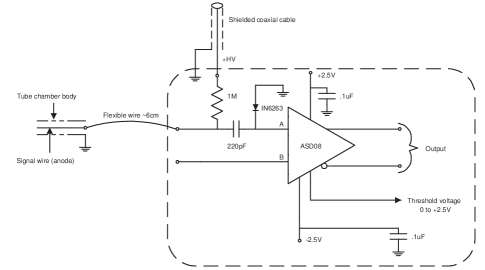
A schematic diagram of the input stage from anode wire to ASD-08 appears in Figure 4. The high voltage distribution resistors (1 M) are located on the same PCB as the ASD-08 package. The high voltage is provided via an HTC-50-1-1, miniature coaxial cable. This flexible cable has an outer diameter of 3.3 mm. An internal discharge shield allows operation up to 5 kV. The high voltage is blocked from the ASD-08 by a 220 pF ceramic, wire-lead capacitor rated at 6 kV (XICON Passive Components, Arlington, Texas). All other components are of the surface mount type. To protect against air discharges, the board is spray coated with a clear insulating varnish, Krylon 7001. A Schottky-barrier diode, type 1N6263, protects the ASD-08 if a discharge occurs in the chamber between the anode wire and ground. In this case, the capacitor discharge current will flow through the diode.
The design of the tube card includes a number of features to reduce electromagnetic pickup of noise and to increase the impedance of feedback paths. Input and output traces of the ASD-08 are sandwiched between ground and power planes of the circuit board. Overall, the printed circuit board has 5 layers. The ASD-08 has differential inputs; one is connected to an anode wire, and the other is connected to a parallel trace equal in length. This allows for differential cancellation of noise pickup along the input trace path. Decoupling capacitors (0.1 F) are located near the ASD-08 package at the bias pins. Also, 10 F capacitors filter the bias voltages (-2.5 V and +2.5 V) near the power input connector.
The ASD output drives long (up to 20 m), twisted-pair signal cables. The signal cables plug into a module termed the Front End Driver (FED) by HERA-B. It is a custom module built commercially for HERA-B by MSC (Stutensee, Germany). The FED pulls up the differential output lines of the ASD by terminating them through 62 into +1.6 V. The FED latches the ASD data and holds it in a 128 event deep buffer while the pretrigger and the first level trigger decide whether the data is worthy of sending to the second level trigger.
C Cathode Pad Front End Electronics
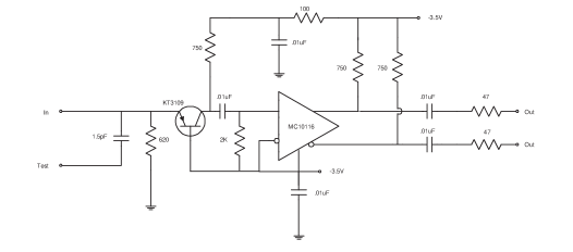
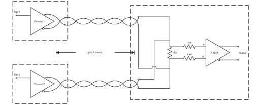
The large length of the muon pad chambers ( m) and need to transport the cathode signals over large distances requires that the front end electronics be separated into two stages. The first stage is a preamplifier. It is mounted near the cathode pads, inside the pad chambers, and on the side of the phenolic board opposite to the anode wires. Each preamplifier board is roughly mm2 and provides preamplification for 3 cathode pads. Two bus lines cut into the copper cladding of the phenolic boards supply power (-3.5 V) and ground to the preamplifiers.
The schematic for one such preamp channel appears in Figure 5. The input stage of the preamplifier circuit consists of a KT3109 transistor in common base configuration. This allows a small input impedance to the preamplifier circuit. The output stage consists of an ECL Line driver (MC10116 by Motorola). It drives long ( m) twist-and-flat cables from near the cathode pad to the input of the readout electronics located at the end of the chamber. The overall gain of the preamplifier is approximately 1.2 mV/A. To reduce the number of readout channels, a pad from one phenolic board is OR’d with a pad from the other board. Figure 7 shows the OR-ing of the two pads.
The cathode pad front end card (“pad card”) is implemented as a 5-layer printed circuit board of dimensions mm2. Figure 6 shows the top and bottom sides of the pad card. The input portion of the pad card contains a termination and voltage divider network. The network terminates the cables and attenuates the large signal from the preamplifier into the range expected by the ASD. This allows us to use the ASD integrated circuit in this application. After this network, the inverting and noninverting outputs from the driving stage of the preamplifier feed into the A and B inputs, respectively, of the ASD-08.
D Test and Calibration Procedures
We receive untested ASD-08 chips from the manufacturer. Our first task is to test them before mounting them on boards. For this test, channel thresholds are set to 360 mV, and through a 1 pF capacitor, each channel receives an input pulse of approximately 8 fC of charge. The output from the ASD goes to a custom receiver module via twisted pair cables. The receiver module provides the pullup voltage to the ASD output lines, and it converts the ASD signals to NIM levels for observation on an oscilloscope. Under these conditions, a channel is “good” if it gives a pulse of 10-20 ns in width with few noise pulses. About 75% of the chips pass this initial test.
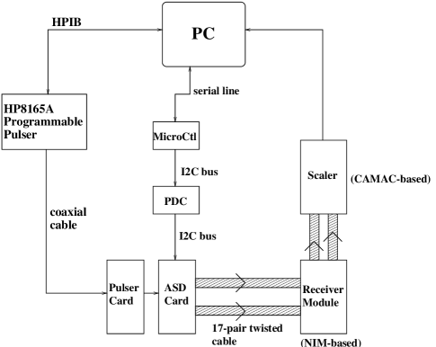
After assembly, each board undergoes a test and calibration of all 32 channels. We constructed a test stand to automate the process. The test stand consists of the apparatus shown in Figure 8. The basic idea of the test is to measure the efficiency of a channel as a function of 2 parameters, injected charge and threshold voltage. A test program on the PC controls a pulser (HP8165A) through an HPIB interface. The program varies the height of a rectangular pulse that the pulser injects into a passive, RC differentiator network; this varies the spike of charge injected into the ASD. Our custom receiver module converts the ASD output to ECL levels which go to a CAMAC-based scaler for counting.
Testing is done in two parts to avoid cross-talk between neighboring channels. For a given pulse height and threshold voltage, the pulser sends 105 pulses to the 16 odd channels on the ASD card. The efficiency is the number of pulses counted by the scaler divided by the 105 injected pulses. The test program scans the efficiency at 10 different pulse heights before changing the threshold. After the odd channels are tested, the operator manually switches the input pulse to the even channels so that they can be tested in the same way. Figure 9 shows the efficiency curves for a good channel of a pad ASD card.
The last step in the testing procedure is to extract the calibration curve from the efficiency data. The filled circles in Figure 9 are the data derived from the efficiency curves. They are the values of the threshold voltage for which the channel is 50% efficient at each value of the injected charge. The test program fits this data to the form: . is the injected charge, and is the threshold voltage at which the channel is 50% efficient; the dotted line shows the calibration curve. As a final step for each channel, the program saves the fit parameters in an EEPROM located on the ASD card. This allows for setting the threshold in terms of a charge threshold rather than a voltage threshold.

The final tests of the ASD cards are done after mounting them onto the chambers. The first test is simply to reduce the threshold enough so that the channel is on 100% of the time. The second test is to turn off the channel by increasing the threshold. This test relies on the highly nonlinear behavior of the threshold above threshold voltages of about 1.1-1.2 V. The charge input required for 50% efficiency increases dramatically for voltages above these values. The channel can easily be switched off by setting the threshold voltage high enough. Lastly, a working channel must have a noise level less than a few 10-4 in the neighborhood of a threshold of 0.8 V (about 4 fC injected charge).
III Power Distribution and Control System
A General Design Overview
With so many front end channels in the muon system, monitoring and controlling them is an important consideration in properly running the apparatus. Providing one threshold voltage per card (32 channels) would be easier than segmenting the threshold voltages further. However, the optimum threshold voltage varies with the ASD channel. The way to maintain the most uniform hit detection efficiency is to provide one threshold voltage per ASD channel. Furthermore, control of individual thresholds allows for setting patterns of on or off channels for trigger testing. Therefore, each front end electronics card contains one 8-channel digital-to-analog converter (DAC) per ASD-08 chip, for a total of 4 DACs per electronics card. To store default threshold values and the threshold calibration per channel, each front end electronics card also contains an EEPROM.
The front end cards (ASD cards) and all their control electronics form a hierarchy from a computer at the highest level to the front end cards at the lowest level, as evident from Figure 10. On the test bench, at the highest level is a PC running under the Windows OS. In the experiment, the highest level is a VME-based Cetia CPU Module, running under the Lynx OS. The computer communicates with a given network of microcontroller cards through a serial port connected to roughly 50 m of cable. Attached to each microcontroller card by cables of approximately 1-3 meters in length are up to 4 power distribution cards. Each power distribution card fans out low voltage power to a maximum of 4 front end cards and acts as a control gateway to them. Therefore, a single microcontroller card controls up to 16 front end cards. Because the muon system is so large, the microcontroller and power distribution cards are distributed along the support frame, near the front end electronics.

B The Microcontroller Card
The intelligence in the control system is located in 2 places: near the front end cards and near the operator. The microcontroller card, Figure 11, is mounted on the frames near the front end electronics and acts as the local intelligence in the system. The kernel of the microcontroller card is the CMOS 80C652 8-bit microcontroller chip from Philips Semiconductors [4].
The microcontrollers can use either internal or external memory. We have configured them to run using both external program memory and external data memory. The external program memory consists of a 32K 8-bit CMOS EPROM (CY27C256 by Cypress Semiconductor, San Jose, California). The external data memory is a 32K 8-bit CMOS RAM (CY62256 by Cypress). The program memory is mounted in a socket on the printed circuit board to allow for removal and reprogramming.
The microcontroller card has 2 communication interfaces with the world external to it. To communicate with the PC or Cetia, it uses an RS422 (differential) serial line. The microcontroller has a single-ended, full-duplex UART built into the chip. Off-chip, a 75ALS180 line driver interfaces the microcontroller’s serial port to the differential serial line.
The second communication interface to the outside world is the I2C bus [5]. The microcontroller chip has a built-in I2C bus interface. This allows it to communicate with the DAC and EEPROM integrated circuits which also have built-in I2C interfaces. The microcontroller is the only I2C master on the bus. To drive cables of several meters between the microcontroller card and the power distribution cards, the microcontroller chip is interfaced to the bus via the bipolar 82B715 I2C bus driver integrated circuit (by Philips). It buffers both the clock and the data lines of the I2C bus.
Another function of the microcontroller is to monitor the low voltage power supplied to the front end cards. Via a twist-and-flat cable plugged into the microcontroller card, each PDC returns analog monitoring voltages for the current and voltage levels on the V, +5 V, and -3.5 V power. The 8 monitoring voltages are multiplexed into a single 8-bit ADC. An end-of-conversion (EOC) on the ADC is tied to the start signal, so that the ADC continually samples its inputs. The EOC also interrupts the microcontroller so that it will read the digitized ADC data into its memory.
The program running in the microcontroller handles the communication and monitoring functions. During power-on or reset, the microcontroller initializes the serial port and the ADC clock. It establishes the serial port interrupt priority as the highest. Upon command from the PC or Cetia, the microcontroller will initialize I2C communications. Then it will enter a wait-loop. From this state it will respond to interrupt requests from the serial port or from the ADC end-of-conversion. Communications over the serial line are in the form of character message strings which the microcontroller must first parse and then act on. The PC or Cetia can send a message which asks the microcontroller to write or read a piece of its data memory. What the microcontroller writes to its memory may be data or a command. The memory is divided into data and command registers, and if the microcontroller finds a command in the command register, it will execute it.
C Power Distribution Card (PDC)
In the control system hierarchy just between the microcontroller and the front end cards are the power distribution cards, Figure 12. They have three main purposes. The first is simply the job for which it was named: to distribute the low voltage power of V and +5V to the front end cards; additionally, for the pad chambers, the power distribution card also distributes -3.5 V to the pad preamps. The second purpose is to monitor those low voltages. Each PDC uses op-amps to sense the currents and voltages.
The third and last task of the PDCs is to act as an I2C gateway. The microcontroller card may send control signals to any of the 4 front end cards attached to a given PDC. Each PDC card contains a PCF8574 I2C bus expander chip (by Philips). In conjunction with a decoder, it multiplexes the I2C bus through one of 4 analog switches to one of the front end cards.
IV System Integration and Operational Characteristics
A DC Power Supply System
The DC power is provided by high current (100 A), well regulated, linear supplies (Kepco model ATE 6-100M). The supplies are located about 6 meters from a given ASD card. The supplies are mounted on the muon support platforms inside the concrete shielding of the experimental area. They are remotely controlled from outside the shield wall by a voltage level. The supplies are located as closely as possible to the ASD cards is to minimize ohmic losses and noise pickup.
The power supplies feed a set of bus bars mounted directly on the support frame for the chambers. To allow ease in separating the two halves of a given frame, each half has its own set of copper bus bars, 60 mm2 in cross section by roughly 4 m in length, for each voltage supplied to the ASD cards: V, +5 V, GND. In the case of the pad chambers, the -3.5 V power is supplied on a bus bar of 200 mm2 cross section.
B Oscillation and Noise Control
A fast high gain amplifier capable of detecting signals in the fC range is readily susceptible to noise and to feedback. Combating these problems in the case of the tube ASD card requires three primary measures. First, a copper foil shields the ends of the anode wires and the ASD inputs. The foil is attached directly to the ground of the ASD card at one end and to the chamber via conductive epoxy at the other end. This structure is paramount to providing a low impedance connection between the ground of the chamber body and the ground on the ASD card.
The second preventive measure is an rf shield surrounding the card and the ends of the anode wires. Figure 3 shows the rf shield with the top cover removed. The shield is made of aluminum. Together with the chamber body, the rf shield provides essentially coverage of the tube readout card and the anode wires.
The third preventive measure is care in routing the signal cabling. These cables are flat and unshielded, and they have 17 twisted pairs that lead from the ASD card to the FED modules (see Section B). To minimize the coupling between the signal cable and the ASD inputs, the signal cables are prevented from touching the chambers or the support frame. To prevent coupling between the cables, insulating spacers of thickness 5 mm are inserted between neighboring pairs of cables along the 3 m nearest the ASD card.
C Operation and Performance
Presently, a substantial amount of the muon system is installed. Of the 4 superlayers in the muon system, superlayer 1 is completely in place; superlayers 3 and 4 each have half a layer in place. The total number of installed channels is approximately 10800.
Using the existing Front End Drivers and DAQ system, we have measured the noise performance and detector response at high interaction rates. Typical noise occupancies for a channel are in the range of a few for threshold values on the efficiency plateau for our chambers. This measurement is based on 130000 triggers per channel.
We have also measured the occupancy in the chambers when there are interactions in the HERA-B target. In Figure 13 is a plot of the average occupancy in a given superlayer (1, 3, or 4) for a given type of readout (tube/pad) as a function of the interaction rate (IR) in the target. The average occupancy scales with the IR and goes toward zero when the IR goes toward zero. As expected, the rates are highest in the first superlayer since it is downstream of only part of the muon absorber. The rates are higher in the anode wires than in the cathode pads because the anode wires detect particles over a larger area. Occupancies are measured with interaction rates up to 70 MHz, about 1.8 times the rate at which HERA-B will run. Thus, initial indications are that the 10800 channels currently installed are capable of operating well at the 40 MHz interaction rate required by HERA-B. The remaining 2/3 of the muon channels will be installed during late 1998 and during 1999.

V Acknowledgments
We wish to thank Albert McGilvra of McGilvra Engineering (Jackson, Michigan) for the initial design of the microcontroller and power distribution cards. We also thank Mitch Newcomer of the University of Pennsylvania for arranging for mass production of the ASD-08 chip and for advice on how to operate it.
References
- [1] “HERA-B: An Experiment to Study CP Violation in the B System Using an Internal Target at the HERA Proton Ring”, Proposal, DESY-PRC 94/02, May 1994.
- [2] “HERA-B: An Experiment to Study CP Violation in the B System Using an Internal Target at the HERA Proton Ring”, Design Report, DESY-PRC 95/01, January 1995.
- [3] Newcomer, F.M., Tedja, S., et al., “A Fast, Low Power, Amplifier-Shaper-Discriminator for High Rate Straw Tracking Systems”, IEEE Transactions on Nuclear Science, vol. 40, no. 4, August 1993, p. 630.
- [4] Philips Semiconductors, 80C51-Based 8-Bit Microcontrollers, Data Handbook IC20, 1995.
- [5] Philips Semiconductors, The I2C Bus and How to Use It, application note, 1995.