3D Simulation of New Generation Gas Detectors
supratik.mukhopadhyay@saha.ac.in, nayana.majumdar@saha.ac.in)
Abstract
Simulation of new generation gas detectors is rendered complicated due to the non-trivial nature of the electric field and simultaneous presence of several length-scales. Computation of the electrostatic field, however, is extremely important since streamers in gas volume and streamers across the dielectric surfaces are known to cause serious damage to Micro Pattern Gas Detectors (MPGD) and are the main factors in limiting their gain. In this paper, we present the use of a nearly exact Boundary Element Method (neBEM) solver that overcomes most of the limitations of FEM packages and is capable of producing accurate results.
1 Introduction
Micro Pattern Gas Detectors (MPGD) were conceived and built as a consequence of natural evolution from the gas detectors of the earlier generation, namely the Multiple Wire Proportional Chambers (MWPC) and its many variants. The purpose was to achieve higher resolution, better stability and higher rate capability than the earlier detectors. A fairly large number of MPGDs have been developed and used since the advent of the Micro Strip Gas Chamber (MSGC) in 1988 by Oed [1]. Importance of detailed detector simulation in general, and electrostatics in particular, for understanding the advantages as well as the disadvantages, becomes quite apparent if we consider the operating principle of the MPGDs many of which also have complicated multiple dielectric configuration. In this work, we will deal with MPGDs of three popular types, namely MSGC, micro MEsh GAseous Structure (microMEGAS) [2], and Micro Wire Detector (MWD) [3].
At present, different steps are undertaken to carry out detailed simulation of gas detectors. Among these, we will discuss about the very first crucial step of computing the electrostatic field which, in the High Energy Physics (HEP) community, is mostly carried out using commercial package such as Maxwell [4] that uses the finite element method (FEM) to solve for the electrostatic field for any given geometry and dielectric combination. In the present work, we present the neBEM solver which uses a completely new formulation and foundation expressions for implementing the BIE of electrostatics [5, 6]. Through the use of exact analytic expressions for evaluating the influence of boundary elements, most of the drawbacks of conventional BEM have been removed. We hope to show that the solver can be used very effectively to solve problems related to estimating the electrostatic configuration of gas detectors, in general and MPGD-s, in paritcular. Towards this end, we will present line and surface plots of potential and field and compare them with available results.
2 Results and discussions
To demonstrate the advantages of the neBEM solver, we are presenting results that have been obtained with very coarse discretization, the maximum number of elements considered being less than 3500. Here, in order to present the results in the most general terms possible, we have neither evoked symmetry, nor used any other memory or computation time saving technique. It may be noted here that, in the following, our results have been compared with both 2D BEM results (MSGC) and 3D FEM results obtained using MAXWELL (MWD and microMEGAS).
2.1 Micro Strip Gas Chamber
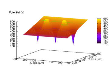
The surface plot of electrostatic potential for a typical MSGC has been presented in Fig.1. Qualitatively, the comparison is found to be acceptable with [7]. In order to carry out quantitative comparison, we have computed electric field on the anode for MSGC-s as presented in Table I of [8] (cases (a) and (b) corresponding to vacuum and dielectric substrates, respectively). As in [8], the computations have been done for two thicknesses of the substrate, namely, 100m and 500m. The electric fields on the anode turn out to be 32.88kV/mm and 35.76kV/mm for a vacuum substrate as the thickness is reduced from 500m to 100m which according to [8] varied from 32.7kV/mm to 36.6kV/mm. Similarly, for a dielectric substrate, the values according to the present computations are 32.8kV/mm and 37.85kV/mm while those in [8] are 32.5kV/mm and 36.9kV/mm. It may be said that the trend of the variation is well represented and the numerical values are reasonably close. The small differences can be attributed to several reasons, the most important being the fact that the present computations are 3D in nature, while those in [8] were 2D.
2.2 Micro Wire Detector
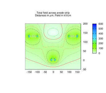
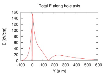
Here we have considered a typical MWD having the dimensions as in [3]. In the following Figs.2(a) and 2(b), we have presented the contours of the electric field on the plane perpendicular to the anode axis and the electric field variation along the hole axis of a typical microwire detector. Once again, the comparison with [3] is found to be satisfactory both qualitatively and quantitatively.
2.3 microMEGAS
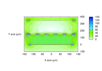
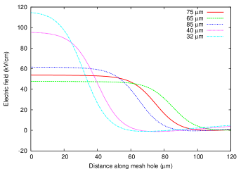
This part of the computation has been carried out in relatively more detail. We have considered several microMEGAS having geometry as discussed in [9] for easy comparison. In Figs.3(a) and 3(b), we have presented the computed electric field surface and contours and the change in the electric field along the center of a mesh hole. These results once again agree with those in [9] reasonably well.
3 Conclusion
Using the neBEM solver, it has been possible for us to estimate the three-dimensional electric field in several micro pattern gas detectors. The accuracy of the obtained results have been confirmed by comparing them with existing 2D BEM and 3D FEM results. Despite having a large length scale variation (1:200) and the use of extremely coarse discretization, the solver has yielded results that are precise and reliable using little computational resource. Since detailed simulation of gas detectors begins with the computation of electrostatic configuration within the device, and depends very critically on the accuracy of the estimated electric field at any arbitrary point within a given device, the neBEM solver is expected to become an important tool in carrying out thorough analysis of gas detectors. This is more true for the new generation detectors since the length scales of these detectors vary widely from component to component.
References
- [1] A. Oed, Nucl. Instrum. and Meth. A 263, p.351 (1988).
- [2] I.Giomataris et al., Nucl. Instrum. and Meth. A, 376 p.29 (1996).
- [3] B.Adeva et al. Nucl. Instrum. and Meth. A, 435 p.402 (1999).
- [4] www.ansoft.com/products/em/max3d
- [5] S. Mukhopadhyay, N. Majumdar, Engg. Analysis Boun. Elem., 30, pp.687-696 (2006).
- [6] N.Majumdar, S.Mukhopadhyay, Nucl. Instr. Meth. Phys. Research, 566, pp.489-494 (2006).
- [7] A.Randewich, M.Sc. thesis submitted to the Department of Physics, University of Manchester (1994).
- [8] S. Schmidt, U. Werthenbach, G. Zech, Nucl. Instrum. and Meth. A, 344 p558 (1994).
- [9] consult.cern.ch/writeup/garfield/examples/micropattern/