![[Uncaptioned image]](/html/physics/0701108/assets/x1.png)
Институт Теоретической и
Экспериментальной Физики
21–06
I.G. Alekseev, V.A. Andreev,
P.E. Budkovsky, E.A. Filimonov,
V.V. Golubev, V.P. Kanavets, M.M. Kats,
L.I. Koroleva, A.I. Kovalev, N.G. Kozlenko,
V.S. Kozlov, A.G. Krivshich, V.V. Kulikov,
B.V. Morozov, V.M. Nesterov, D.V. Novinsky,
V.V. Ryltsov, M.E. Sadler, V.A. Sakharov,
D. Soboyede, A.D. Sulimov, V.V. Sumachev,
D.N. Svirida, V.Yu. Trautman, E. Walker, S. Watson.
![[Uncaptioned image]](/html/physics/0701108/assets/x2.png)
Cost Effective Electronics
for Proportional and
Drift Chambers of
’EPECUR’ Experiment
Москва 2006
УДК 539.1.075 М-16
Cost Effective Electronics for Proportional and Drift Chambers of ’EPECUR’ Experiment. Preprint ITEP 21-06/
I.G. Alekseev, V.A. Andreev, P.E. Budkovsky, E.A. Filimonov, V.V. Golubev, V.P. Kanavets, M.M. Kats, L.I. Koroleva, A.I. Kovalev, N.G. Kozlenko, V.S. Kozlov, A.G. Krivshich, V.V. Kulikov, B.V. Morozov, V.M. Nesterov, D.V. Novinsky, V.V. Ryltsov, M.E. Sadler, V.A. Sakharov, D. Soboyede, A.D. Sulimov, V.V. Sumachev, D.N. Svirida, V.Yu. Trautman, E. Walker, S. Watson. M., 2006-23 p.
’EPECUR’ experiment setup is under construction at the beam line 322 of the ITEP proton synchrotron. The experiment requires several large area drift chambers to provide reasonable acceptance and fine pitch proportional chambers for beam particle tracking with total number of electronic channels of about 7000. New compact and cost effective readout system for these gaseous detectors was designed, prototyped and tested in the latest two years based on the modern technologies in analog and digital electronics, as well as in data transfer protocols. Mass production of the proportional chamber electronics is close to the end, while the boards for the drift chambers are manufactured in the amount to equip one 8-plane module. The paper presents the functional description of the whole DAQ system and its main parts together with some of the test results as an illustration of the excellent performance of the system. The appendix contains specific information which may be useful for the system users or code developers.
НЕДОРОГАЯ ЭЛЕКТРОНИКА ДЛЯ ПРОПОРЦИОНАЛЬНЫХ И ДРЕЙФОВЫХ КАМЕР ЭКСПЕРИМЕНТА "ЭПЕКУР".
И.Г. Алексеев, В.А. Андреев, П.Е. Будковский, В.В. Голубев, В.П. Канавец, М.М. Кац, Л.И. Королева, А.И. Ковалев, Н.Г. Козленко, В.С. Козлов, А.Г. Крившич, В.В. Куликов, Б.В. Морозов, В.М. Нестеров, Д.В. Новинский, В.В. Рыльцов, М.Е. Садлер, В.А. Сахаров, Д. Собоеде, А.Д. Сулимов, В.В. Сумачев, Д.Н. Свирида, В.Ю. Траутман, Е. Уолкер, С. Уатсон, Е.А. Филимонов. М., 2006–23 стр.
Конструирование экспериментальной установки "ЭПЕКУР" идет полным ходом на 322-м пучке протонного синхротрона ИТЭФ. Для проведения эксперимента требуется несколько больших дрейфовых камер, чтобы обеспечить необходимый аксептанс, а также пропорциональные камеры с мелким шагом проволочек для регистрации частиц пучка. Общее число необходимых каналов электроники составляет около 7000. Новая компактная и недорогая система считывания с этих газовых детекторов была разработана и опробована в течение двух последних лет. Система использует новейшие достижения технологий в области аналоговой и цифровой электроники, а также в области протоколов передачи данных. Массовое производство электроники для пропорциональных камер близится к завершению, тогда как платы для дрейфовых камер произведены в количестве, необходимом для оснащения одного 8-плоскостного модуля. В работе представлено функциональное описание системы сбора данных и ее основных частей, а также результаты различных тестов как иллюстрация превосходной работы оборудования. В приложении содержится специфическая информация, которая может быть полезна пользователю системы или разработчику программного обеспечения.
Fig. – 14, refs. – 6 names.
© Институт теоретической и экспериментальной физики, 2006
1. Introduction
’EPECUR’ experiment is primarily aimed at the search of the cryptoexotic narrow nucleon resonance , the non-strange neutral member of the pentaquark antidecuplet [1]. General search for narrow pion-nucleon resonances is also implied. The method is the scan of the invariant mass of system in s-channel in the region (1610–1770) MeV with the explicit detection of and final states, which is essentially a very accurate cross-section measurement of the mentioned processes in very fine steps in energy.
The setup is under construction at the universal beam line 322 of the U-10 synchrotron (ITEP, Moscow). The beam line ideally fits the experiment requirements due to its very good momentum resolution of better than 0.1 % [2] and reasonably high typical intensity of negative pions per accelerator cycle (every 4 seconds). The project is a united effort of ITEP (Moscow), PNPI (St. Petersburg) and ACU (Abilene, USA). The construction started in 2005 from scratch and the beginning of data taking is scheduled on early 2008.
To reach the goal of the experiment two types of tracking detectors are required:
-
a)
small but fast detectors for incident particle tracking and its momentum measurement;
-
b)
large acceptance high accuracy detectors for the tracking of the reaction products.
Both detectors should have as little matter as possible on the way of the particles to minimize multiple scattering and maintain the beam momentum resolution.
Fine pitch proportional chamber is a good solution for a). In addition such detector provides fast trigger capability, allowing to minimize the number of scintillation counters in the beam. Two-coordinate chamber with 1 mm pitch and 200200 mm2 sensitive area has 400 sensitive wires.
Wire drift chambers with hexagonal cell structure [3] and 20 mm cell diameter were selected as the best choice for b). Typical drift chamber module covers 8001200 mm2 area and is a stack of 4 submodules with horizontal, vertical and tilted wire directions. Each submodule has two planes of drift cells, resulting in approximately 530 sensitive wires per module.
The setup at its final stage includes 6 proportional chambers, 5 drift modules of the mentioned size, as well as a twice larger drift module and 4 smaller modules. This gives 2400 proportional and approximately 4300 drift sensitive wires and corresponding number of electronic channels.
Limited funding of the project together with the relatively large number of required electronic channels put out a challenge to built a cost effective data acquisition system for the experiment. To lower the cost the simplest and most compact solution was implemented using only commercially available components. Variety of modern integrated circuits, both analog and digital, together with advanced PCB technology allowed to develop best quality devices meeting the experiment requirements. Interconnection between the parts of the DAQ is based on the wide spread protocols such as USB and Ethernet, allowing application of standard interfacing modules.
During 2005-2006 all parts of the DAQ were designed, manufactured and successfully tested with the prototype detectors. Mass production of proportional chamber electronics and auxiliary hardware is close to the end, while the boards for the drift chambers are in production in the quantity necessary to equip two prototype submodules.
This paper describes the structure of the ’EPECUR’ data acquisition system, as well as the principles of operation of its main components. Selected test results are also presented.
2. ’EPECUR’ DAQ Structure
The data acquisition system is illustrated by Fig. 1 and includes:
-
1.
100-channel proportional boards performing the following functions:
-
•
wire signal amplification and conditioning;
-
•
leading edge pulse discrimination;
-
•
latching of the signals on the arrival of late trigger by means of the digital delay line;
-
•
encoding of the hit wire numbers into the digital data flow;
-
•
transfer of the data through a high speed USB connection;
-
•
forming of the fast trigger output as an OR of all wire hit signals;
-
•
-
2.
24-channel drift boards with similar functionality, but with added time digitization capability and no fast trigger output;
-
3.
locally placed distribution boxes providing power, trigger and USB connections for the boards, as well as the Ethernet interface for the data;
-
4.
DAQ server computer and several workstations for control and monitoring, connected into a local fast Ethernet network.
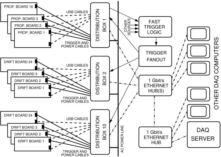
Proportional and drift boards are mounted directly on the chamber frames close to the sensitive wire ends. Each of the boards is connected to a distribution box with a 4-wire USB cable and a 4-pair UTP (Unshielded Twisted Pair) cable carrying power and differential trigger signals.
3. 100-Channel Proportional Chamber Board
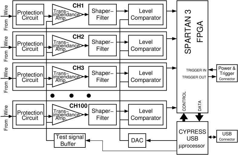
Proportional chamber board (Fig. 2) contains 100 identical analog channels, Xilinx FPGA chip, Cypress USB microprocessor, discriminator level DAC and power conditioning components.
The input of each channel is resistively connected to the ground to provide zero potential to the signal wire. The diode-based low capacitance protection circuit prevents the input from over-voltage in case of spark discharge in the chamber. The fast current sensitive transimpendance amplifier is based on a 1.2 GHz IC chip and provides the signal amplification of 5 mV/A. The RC shaper-filter is designed to cut out the long tail of the charge collection signal and to reduce the high frequency noise component on the amplifier output.
A fast comparator with TTL output is used to form the leading edge discriminator. All channels have common discrimination threshold programmable in 1 mV steps by means of a serial DAC controlled by the microprocessor. The amplitude spread of the signals at the comparator input is in the range of 10 mV to 50 mV. Rather low amplification allows to avoid oscillation problem and makes the amplifier stage cost effective. At the same time a careful choice of the comparator with low offset voltage of several mV is necessary.
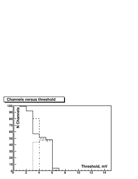
Figure 3 shows the typical results of a board threshold spread test. Due to the bias currents flowing into the comparator inputs, the actual discriminator level is always several mV below the common voltage, applied to the negative comparator inputs. The software can read each channel level state at various DAC settings and thus count the number of trigged channels (with no input signal) as a function of applied threshold voltage. Solid and dashed lines present the number of trigged channels when the threshold voltage is changed in steps of 1 mV from 0 to 15 mV and back, correspondingly. The range of 3 to 5 mV is the region of instability, where many of the channels are very close to their thresholds and start switching synchronously causing positive feedback from the TTL output to the amplifier input. This is the reason why the solid and dashed lines do not coincide. The software can also identify the region where the oscillating switching of the comparator outputs occur; the half number of oscillating channels is presented by the dash-dotted and dotted lines for ascending and descending threshold voltages. As it’s seen from Fig. 3, at threshold voltages above 7 mV all 100 channels are not trigged and ready to accept small signals, while the total threshold spread is 6 mV.
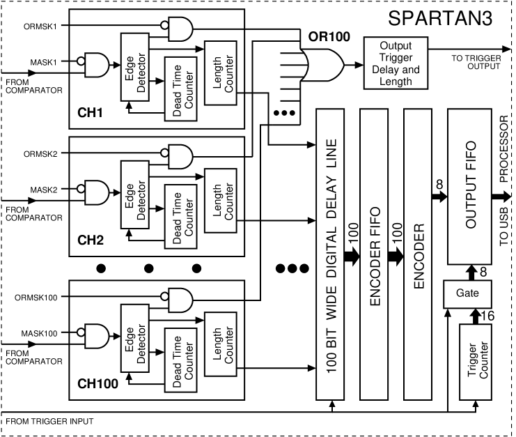
All comparator outputs are tied to the inputs of the Spartan-3 [4] Field Programmable Gate Array (FPGA) chip and all subsequent signal processing is done digitally inside this chip. Figure 4 illustrates the the idea of the configuration implemented in th FPGA.
The leading edge of the signal from the comparator is captured by the ’edge detector’ and starts two counters. The ’length counter’ is intended for producing a signal of several clock periods111The internal clock frequency of the FPGA is 96 MHz, corresponding clock period is about 10 ns. which is then put to the digital delay line. The ’dead time counter’ blocks the further acceptance of signals by the channel for a certain amount of time. This is done to suppress ’ringing’ on the input line caused by the crossing of the comparator threshold by the long and slowly changing charge collection tail. Both counters are separately programmable, but to the same values for all channels (see Table A4). A pulse of one clock period from each channel is used to form the grand OR trigger output. The duration and the delay of the signal on this output are also programmable in one clock period steps. A channel may be completely disabled, or its participation in the grand OR may be forbidden, by setting corresponding MASK or ORMSK bits.
The state of all 100 ’length counter’ outputs is continuously piped through the digital delay line. On the (late) arrival of the actual system trigger a time slice is retrieved from a certain (programmable) depth of the delay line, representing the state of all channels on the time of the event which caused the trigger. This 100-bit wide time slice is stored to the encoder FIFO which provides buffering and ensures dead-timeless operation. The encoder converts the nonzero bit positions in the slice into the sequence of their numbers and directs it to the output FIFO preceded by some control information including the sequential trigger number (see Table A2 for details).
The data is then transferred to the USB microprocessor [5] and buffered there to form an USB packet [6] which can be retrieved on the request from the host computer. Another data line is used by the processor to load and read the programmable registers inside the FPGA. The microprocessor is also responsible for generating the test pulse which is distributed to each analog channel input through a small capacitance.
The microprocessor code and the FPGA configuration firmware is not stored on the board thus eliminating additional cost expenses for the large flash memory chip and saving the board space. Instead, on power up the bootloader hardcoded into the microprocessor retrieves the application code through the USB from the host computer. In turn, this code provides the possibility to configure the FPGA chip with the firmware downloaded by the USB host. In addition such approach gives an extreme flexibility of changing the microprocessor code as well as the FPGA configuration. A very small I2C flash memory is used to keep the board identification and serial numbers which are programmed at the production time.
The summary of USB requests served by the application code is presented in Table A1.
The board dimensions are 275120 mm2 (Fig. 5) and the connection to the chamber is done via the 200 pin two row 90o male header connector (all pins in the second row are the signal ground). Several LED indicators (see Table A6) visualize the board status. Power requirements are listed in the Table 1. The power is supplied to the board through an RJ45 8 pin connector (Table A7) which also provides the trigger connection. Natural convection airflow is enough at room temperature for the board cooling in any position, but forced ventilation is required if the board is placed in a closed volume.
| Supply | Range | Current | Power dissipation |
| +6 V | 5.5–6.5 V | 1.4 A | 8.4 W |
| –6 V | –(5.5–6.5) V | 1.3 A | 7.8 W |
| +4 V | 3.6–4.3 V | 0.4 A | 1.6 W |
| Total power dissipation: | 17.8 W | ||
4. 24-Channel Drift Chamber Board
The structure of the drift chamber board is very similar to that of the proportional one, discussed in the previous section (Fig. 2). The main differences are:
-
•
only 24 analog channels per board;
-
•
faster transimpendance amplifier;
-
•
completely different FPGA configuration with individual channel timing capability;
-
•
additional circuity for temperature and power monitoring;
-
•
smaller board size.
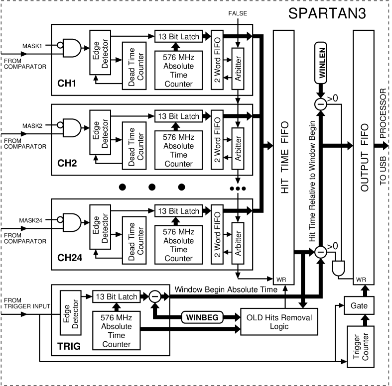
The FPGA configuration for the drift chamber board is presented in Fig 6. The input stage of each channel is similar to that of the proportional design and includes ’edge detector’ and ’dead time counter’. On the detection of the signal the value of the 13-bit absolute time counter is latched and stored to an intermediate ’2 word FIFO’. The equivalent frequency of the counter is 576 MHz, corresponding to 1.74 ns time measurement unit. Each channel has its locally placed absolute time counter to minimize the connection delays on the FPGA crystal. All counters are synchronized on the system initialization and at the beginning of each accelerator cycle period. Nonempty intermediate FIFOs store their content to the main ’hit time FIFO’ arbitrating on the ’channel number priority’ basis. Channel number is stored to the main FIFO together with the absolute time value latched by this channel.

Only those channel hits that fall into a certain window are processed. Two programmable registers (Table A5) are responsible for the definition of this window: WINBEG designates the beginning of the window prior to the arrival of the system trigger, while WINLEN is the window length (see Fig 7).
The absolute time value of the oldest (first in the queue) hit is always present on the main FIFO output. The running value of the ’age threshold’ is continuously calculated by the ’old hits removal logic’ as the absolute time decreased by the WINBEG setting (actually this is ’window begin’ given the trigger arrives at the current moment). The two values are continuously compared and the hit is removed from the FIFO as soon as it becomes older than the ’age threshold’. Thus the oldest hit in the FIFO on the moment of actual trigger arrival will be the first hit falling into the trigger window. The procedure also ensures that the FIFO is never overflown in case no triggers follow the wire signals.
On the detection of the system trigger processing of the channel signals arrived by this time starts. The trigger arrival time is digitized by the separate channel also in terms of the absolute time. The beginning of the actual window is calculated and this value is then subtracted from the consequent hit values from the FIFO to form the hit time values , relative to the window begin. These resulting values are passed to the output FIFO preceded by the sequential trigger number. The procedure stops and the trigger is considered to be served when the main FIFO is empty or a hit value later than the window end is encountered. The hits left in the FIFO will either become ’old’ and be removed or picked up by the next trigger window.
Processing of each hit in the window takes one CLK2 period222CLK2 frequency is 48 MHz, corresponding period is about 20 ns, so the trigger service time is proportional to the number of hits in the window. During this service time other triggers appearing on the input do not start the hit selection procedure, but increment the trigger counter. During the data taking, if even some triggers are lost, probably differently in different boards, the trigger number preceding the data of a certain event will always be the same in all boards.
In case of frequent triggers, the trigger windows of the consequent triggers may overlap. In this case the earlier trigger will sweep the hits from the main FIFO, which might also correspond to the later one. This possibility should be taken into account in the data processing.
The further data transferring in the drift chamber board is essentially the same as in the proportional one, except that the structure of the data flow is different reflecting the timing capability (Table A3).
The board dimensions are 30050 mm2 (Fig. 5), connection to the chamber is done via the two 24 pin two row 90o male header connectors (as in the proportional design, every second pin is signal ground). LED indicators are similar to those of the proportional board (Table A6). Power requirements are listed in the Table 2. Power and trigger connection is the same as in the proportional design (Table A7), so that the same cables can be used for both types of the boards. Power dissipation is more than 3 times less than that of the proportional board, yet forced airflow should be used for cooling if many of the boards are placed in a closed volume.
| Supply | Range | Current | Power dissipation |
| +6 V | 5.5–6.5 V | 0.33 A | 2.0 W |
| –6 V | –(5.5–6.5) V | 0.31 A | 1.9 W |
| +4 V | 3.6–4.3 V | 0.4 A | 1.6 W |
| Total power dissipation: | 5.5 W | ||
5. Distribution Box
In the framework of ’EPECUR’ DAQ system the data is transferred from the chamber boards by means of universal serial bus (USB) [6]. This approach has many obvious advantages, based on the fact that USB is well developed and widely spread:
-
•
high transfer speed 480 Mbit/s;
-
•
thin 4 wire connection cable;
-
•
up to 127 ’devices’ on one branch;
-
•
’device’ side controller chips are readily available and relatively cheap;
-
•
software development tools are well developed for both ’host’ and ’device’ sides;
-
•
many standard items are commercially available (i.e. cables, connectors, hubs etc.).
The main disadvantage of USB is the 5 m limit on a single connection cable length, while the experiment requires transferring of the data for distances up to 100 m.
To solve this problem the distribution boxes were developed, which are placed locally near the chambers and serve as an intellectual interface collecting data from the boards through the USB and sending them to the server computer by means of fast Ethernet.
At the same time power and trigger signals need to be delivered to the boards. Placing of the power supplies and trigger distribution logic into the same box with the data interface allows to make the system most compact.
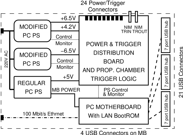
To achieve minimum cost most of the components used in the distribution box are just commercially available blocks. The distribution box contents is illustrated in Fig. 8 and includes:
-
•
standard Pentium based motherboard with USB, Ethernet LAN, parallel and serial controllers on it and enabled ’LAN boot’ feature;
-
•
regular PC power supply (PS) providing power to the motherboard and control circuits on the distribution board;
-
•
two equally modified standard 300 W PC power supplies, capable of up to 25 A current on main low voltage supply lines;
-
•
3 USB hubs, 7 port each, allowing up to 25 USB connections together with 4 USB ports on the motherboard;
-
•
specially designed distribution board, performing the following functions:
-
–
power distribution for up to 24 boards through RJ45 connectors;
-
–
additional power filtering and reverse voltage protection;
-
–
conversion of the NIM system trigger signal to LVDS and its multiplication for individual boards;
-
–
reception of the LVDS grand OR triggers from the proportional chambers, performing majority coincidence function on them and conversion of the resulting signal to NIM for further use by the fast system trigger logic;
-
–
conditioning of the PS status signals and making them available for the motherboard through the serial port modem lines;
-
–
providing remote board power control (on/off) using another serial port line;
-
–
programming of the fast Xilinx CPLD [7], which performs majority coincidence, by means of the motherboard parallel port;
-
–
visible LED indication of all power lines and trigger signals.
-
–
The distribution box is capable of serving up to 24 drift chamber boards, but only up to 16 proportional chamber boards due to the current limit of the power supplies. The box is connected to the outer world by means of only 4 cables:
-
•
AC line cable;
-
•
fast Ethernet cable;
-
•
two coaxial cables, transferring NIM triggers to and from the box.
The box dimensions are mm3 (WHD). The power consumption from the AC line strongly depends on the number of boards connected to the box but does not exceed 400 W. Three power supply fans provide sufficient cooling airflow inside the whole box.
6. Selected Test Results
Both types of boards and the whole DAQ system underwent a lot of various tests both on laboratory tabletop and in real beam conditions. The detailed description of the test procedures is beyond the scope of this paper, yet some of the test results would give a good illustration of the system performance.
The proportional boards were tested with 1 mm pitch 200200 mm2 proportional chambers both with a radioactive -source and with proton beams of the ITEP synchrotron and of the PNPI cyclotron. Two gas mixtures were tried: Ar(67%)CO2(33%) and Ar(75%)C4H10(24.7%)CF3Br(0.3%), so called ’magic mixture’. Both variants showed excellent performance in various beam conditions, except that the first gas mixture is efficient at potential plane voltages about 300 V higher than that for the ’magic mixture’.
The figures below illustrate the typical performance of the proportional system under the following conditions:
-
•
collimated -source;
-
•
chamber load /s;
-
•
trigger rate s-1;
-
•
’magic’ gas.
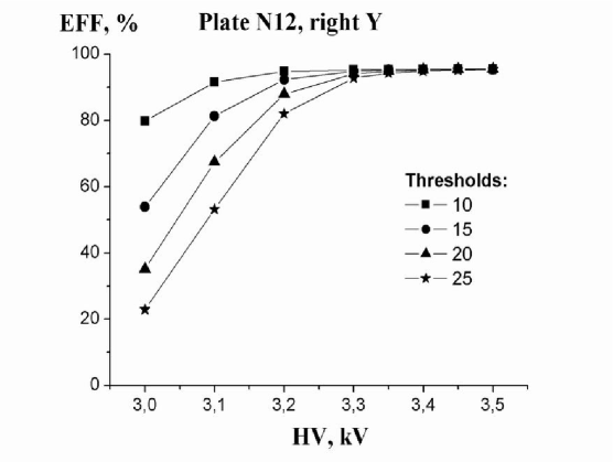
Figure 9 shows the efficiency of the chamber as a function of the applied high voltage at various discriminator threshold settings. The maximum value is lower than 100% due to the relative geometry of the chamber and the trigger scintillation counter. Yet a reliable plato of 100–200 V can be observed for all threshold values.
 a)
b)
a)
b)
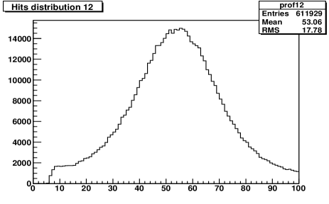
The distribution of the number of hits detected in the chamber for a given trigger is shown in Fig. 10a. Some events in zero bin account for the geometrical inefficiency. Nearly 60% of particles produce exactly one hit in the chamber. About 30% of the events give two hits, which is natural if charge division between adjacent wires for inclined tracks is taken into account. Figure 10b is obtained at the same conditions and represents the profile distribution of the source beam. Only one 100-channel board is active and the source is centered in the half-plane, corresponding to this board. The leftmost 6 wires are insensitive by the chamber design.
1 mm pitch proportional chambers are considered to be difficult to work with, compared to commonly used 2 mm ones. Yet the designed system shows excellent performance even in this case.
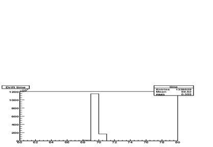
The drift chamber boards are more complicated in functionality. Their time measurement capability was paid special attention to during the testing. One of the tests is briefly described below. A random pulse derived from a PMT noise was applied to one or several channel inputs, while the trigger was made of this signal by delaying it on a fixed cable line for a few hundred nanoseconds. The drift board essentially measures the time between the signal and the trigger, so one would expect constant measured time for this test. The result of this test is presented in Fig. 11. The signal and trigger arrival times are digitized independently, so it’s quite natural that the measured difference is distributed between two adjacent bins. Monotonicity and linearity of the conversion was also checked by changing the cable delay in 0.5 ns steps and recording the peak positions.
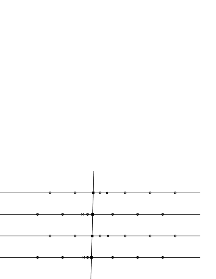
Most of the beam tests of the drift board were performed with a small prototype drift chamber with hexagonal structure, which is designed in a form of a barrel. Cell diameter is 20 mm and 24 cells are arranged into 4 sensitive planes, two of them shifted half cell diameter. Such design allows to perform best track reconstruction like it is shown in Fig. 12.
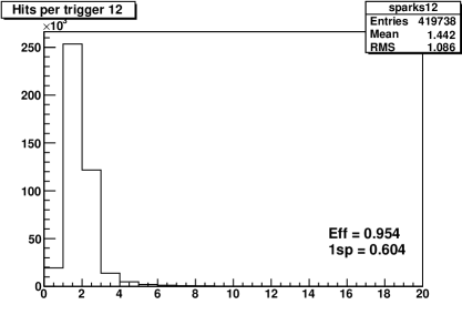
Looking at Fig. 13a which presents the number of hits per trigger in the barrel exposed to a focused beam perpendicular to the sensitive planes, one can make conclusions on the chamber efficiency. About 67% of events give exactly one hit in each plane, resulting in strong maximum at 4 hits per trigger. Small fraction of 5- and 6-hit events (about 20%) represents the cases, when in one or two planes charge division between adjacent cells occurred. Number of 3-hit events is a real measure of a single plane inefficiency and the resulting number is 4.7%. Noticeable amount of zero-hit events can be accounted by the trigger quality as well as by the effect of the trigger window overlapping, which becomes not negligible at trigger rates as high as s-1 and 1 s window length. It’s worth mentioning that the efficiency picture remains essentially the same in wide ranges of applied high voltages and discriminator threshold settings.
 a)
b)
a)
b)
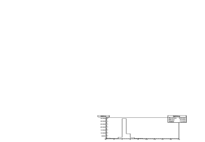
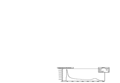
Figure 13b presents the distribution of the drift time in the cells with defocused perpendicular beam (nearly flat beam density over the cell size). Due to the dependence of the drift field the distribution density significantly increases for small drift times, while the bump on the right side of the figure corresponds to the very long drift times of the charges, produced in the area of zero field close to the cell boundary. This distribution can be used for building the drift function giving the hit spatial coordinate by the measured drift time.
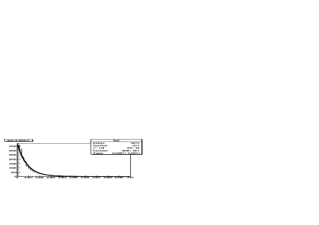
The final goal of the tests of the drift chamber in conjunction with the designed electronic boards was to understand the spatial accuracy of the whole system. The capability of the barrel for the straight track reconstruction allows to perform the accuracy analysis. For 4-hit tracks the distribution of sums of deviations squared should be a distribution with 2 degrees of freedom which has a form of exponential function. If properly normalized, the exponent value gives the average hit deviation from the best straight track, i.e. the coordinate accuracy of a single drift cell. Such a distribution together with its exponential fit is presented in Fig. 14. The cell radius is taken for the coordinate measurement unit, so that the resulting exponent value should be multiplied by 8.5 mm to get the cell accuracy (180 m). The accuracy has only very weak dependence on the high voltage on the potential wires (i.e. the gaseous amplification) and on the discriminator threshold setting, even in cases when the cell efficiency significantly drops. This result is not completely understood yet, since all the empirical considerations state that the accuracy should decrease when the signal amplitude becomes smaller.
7. Conclusions
The data acquisition system for the proportional and drift chambers of the ’EPECUR’ experiment was designed, tested and produced in ITEP in less than 2 years. Taking advantages of modern electronic technologies a really cost effective and compact DAQ system was build and showed excellent performance features. Tests with chamber prototypes showed good efficiency even with 1 mm proportional chmabers and resulted in 180 m spatial accuracy in hexagonal drift cells.
The system is a keystone of the ’EPECUR’ experiment and the ’EPECUR’ team hopes that the fast progress in the setup construction in spite of all difficulties will lead them soon to excellent physics results.
8. Acknowledgments
The authors express heartiest thanks to Dr. Nikolay Bondar’, the member of PNPI HEPD Radio Electronic Department, for useful discussions on the chamber electronics.
’EPECUR’ project is carried out under the financial support of the Russian Federal Agency on Atomic Energy. The work is also partially supported by the Russian Fund for Basic Research grant 05-02-17005a.
Appendix. Proportional and Drift Boards Programming Reference
| Endpoint 0x0/0x80: Standard control endpoint1 with added specific requests | ||||||
| RqType | Request | Value | Index | Length | Data | Description |
| 0x40 | 0x20 | X | X | 0 | – | Generate PROG pulse to FPGA to start configuration |
| 0x40 | 0x21 | X | X | len | data[len] | Load bitstream of ’len’ bytes to FPGA |
| 0x40 | 0x22 | data | 0 | 0 | – | Write low byte of ’data’ to threshold DAC |
| 0x40 | 0x22 | X | 1 | 0 | – | Enable dataflow from FPGA to USB Endpoint 0x82 |
| 0x40 | 0x22 | X | 2 | 0 | – | Disable dataflow from FPGA to USB Endpoint 0x82 |
| 0x40 | 0x22 | X | 3 | 0 | – | Generate a test pulse on the internal line |
| 0x40 | 0x22 | X | 4 | 0 | – | Generate a pulse on the test output |
| 0x40 | 0x22 | X | 5 | 0 | – | Send ’Packet End’ to USB Endpoint 0x82 |
| 0x40 | 0x23 | X | 0 | 16 | data[16] | Write 16 bytes of ’data’ to I2C EEPROM |
| 0x40 | 0x24 | data | addr | 0 | – | Write low byte of ’data’ to FPGA register #’addr’ |
| 0xC0 | 0x20 0x21 | X | X | 1 | done | Read FPGA DONE condition |
| 0xC0 | 0x22 | X | X | 4 | data[4] | Read status (data[0]), DAC setting (data[1]) and board temperature2 (data[2]&data[3], 10 bit left justified) |
| 0xC0 | 0x23 | X | 0 | 16 | data[16] | Read 16 bytes from I2C EEPROM |
| 0xC0 | 0x24 | X | addr | 1 | data | Read byte from FPGA register #’addr’ |
| Endpoint 0x82: Bulk endpoint (only IN direction) | ||||||
| Main data endpoint, for the dataflow structure see Table A2 | ||||||
Notes:
| Byte# | Bit7 | Bit6 | Bits[5:0] | Description |
| 0 | 1 | 0 | TRNUM1[12:7] | Trigger signature and upper part of trigger number |
| 1 | 0 | TRNUM1[6:0] | Lower part of trigger number | |
| 2 | 0 | CHNUM1[6:0] | Number of first channel hit in this trigger | |
| … | 0 | … | Numbers of other channels hit in this trigger | |
| n+2 | 0 | CHNUMn[6:0] | Number of last channel hit in this trigger | |
| n+3 | 1 | 0 | TRNUM2[12:7] | Trigger signature and upper part of next trigger number |
| n+4 | 0 | TRNUM2[6:0] | Lower part of next trigger number | |
| n+5 | 0 | CHNUM[6:0] | Number of first channel hit in this trigger | |
| … | 0 | … | Numbers of other channels hit in this trigger | |
| … | … | … | Other trigger blocks in this cycle | |
| m-1 | 1 | 1 | CYNUM[12:7] | Cycle signature and upper part of cycle number |
| m | 0 | CYNUM[6:0] | Lower part of cycle number | |
| … | … | … | Next cycle data | |
| Byte# | Bit7 | Bit6 | Bits[5:0] | Description |
| 0 | 1 | 1 | 111111b | Trigger signature |
| 1 | 0 | 0 | TRNUM1[5:0] | Lower part of trigger number |
| 2 | 0 | 0 | TRNUM1[11:6] | Upper part of trigger number |
| 3 | 0 | 1 | 0 & CHNUM1[4:0] | First hit channel number |
| 4 | 0 | 0 | TIME1[5:0] | Lower part of this channel time |
| 5 | 0 | 0 | TIME1[11:6] | Upper part of this channel time |
| … | 0 | … | Numbers and times of other channels hit in this trigger | |
| 3n | 0 | 1 | 0 & CHNUMn[4:0] | Last hit channel number |
| 3n+1 | 0 | 0 | TIMEn[5:0] | Lower part of this channel time |
| 3n+2 | 0 | 0 | TIMEn[11:6] | Upper part of this channel time |
| 3n+3 | 1 | 1 | 111111b | Next trigger signature |
| 3n+4 | 0 | 0 | TRNUM2[5:0] | Lower part of next trigger number |
| 3n+5 | 0 | 0 | TRNUM2[11:6] | Upper part of next trigger number |
| … | 0 | … | Numbers and times of channels hit in this trigger | |
| … | … | … | Other trigger blocks in this cycle | |
| 3k | 1 | 0 | 111111b | Cycle signature |
| 3k+1 | 0 | 0 | CYNUM[5:0] | Lower part of cycle number |
| 3k+2 | 0 | 0 | CYNUM[11:6] | Upper part of cycle number |
| … | … | … | Next cycle data | |
| Address | Name | Fields and description |
| 0 RW | CSR0 | CSR0[7:0]=DLY[7:0] – The delay of the 100-bit digital delay line, CLK1 periods |
| 1 RW | CSR1 | CSR1[0]=DLY[8] CSR1[3:1]=DTIM[2:0] – Channel dead time: CLK periods CSR1[5:4]=OLEN[1:0] – Channel output duration for putting to the digital delay line, CLK periods CSR1[6] – Trigger source select: 0 – External from RJ45 connector; 1 – Internal, grand OR of all channels OR generated by SFT_TR CSR1[7] – Enable data transfer to the processor |
| 2 RW | CSR2 | CSR2[7:0]=TRGDLY[7:0] – Additional delay of the grand OR trigger to the output, CLK periods; if TRGDLY=0, output is forbidden |
| 3 RW | CSR3 | CSR3[3:0]=TRGLEN[3:0] – Length of the grand OR trigger on the output, TRGLEN+1 CLK periods CSR3[6:4] – Reserved CSR3[7] – Enable accelerator cycle emulator (period 2.8 s, inhibit 0.35 s) |
| 4 W | RST | Various resets, selected by the written mask: RST[0] – Reset all FIFOs RST[1] – Trigger counter clear RST[2] – Cycle counter clear RST[7:3] – Reserved |
| 5 W | SFT_TR | Writing of any number causes a trigger if enabled with CSR1[6] |
| 4–5 R | CYNUM | CYNUM[15:0] – Last cycle number |
| 6–18 RW | ORMSK | ORMSK[99:0]2 – Bit mask inhibiting individual channel participation in the grand OR trigger output; |
| 19–31 RW | MASK | MASK[99:0]2 – Bit mask completely inhibiting individual channels |
| 32–44 R | INLVL | INLVL[99:0]3 – Bit representation of logic levels on individual channel inputs |
| 45 R | 0 | Always read 0 |
| 46–47 R | TRNUM | TRNUM[15:0] – Last trigger number |
Notes:
-
1.
CLK frequency is 96 MHz.
-
2.
4 most significant bits are RW, but have no effect.
-
3.
4 most significant bits always read 0
| Address | Name | Fields and description |
|---|---|---|
| 0 RW | CSR0 | CSR0[7:0]=WINBEG[7:0] – Trigger window start prior to the trigger, lower part, CLK11 periods |
| 1 RW | CSR1 | CSR1[2:0]=WINBEG[10:8] – Trigger window start, upper part CSR1[7:3]=WINLEN[4:0] – Trigger window length2, lower part, CLK11 periods |
| 2 RW | CSR2 | CSR2[4:0]=WINLEN[9:5] – Trigger window length, upper part CSR2[7:5]=DTIM[2:0] – Channel dead time: CLK23 periods |
| 3 RW | CSR3 | CSR3[0] – Trigger source select: 0 – External from RJ45 connector; 1 – Internal, from the processor CSR3[2:1] – Power monitor select: 0 - positive analog supply 1 - comparator digital supply 2 - FPGA core supply 3 - negative analog supply CSR3[6:3] – Reserved CSR3[7] – Enable data transfer to the processor |
| 4 W | RST | Various resets, selected by the written mask: RST[0] – Reset all FIFOs, emulate cycle end RST[1] – Trigger counter clear RST[2] – Cycle counter clear RST[7:3] – Reserved |
| 5–7 RW | MASK | MASK[23:0] – Bit mask completely inhibiting individual channels |
| 8–10 R | INLVL | INLVL[23:0] – Bit representation of logic levels on individual channel inputs |
| 11 R | PWMON | Power monitor reading, selected by CSR3[2:1] |
| 12–13 R | CYNUM | CYNUM[15:0] – Last cycle number |
| 14–15 R | TRNUM | TRNUM[15:0] – Last trigger number |
Notes:
-
1.
CLK1 frequency is 144 MHz.
-
2.
The trigger window ends not later than the actual trigger comes, so that values greater than WINBEG are useless.
-
3.
CLK2 frequency is 48 MHz.
| Prop. | Drift | Color | Description |
|---|---|---|---|
| D53 | D2 | Green | +5V Analog power |
| D54 | D3 | Green | -5V Analog power |
| D60 | D4 | Green | +3.3V Digital power |
| D56 | D30 | Yellow | Heartbeating: regularly flashes when the application code is running in the processor |
| D57 | D31 | Yellow | Flashes on USB control endpoint requests |
| D58 | D32 | Yellow | Flashes on a trigger from any source accepted by the board, lights between accelerator cycles |
| D59 | D33 | Yellow | Flashes on data transfers from FPGA to the processor |
| D61 | D1 | Red | Lights when the FPGA is not configured |
| Pin# | Description |
|---|---|
| 1 | LVDS trigger input |
| 2 | LVDS trigger input complimentary |
| 3 | Power +6 V |
| 4 | Power +4 V |
| 5 | Power V |
| 6 | Power return ground |
| 7 | LVDS trigger output1 |
| 8 | LVDS trigger output complimentary1 |
Notes:
-
1.
In drift chamber boards the LVDS trigger outputs are always driven passive.
-
2.
A standard UTP Ethernet cable can be used for the power and trigger connection.
References
- [1] I.G. Alekseev et al. Search for the Cryptoexotic Member of the Baryon Antidecuplet 1/2+ in the Reactions and . Preprint ITEP 2-05; hep-ex/0509032.
- [2] L.Z. Barabash et al. Methods and Results of Tuning the Universal Secondary Particle Channel of the Reconstructed ITEP Proton Synchrotron. Preprint ITEP 115-1975.
- [3] G.D. Alkhazov et al. Forward Spectrometer for Study of Low-lying Baryon Resonances. SPES4- Experiment at Saturne-II Accelerator (Saclay). Preprint PNPI 2352-EP-9-2000.
- [4] Spartan-3 Complete Data Sheet. http://direct.xilinx.com/bvdocs/ publications/ds099.pdf.
- [5] EZ-USB FX2LPTM USB Microcontroller. http://download.cypress.com/ published-content/publish/design_resources/datasheets/con- tents/cy7c68013a_8.pdf.
-
[6]
Universal Serial Bus Revision 2.0 Specification.
http://www.usb.org/developers/docs/usb_20_05122006.zip. -
[7]
XC2C32A CoolRunner-II CPLD.
http://direct.xilinx.com/bvdocs/publications/ds310.pdf.
Подписано к печати 14.12.06. Формат 60х90 1/16 Усл.-печ. л. 1,5 Уч.-изд. л. 1,1 Тираж 120 экз. Заказ 21 Индекс 3649 Отпечатано в ИТЭФ, 117218, Москва, ул. Б. Черемушкинская, д. 25
Индекс 3649
Препринт 21–06, ИТЭФ, 2006