All-optical atom surface traps implemented with one-dimensional planar diffractive microstructures
Abstract
We characterize the loading, containment and optical properties of all-optical atom traps implemented by diffractive focusing with one-dimensional (1D) microstructures milled on gold films. These on-chip Fresnel lenses with focal lengths of the order of a few hundred microns produce optical-gradient-dipole traps. Cold atoms are loaded from a mirror magneto-optical trap (MMOT) centered a few hundred microns above the gold mirror surface. Details of loading optimization are reported and perspectives for future development of these structures are discussed.
pacs:
32.80.Pj,81.16.Ta,39.25.+kI Introduction
Manipulation and control of matter at the micro- nano- and atomic level has become increasingly important for the investigation of cold quantum gases HHH01 , atom interferometry WAB05 , quantum information processing WHS06 and precision positioning of atoms on or under surfaces MHP04 ; LRH05 . For the most part magnetic forces have been used in order to take advantage of favorable scaling laws and on-chip integration technologies as component size reduces to the micron scale WL95 ; RHH99 ; CCF00 . The implementation of optical forces has proceeded more slowly because the subwavelength electro-magnetic field localisation required to achieve comparable scaling-law advantages has been more difficult to realize. Earlier work has emphasized remote, table-top preparation of optical trap arrays with subsequent projection into the closed vacuum system containing the cold atoms DVM02 or the use of “optical tweezers” either for long-range transport of cold-atom condensates GCL02 or for the sorting of individual atoms in 1D strings MAD06 . Recent developments in integrated- and nano-photonics nano , however have renewed interest in all-optical approaches to atom and molecule manipulation using on-chip planar architectures ETP05 ; O06 . Optical forces are of interest because of their wide applicability to atoms, molecules and clusters. They rely on electrical polarization, independent of net magnetic dipole moment, while most molecules are singlets with no net magnetic dipole in the electronic ground state. Here we report a study using planar diffractive focusing to load an elongated optical dipole trap with cold atoms from a 3-D mirror magneto-optical trap RHH99 oriented m above a gold mirror surface.
II Overall Experimental setup
Figure 1 shows a schematic of the overall setup.
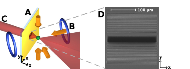
The MMOT, cooling and repumping near the Cs [=4] Cs [=5] and the Cs [=3] Cs [=3] transitions respectively, produces a cloud of cold cesium atoms several hundred microns from the gold mirror surface. The MMOT is loaded from background Cs vapor and captures atoms with a density of cm-3 at a temperature of K. The surface itself is formed from a gold layer 400 nm thick evaporated onto a 25 mm square, 1 mm thick fused silica substrate. Two laser beams reflect in the horizontal plane while two counterpropagating beams along the vertical axis plus the external magnetic field gradient complete the standard six-beam MOT configuration. A focused ion beam (FIB) is used to mill at the mirror center a pattern of horizontal slits so as to produce a Fresnel diffraction lens with a 1-D focus. When illuminated from behind the mirror with an intense laser beam tuned far to the red of the Cs D2 line, the structure forms a Fresnel far-off resonance dipole trap (FFORT). This FFORT is loaded with cold atoms from the MMOT. We have studied cold Cs atom trapping using diffractive structures with focal lengths of 500 m and 200 m.
II.1 Fresnel Lens Characterization
In order to verify the planar Fresnel lens designs we developed a separate test setup that directly measures the focal properties of these devices. Figure 2 shows the arrangement.
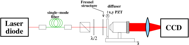
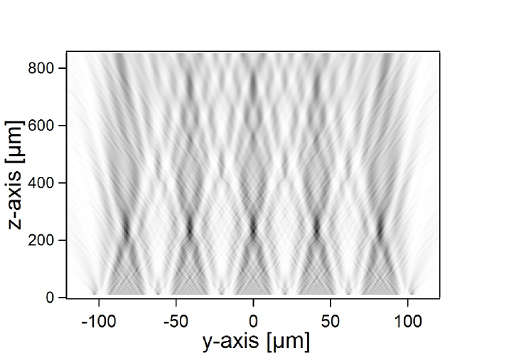
A laser beam issuing from a stabilized laser diode coupled to a single-mode fiber is linearly polarized and impinges on the FIB-milled Fresnel structure from the back (substrate side). A diffuser plate placed on the output side maps the spatial intensity of the diffracted light in planes parallel to the structure plane. A piezoelectric element dithers the diffuser plate in the plane to eliminate the effects of speckle, and a microscope objective images the diffuser intensity pattern onto a CCD camera. The distance between the diffuser-plate-imaging-objective combination and the Fresnel structure is systematically increased along . At each distance an image of the pattern is recorded on the CCD camera and integrated along , the long axis of the Fresnel slits, thereby generating a series of profiles of the intensity distribution along as a function of . The resulting measured intensity map in the plane is then compared with numerical simulations to verify design accuracy. Figures 4 and 4 show the measured profile and the numerical simulation respectively for the 500 m focal length Fresnel motif.

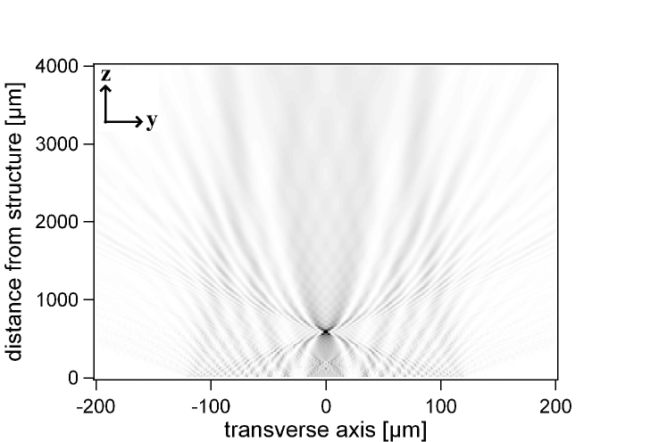
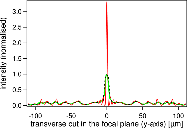
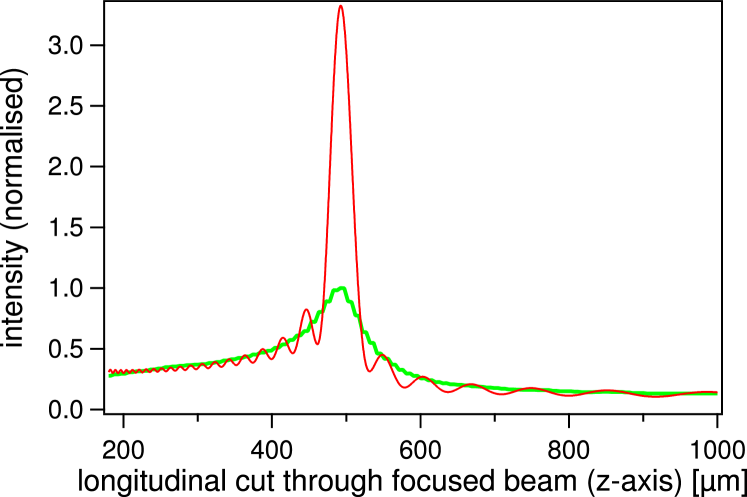
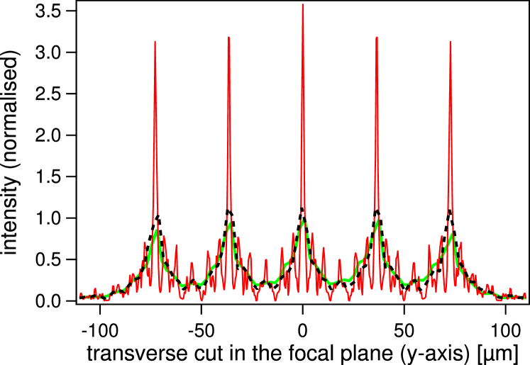
The intensity profiles in the transverse focal plane and along the longitudinal axis are plotted in Figs. 6 and 6. These plots show that the simulated transverse focus profile (red curve) is significantly sharper than the measured CCD image (green curve). The black-dashed curve shows the simulated focal profile averaged over the effective spatial resolution of 2.4 m ( image magnification; CCD pixel element 24 m square). Overall dimensions of the simulated focal spot along the directions are 192 m, 2 m, 35 m, respectively. The excellent agreement between the measured profile and the spatially averaged calculated profile indicates that the red-curve simulation well represents the actual focus characteristic of the Fresnel lens. These results support and encourage the use of numerical simulations to explore more elaborate lens designs.
II.2 Atom Trap Imaging System
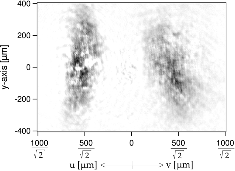
The atoms trapped in the MMOT and in the FFORT are imaged by an absorption profile of a probe laser beam tuned near the transition. Figure 7 shows a schematic of the absorption imaging system which registers a double image: one from atom absorption followed by mirror reflection, the other from mirror reflection followed by atom absorption. We therefore obtain two projections from orthogonal directions and thus a 3D view of the atom distribution.
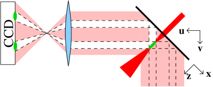
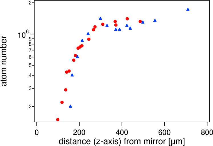
Figure 9 shows a typical image of the distribution of cold atoms trapped in the MMOT when the trap center is located m away from the mirror surface. The optical thickness of trapped atoms in the MMOT would be sufficient to attenuate the probe laser beam almost to extinction if tuned to the absorption resonance peak. Therefore, for the MMOT images, the probe is tuned off-resonance by about four natural atomic line widths in order to maintain linearity between absorption probability and atom number. For atoms trapped in the FFORT, the imaging laser is resonant with the transition. The distance from the MMOT to the mirror plane can be varied either by mechanically moving the mirror closer to the atoms with a vernier screw adjustment or by adding a bias magnetic field that translates the cloud center. Figure 9 shows that the minimum distance before atom loss from the trap becomes significant is m. We believe that the onset of this loss occurs because the vertical beams of the MMOT are partially occulted by the mirror. At the center of the mirror the resulting sharp edge diffraction produces a shadow about 100 m wide that begins to perturb the MMOT loading rate at a comparable distance from the mirror surface.
Note that since the Fresnel lens is engraved on the mirror, all beams reflecting on the surface are diffracted by the structure. This includes the imaging beam, whose diffracted part is not collected by the imaging lens. There is therefore a region where we lose all information about the number of atoms. From geometrical considerations, the size of this blind region is half the width of the structure in the direction, so typically 100 m. In the next generation of structures, this size will be reduced to obtain a 75 m x 200 m footprint. Absorption is thus decreased by a factor of 3 but this reduction permits imaging atoms down to 35-40 m above the surface.
III FFORT atom loading from MMOT
III.1 Trapped atom number
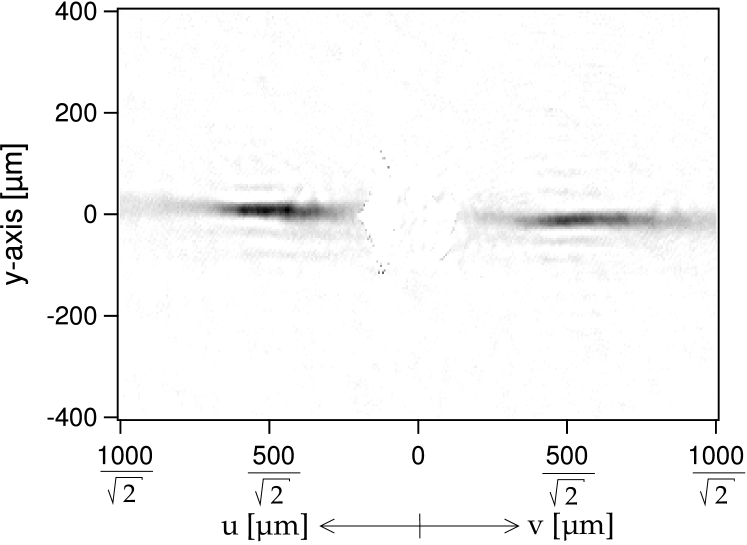
We have carried out a series of measurements to optimize FFORT loading from the MMOT. Figure 11 shows an absorption image of the atoms trapped in the FFORT with 500 m focal length. We have also investigated 200 m focal length structures; but, in addition to atom loss from mirror proximity (Fig. 9) technical limitations associated with imaging discussed in section II.2, restrict systematic studies reported here to 500 m focal-length devices.
We first measured the trapped atom number as a function of FFORT laser power. The results are shown in Fig. 11 and, above a threshold of 20 mW, indicate a linearly increasing number of atoms. As the trapping laser power grows, the effective volume of the FFORT grows as well — first in the central focal region, then in the small secondary maxima adjacent to the main peak (see Figs. 6, 6). For these measurements the dipole-gradient trap laser detuning was fixed at nm to the red of the Cs resonance line.
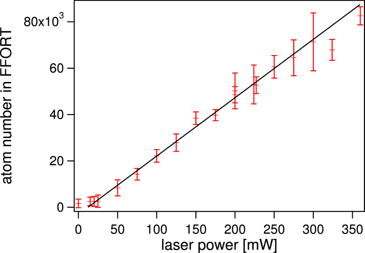
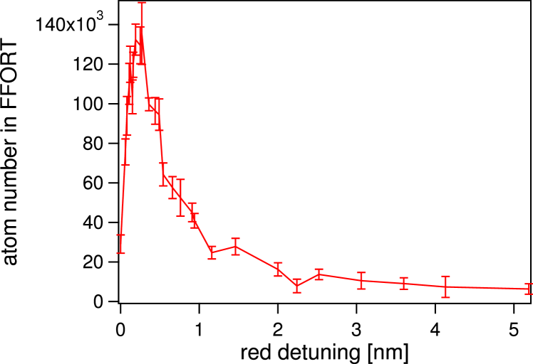
Next Fig. 13 plots the atom number in the FFORT as a function of red detuning. We found that a detuning of nm produced the optimum atom number. The rapid fall-off at smaller detunings is due to absorptive heating while at larger detunings it is primarily due to the inverse relation between trap depth and detuning. The data shown in Figs. 11, 13 were recorded 30 ms after extinguishing the MMOT so as to purge untrapped atoms from the imaging field of view.
III.2 Loading efficiency
We also determined loading efficiency, defined as the ratio of trapped atoms to the initial atom number in the MMOT. The relatively poor spatial overlap between the MMOT and the FFORT (compare Figs. 9, 11), results in a rather low loading efficiency of only a few per cent.
In order to evaluate the number of trapped atoms initially in the volume of the diffraction pattern of the lens, we carried out an optical pumping experiment through the structure. With the dipole trap laser off, we first pump all MMOT atoms (Cs [=4]) to the =3 state with a 200 s pulse resonant on the transition. Then, we illuminate the structure from behind with a resonant 200 s pulse, which pumps the atoms back to the =4 state. As this laser goes through the lens, only the atoms in the diffraction pattern are affected. We then take a usual absorption image on the transition. Atoms outside the diffraction pattern are still in the state, and thus transparent to this probe. Comparing the number of atoms in the central peak of this distribution to the number of atom in the FFORT, we can conclude that the capture efficiency of the dipole trap approaches unity.
III.3 Temperature after release
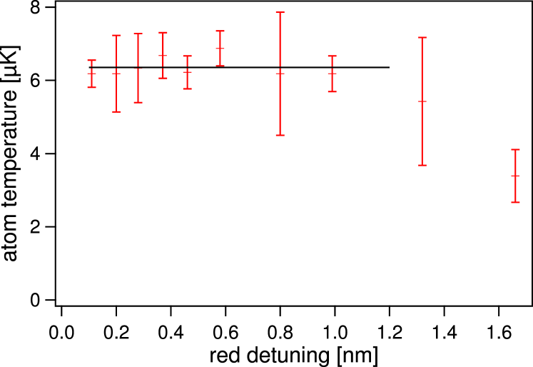
Finally we also measured the atom temperature in the confining direction within the trap by monitoring the atom cloud ballistic expansion after trap release GW00 . The results, as a function of trap detuning are shown in Fig. 13. The FFORT-trapped atoms are found to be significantly colder than the atoms in the MMOT (K vs. K). The origin of this extra cooling effect has not yet been thoroughly investigated. However from numerical simulation we estimate the trapping frequency along the confining axis to be about 13 kHz. Since a mechanical shutter extinguishes the FFORT in about 1 ms, we speculate that part of the cooling effect comes from adiabatic expansion just prior to ballistic release. Note also that the temperature starts to decline with detuning beyond 1 nm, where decreasing trap depth might lead to some evaporative cooling effect.
IV Perspectives
Several different directions for development of these planar, all-optical atom trapping structures remain to be exploited. As the work presented here shows, the most promising involve not only miniaturisation but integration of structure functionality directly onto the chip. First, we are investigating 1D trap arrays as shown in Figs. 15 and 15 and 2D arrays as well. We are also developing variable-focal-length lenses useful for capturing atoms far from the mirror and guiding them into very small volumes close to the surface. Second, we are exploring the integration of the optical structures with on-chip microelectronic circuitry and micromechanical (MEMS) devices for each array element. Dynamic addressing of the trapped cold atoms either electrically with integrated current-carrying wires or optically with laser spots provide typical examples. Finally, miniaturization can be greatly improved by reducing the size of FIB-milled Fresnel elements while maintaining adequate trapping efficiency. Further reduction to about a 10 m footprint should be possible by taking advantage of subwavelength surface wave phenomena LDD02 ; GAV06 . Development of planar arrays together with atom transport and dynamic array-element addressing, opens the way to applications in quantum gate implementation and precision atom doping of surfaces.
Acknowledgements.
Support from the Ministère délégué à l’Enseignement supérieur et à la Recherche under the programme ACI-“Nanosciences-Nanotechnologies,” the Région Midi-Pyrénées [SFC/CR 02/22], and FASTNet [HPRN-CT-2002-00304] EU Research Training Network, is gratefully acknowledged. Technical assistance of H. Lezec and the fabrication facilities of the Caltech Kavli Nanoscience Institute are also gratefully acknowledged.References
- (1) W. Hänsel, P. Hommelhoff, T. W. Hänsch and J. Reichel, Nature 413, 498-501 (2001).
- (2) Y-J. Wang, D. Z. Anderson, V. M. Bright, E. A. Cornell, Q. Diot, T. Kishimoto, M. Prentiss, R. A. Saravanan, S. R. Segal and S. Wu, Phys. Rev. Lett. 94, 090405 (2005).
- (3) M Wilzbach, A. Haase, M. Schwarz, D. Heine, K. Wicker, X. Liu, K-H. Brenner, S. Groth, T. Fernholz, B. Hessmo, and J. Schmiedmayer, Fortschr. Phys. 54, 746-764 (2006).
- (4) J. J. McClelland, S. B. Hill, M. Pichler, and R. J. Celotta, Adv. Materials 5, 575-580 (2004).
- (5) R. Long, T. Rom, W. Hänsel, T. W. Hänsch, J. Reichel, Eur. Phys. J. D 35, 125-133 (2005).
- (6) J. D. Weinstein and K. G. Libbrecht, Phys. Rev. A 52, 4004 (1995).
- (7) J. Reichel, W. Hänsel, and T. W. Hänsch, Phys. Rev. Lett. 83, 3398 (1999).
- (8) D. Cassettari, A. Chenet, R. Folman, A. Haase, B. Hessmo, P. Krüger, T. Maier, S. Schneider, T. Calarco, and J. Schmiedmayer, Appl. Phys. B 70, 721 (2000)
- (9) R. Dumke, M. Volk, T. Muther, F. B. J. Buchkremer, G. Birkl, and W. Ertmer, Phys. Rev. Lett. 89, 097903 (2002).
- (10) T. L. Gustavson, A. P. Chikkatur, A. E. Leanhardt, A. Gorlitz, S. Gupta, D. E. Pritchard, and W. Ketterle, Phys. Rev. Lett. 88, 020401–1-4 (2002).
- (11) Y. Miroshnychenko, W. Alt, I. Dotsenko, L. Forster, M. Khudaverdyan, D. Meschede, D. Schrader, and A. Rauschenbeutel, Nature 442, 151 (2006).
- (12) Technical Digest, Integrated Photonics Research and Applications and Nanophotonics, ISBN 1-55752-807-1, (Optical Society of America, Washington, DC, 2006).
- (13) S. Eriksson, M. Trupke, H. F. Powell, D. Sahagun, C. D. J. Sinclair, E. A. Curtis, B. E. Sauer, E. A Hinds, Z. Moktadir, C. O. Gollasch, and M. Kraft, Eur. Phys. J. D 35, 135 (2005).
- (14) Y. B. Ovchinnikov, Phys. Rev. A 73, 033404–1-10 (2006).
- (15) R. Grimm and M. Weiedemüller, Adv. At. Mol. Phys. 42, 95-113 (2000).
- (16) H. J. Lezec, A. Degiron, E. Devaux, R. A Linke, L. Martin-Moreno, F. J. Garcia-Vidal, and T. W. Ebbesen, Science 297, 820-822 (2002).
- (17) G. Gay, O. Alloschery, B. Viaris de Lesegno, C. O’Dwyer, J. Weiner, and H. J. Lezec, Nature Phys. 2, 262-267 (2006).