A Study of Monolithic CMOS Pixel Sensors Back-thinning and their Application for a Pixel Beam Telescope
Abstract
This paper reports results on a detailed study of charge collection and signal-to-noise performance of CMOS monolithic pixel sensors before and after back-thinning and their application in a pixel beam telescope for the ALS 1.5 GeV beam test facility.
keywords:
ILC, Monolithic Pixel Sensors1 Introduction
The Vertex Tracker for the International Linear Collider (ILC) has requirements that largely surpass those of the detectors at LEP, SLC and LHC. Not only does the single point resolution need to be improved to just a few microns, but the material budget should not exceed 0.1% per layer. This is mainly motivated by the need to efficiently identify all of the secondary particles in hadronic jets initiated by a heavy quark in order to distinguish from jets and also to determine the vertex charge. This translates to a requirement for Si pixel chips that do not exceed 50 m in thickness. CMOS monolithic active pixel sensors are ionising radiation detectors featuring a field-free, un-depleted sensitive volume. Because charge generation is confined primarily to a thin epitaxial layer of just 10-20 m, it is possible to remove most of the bulk silicon using a back-thinning process without significantly affecting the signal charge collected. This makes CMOS detectors an appealing candidate for meeting the ILC physics requirements in terms of material budget. There has been some successful experience in back-thinning full wafers of CMOS pixel structures, but questions on the effect of back-thinning on charge collection arise kleinfelder ; dulinski . In this study we address the issues of back-thinning individual diced chips, characterise the sensor performance before and after thinning to assess possible changes in signal charge collection and apply them in a beam telescope for use at a 1.5 GeV beam test facility.
2 Back-thinning Studies
The Mimosa 5 chip mimosa ; deptuch-ref , developed at IPHC in Strasbourg, France, has been selected for this study. This chip, fabricated using the 0.6 m AMS process, features a large active area of 1.71.7 cm2 and more than 1 M pixels. The epitaxial layer is 14 m thick and the pixel pitch 17 m. The wafer thickness is 450 m. The detector is sub-divided into four independent sectors. For testing, the chip has been mounted on a mezzanine card which is installed on the readout board.
Data acquisition and on-line analysis is performed by a LabView program, while the offline data analysis is performed by a dedicated C++ program. The chip characterisation procedure consists of three steps. The chip is mounted on the mezzanine card using a removable glue. First its charge-to-voltage conversion gain is measured using a 55Fe source, then charge generation at various depths is probed using collimated lasers of various wavelengths and finally the response to minimum ionising particles is studied on the 1.5 GeV beam of the LBNL Advanced Light Source (ALS). The chip is then removed by detaching the wire bonds and placing the chip and mezzanine card into a heated solvent bath and sent for back-thinning. After back-thinning, the chip is visually inspected, permanently attached to the mezzanine card with film adhesive and re-bonded. The same characterisation procedure is repeated and the comparison of results allows us to determine the change in chip performance due to the back-thinning procedure.
The detector gain is determined using the 5.9 keV X-rays emitted by a 55Fe source. Charge generated by X-rays which convert in the shallow depletion region near the pixel diode is fully collected, resulting in a pulse height peak corresponding to the full X-ray energy, or 1640 electrons. This provides the ADC count calibration in electrons. Typical values for the Mimosa 5 chip in our setup are in the range of 6 to 8 electrons per ADC count. The collection of charge generated at different depths in the Si thickness is studied using the fact that the penetration depth of IR photons in silicon is strongly dependent on their wavelength. We use an 850 nm laser to probe charge generation restricted primarily to the epitaxial layer and a 1060 nm which generates charge throughout the full wafer thickness. The setup consists of a laser diode pig-tailed to a 6 m-core optical fibre. The fibre is terminated on an aspheric lens doublet which provides a collimated beam with a nearly Gaussian profile. Data is analysed by selecting a fixed 2525 pixel matrix centred around the signal maximum and integrating the charge collected in the matrix over several hundred events. The detector response to minimum ionising particles is determined using the 1.5 GeV beam extracted from the booster ring of the ALS. The readout cycle consists of a reset followed by the readout of three subsequent frames of a 510512 pixel sector. The readout sequence is synchronised with the 1 Hz booster extraction cycle so that the beam spill hits the detector just before the second frame. The empty frames are used to update pedestal and noise values. Correlated double sampling is performed on line.
Back-thinning is performed by Aptek Industries aptek-ref using a proprietary hot wax formula for mounting wafers and die to stainless steel grinding plates. The use of wax as an adhesive offers greater flexibility for handling thinner parts as well as eliminating the effects of ESD damage. The back-thinning is performed by a wet grind process with a rust inhibitor for cooling the chips and keeping the grind wheel free of debris which could cause damage when thinning below 100 m. The process allows accurate thickness measurements in-situ. After the grinding a polish process is performed which minimises the stress from the backside of the device and allows to achieve thicknesses below 50 m. Yields are dependent on various factors related to the quality of the silicon, including where in the ingot the wafers are taken from. Front-side processing factors such as oxides or polyamides as well as doping of a wafer can cause stress in the silicon lattice and may result in failure in the silicon at ultra thin specifications. Four chips have been characterised and back-thinned as part of this study. Three have been thinned down to 50 m while a fourth sensor has been thinned to 39 m. At this thickness, chipping of the sensor edges was observed and the process was stopped. Inspection under a microscope revealed that the edges of the chip have been damaged, but only outside the guard ring area, thus not affecting the electrical functionalities of the device. Results reported here are based on the analysis of all four sectors of one chip thinned to 50 m and of the chip thinned to 39 m.
| Thickness | Noise | 55Fe | 850 nm | 1060 nm | 1.5 GeV |
|---|---|---|---|---|---|
| (m) | |||||
| 50 | (+37)% | (-78)% | (-166)% | (-1610)% | (-97)% |
| 39 | (+813)% | (+22)% | (-106)% | (+13042)% | (+24)% |
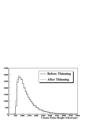
Results are summarised in Table 1 in terms of the relative change of the response before and after back-thinning. Values for the 55Fe data refer to the centroid of the 5.9 keV peak, those for the laser measurements refer to the mean value of the pulse height distribution while those for the 1.5 GeV beam refer to the most probable value of a Landau function fitted to the reconstructed cluster pulse height distribution.
The results of these tests show no significant degradation in the amount of collected charge after back-thinning to 39m and 50 m. 55Fe data shows that the gain is not significantly affected. Instead laser data indicate that the collected charge varied, after processing, by an amount from -16% to +130% with the larger variations observed for longer wavelength. The laser output was monitored using a Si photo-detector and found to be stable to better than 10%. The signal increase could then be explained as a change of the optical properties at the backplane after the thinning process. This effect will be further investigated, but it does not affect the sensor response to a minimum ionising particle. The change observed for the lower wavelength, which is absorbed within the epitaxial layer, is consistent with the measurement uncertainty, due to the stability of the laser source. The ALS data confirm that neither the charge collection nor the signal-over-noise ratio of the detectors for energetic charged particles are affected by the back-thinning process down to thicknesses below 50 m.
 |
 |
3 The CMOS Thin Pixel Pilot Telescope
The batch of thinned Mimosa 5 chips has been used to build a CMOS Thinned Pixel Pilot Telescope (TPPT) installed on the 1.5 GeV ALS BTS facility at LBNL. The ongoing LBNL R&D program on monolithic pixel sensors requires beam tests of sensor prototypes, which are routinely performed at the ALS. But the relatively low energy of the beam extracted from the ALS booster would make it difficult to track particles with enough accuracy to study single point resolution and efficiency of the detector under test, using conventional Si detectors. The TPPT provides a solution to this problem, offering at the same time an interesting prototype CMOS pixel tracker for detailed tracking performance studies towards the ILC Vertex Tracker. This is the first Si beam telescope made of thinned CMOS sensors and consists of three planes of thin pixel sensors (layers 1 to 3), each spaced by 17 mm. One additional Mimosa 5 chip (layer 4) is added 17 mm downstream of the last layer. This detector can be replaced by other detectors under test (DUT) with their independent readout electronics and placed as close as 5 mm from the latest telescope plane. One sector of each chip, corresponding to a 510512 pixel array, is readout through a custom FPGA-driven acquisition board. Four 14 bits, 40 MSample/s ADCs simultaneously read the four sensors, while an array of digital buffers drive all the required clocks and synchronisation signals. The FPGA has been programmed to generate the clocks pattern and collect the sampled data from the ADCs. A 32 bits wide bus connects the FPGA to a digital acquisition board installed on a control PC. Data is processed on-line by a LabView-based program, which performs correlated double sampling and pedestal subtraction, noise computation and cluster identification. To reduce the amount of data written to disk only the addresses and pulse heights of the pixels in a fixed matrix around the centre of a cluster candidate are recorded. The data is converted in the lcio format for offline analysis using a set of dedicated processors developed for the Marlin framework Gaede:2006pj . The telescope is operated in an optical enclosure mounted on an optical rail and aligned on the BTF beam line. The temperature is kept constant during operation at 27∘ by forced airflow. The measured average signal-over-noise for clusters associated to particle tracks is 14.4.
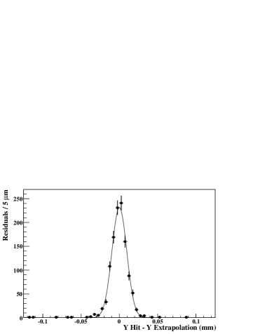
Detailed simulation of the TPPT has been carried out, using the Geant-4 package Agostinelli:2002hh to generate the particle points of impact and energy deposits on the sensitive planes. These have been stored in lcio format and used as input to a CMOS pixel simulation program implemented in Marlin elba06 . The simulation has been validated on beam test data collected with the Mimosa 5 chip on the 1.5 GeV ALS beam and on the 6 GeV DESY beam devis . Noise values have been matched to those measured for the detectors in the telescope. The simulated response has been passed to the same cluster reconstruction program used for real data and reconstructed hits used to fit straight particle tracks, after pattern recognition. The telescope performance has been characterised by the residuals between the extrapolation of a track reconstructed on layers 2, 3 and 4 back to the first layer. Results from simulation have been used for optimising the TPPT geometry. By placing the DUT 5 mm away from the last telescope layer, an extrapolation resolution better than 4 m can be achieved.
Data have been collected at the BTF with different beam intensities ranging from 0.5 particles mm-2 up to about 5 particles mm-2. After data taking, the beam telescope geometry has been surveyed using an optical metrology machine. The results of this survey have been used as starting point of the alignment procedure, performed on a sample of approximately 20000 well-isolated particle tracks with four correlated hits. After alignment, track candidates have been defined by matching hits in the second and fourth layer. Each track candidate has been extrapolated to the third, intermediate layer, where the closest hit has been added if its residual was less than 50 m. The track candidate ambiguities have been solved based on the number of associated hits and on the difference between the track slope and the expected beam slope, determined from the settings of the beam-line final dipoles. Tracks have then been re-fitted using a modified least-square, to account for kinks due to multiple scattering on the measuring planes Lutz:1987vs , and extrapolated to the first layer where the residual to the closest reconstructed hit has been computed. Since the beam contains a fraction of lower momentum particles, which increases while moving away from the beam axis, only the central region of the beam was used and an additional cut was imposed on the residual on the second coordinate. A preliminary result for the residual gives 9.5 m for all accepted tracks, which becomes 9.1 m when restricting to three-hit tracks. This should be compared to 6.8 m obtained from the simulation, which assumes perfect geometry.
Acknowledgements
We thank Marc Winter and Frank Gaede for discussion and Robert Foglia, of Aptek Industries, for assistance with the back-thinning process. This work was supported by the Director, Office of Science, of the U.S. Department of Energy under Contract No.DE-AC02-05CH11231 and used resources of the National Energy Research Scientific Computing Center, supported under Contract No.DE-AC03-76SF00098. We are indebted to the staff of the LBNL Advanced Light Source for their help and the excellent performance of the machine.
References
- (1) S. Kleinfelder et al., Nucl. Instrum. and Meth. A 565 (2006), 132.
- (2) W. Dulinski et al., Nucl. Instrum. and Meth. A 546 (2005), 274.
- (3) Yu. Gornushkin et al., Nucl. Instrum. and Meth. A A 513 (2003), 291.
- (4) G. Deptuch, Nucl. Instrum. and Meth. , A 543 (2005) 537.
- (5) Aptek Industries, San Jose, CA 95111, USA.
- (6) F. Gaede, Nucl. Instrum. Meth. A 559 (2006) 177.
- (7) S. Agostinelli et al., Nucl. Instrum. Meth. A 506 (2003), 250.
- (8) M. Battaglia, to appear on Nucl. Instrum. Meth. A (2006).
- (9) D. Contarato et al., Nucl. Instrum. Meth. A 565 (2006), 119.
- (10) G. Lutz, Nucl. Instrum. Meth. A 273 (1988) 349.