Pixel Vertex Detectors
Abstract
Pixel vertex detectors are THE instrument of choice for the tracking of charged particles close to the interaction point at the LHC. Hybrid pixel detectors, in which sensor and read-out IC are separate entities, constitute the present state of the art in detector technology. Three of the LHC detectors use vertex detectors based on this technology. A development period of almost 10 years has resulted in pixel detector modules which can stand the extreme rate and timing requirements as well as the very harsh radiation environment at the LHC for its full life time and without severe compromises in performance. This lecture reviews the physics and technology of pixel detectors for tracking and vertexing at the LHC.
I Introduction
I.1 From gas-filled wire chambers to pixel vertex detectors
Advances in particle tracking have always lead to breakthroughs in experimental methods and hence to a new quality of experiments. A prominent example of this statement is the Nobel-awarded invention of the multi-wire proportional chamber by G. Charpak in 1968 charpak1 ; charpak2 , which for the first time allowed the electronic detection of particle tracks to an accuracy in the order of a mm and below. Later (1975) spatial resolutions in the order of 100 were obtained with drift chambers. These detectors typically had a readout density of 0.05 channels/cm2. So called vertex drift chambers (see e.g. jaros ) improved the resolution of such chambers down to about 50 with a readout density of 0.1 channels/cm2. These devices enabled the detection of decay vertices, and hence measurements of the life times of long lived (ps) particles.
Silicon micro strip detectors were developed in the early eighties hyams . With this new type of detectors spatial resolutions in the order of 10 became accessible for the first time. The identification of secondary vertices and and hence of particle life times became precision measurements. These devices had a channel density of the order of 100 channels/cm2.
Pixel detectors pixelbook , finally, belong to this category of instruments leading the way to a new frontier in measurement techniques and hence in physics. At the LHC, close to the interaction point, no other detector instrument is capable to cope as well with the high density and rate of particle tracks and stand the fierce radiation environment. There is no large improvement in spatial resolution when comparing to strip detectors, however pixel detectors return true 3D space points, a necessity for pattern recognition and tracking in the LHC environment near the interaction point. The channel density increases by more than an order of magnitude compared to strip detectors to about 5000 channels/cm2. Fast readout of such a large (in terms of channels) and complex system required new technologies and methods, which have been developed during the past decade and are subject to this lecture.
I.2 Tracking detectors at the LHC
At the LHC with a center of mass energy of 14 TeV on average 22 interactions with 1200 tracks occur during one bunch crossing every 25 ns. This is a track rate of 50 GHz, about 106 times the track rate that LEP encountered. The total particle fluence is 1015 neq/cm2 over a projected 10 year life time at the LHC, where the damage created by the charged and neutral particles, mostly pions and protons near the IP, has been normalized to the equivalent of the damage of 1 MeV neutrons (neq). This fluence of particles causes lattice damage by collisions with the lattice atoms (non-ionizing energy loss), but also by ionization of atoms which corresponds to a total dose of 600 kGy in 250 silicon bulk material assuming minimum ionizing particles (mips).
Pixel detectors are most important for the following measurement tasks, in the order of importance
Sketch of a secondary vertex which is displaced from the primary vertex. The impact parameter is defined as the perpendicular distance of closest approach of a track to the primary vertex and has a positive sign if it lies in the same hemisphere as the track, otherwise the sign is negative.
-
1
Pattern recognition and tracking
Precision tracking points are provided in three dimensions which can be used as precise seeds for the reconstruction of tracks. With respect to this task a pixel layer is probably as valuable as 3 to 4 layers of microstrip detectors which need x,y as well as u,v strip orientations to resolve the ambiguities existing in an environment with many tracks per uni area.
-
2
Vertexing (primary and secondary vertex, see Fig.1)
The ATLAS inner detector for example projects the following performance values
-
-
impact parameter resolution: 10m (r), 70m (z)
-
-
secondary vertex resolution: 50m (r), 70m (z)
-
-
primary (main) vertex resolution: 11m (r), 45m (z)
-
-
(life) time resoution: 70 ps
The impact parameter (c.f. Fig. 1) resolution in ATLAS is given by
-
-
-
3
Momentum measurement
For ATLAS the expected momentum resolution obtained with the complete Inner Detector is
Idealized two layer detector. marks the interaction point. is the extrapolated interaction point of the track at the IP (impact parameter). (a) configuration assuming an ideal layer 2 (=0), (b) configuration assuming an ideal layer 1 (=0).
In order to assess which are the important parameters for a micro vertex detector, a simple 2-layer detector example already provides the most important insights. Consider in Fig. 2 configuration in which first the outer layer, detector-2 is assumed to have perfect resolution (=0, Fig. 2(a)). The impact parameter error of the track is thus determined by , the resolution of the first layer and the aspect ratio of the two layers
Reversing now the situation and assuming that the first layer has perfect resolution (=0, Fig. 2(b)) yields
Adding the two contributions to in quadrature and adding also a term for multiple scattering yields
from which it is obvious what to pay attention to for vertexing: the innermost layer of a vertex detector must be as close to the IP as possible, the resolution () of this innermost layer is most important, and the material measured in radiation lengths must be as little as possible, because .
Simulated event of the reaction pp ttH, H bb, tt W(l)b W(qq)b at the LHC. Also shown are the positions of the ATLAS silicon tracking detectors: pixels and SCT.
Figure 3 shows a simulated event of the reaction pp ttH, which demonstrates again the importance of 3D-hits from pixel detectors for track reconstruction.
The inner tracking systems of ATLAS, CMS and ALICE all employ semiconductor detectors, as the event rate and complexity does not allow large volume gas-filled detectors which were still the best suited tracking detectors for experiments at LEP and SLC. Some essential parameters of the tracking systems are give in Table 1.
| points | (r) () | (Rz) () | area (m2) | ||
| ATLAS | pixels | 3 | 10 | 60 | 1.8 |
| SCT | 4 | 17 | 580 | 60 | |
| TRT | 36 | 170 | – | 300 equiv. | |
| CMS | pixels | 3 | 10 | 20 | 1 |
| strips | 10 | 23 - 52 | 23 - 52 | 200 | |
| ALICE | pixels | 2 | 12 | 100 | 0.2 |
| Si-drift | 2 | 38 | 28 | 1.3 | |
| strips | 2 | 20 | 830 | 4.9 |
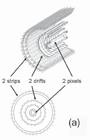
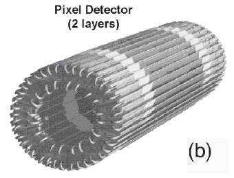
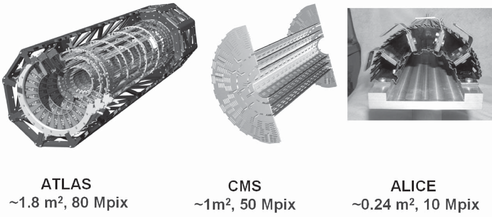
The ATLAS inner detector has three systems: a 1.8 m2 pixel detector, a semiconductor tracker (SCT) consisting of Si micro strip detectors of about 60 m2 and a transition radiation tracker (TRT) made of individual straw tube, providing on average 36 points on a track. The pixel detector comes as 3 barrel layers and 3 disks on either side. It has a total of about 8 107 pixels with dimensions of .
The ATLAS Inner Detector (a) has a pixel detector, a semiconductor tracker (SCT) and a Transition Radiation Tracker (TRT). The pixel detector (b) consists of 3 barrel layers and 23 disks.
The CMS Inner Detector (a) has a pixel detector and a large Si-microstrip tracker. The pixel detector (b) consists of 3 barrel layers and 22 disks.
The ALICE Inner Detector has a large TPC (not shown) plus a silicon tracking system consisting of (a) a pixel detector (PD), a siicon drift detector (SDD) and a Si-Strip detector (SSD). The pixel detector (b) consists of 2 barrel layers and no disks.
CMS has a large all silicon tracker, composed of a pixel detector with 3 barrel layers and 22 disks (1m2) and a 200 silicon microstrip detector with 10 measurement points. The pixel detector has 3.3 107 cells with dimensions of 100150 . Drawings are shown in Fig.5. ALICE, finally, has two layers each of different technologies kotov2006 , pixels, Si drift detectors, and Si strip detectors as shown in Fig. 6.
II Hybrid Pixel Detectors for the LHC
II.1 The pixel detector principle
Figures 7(a) and (b) show the principle of the hybrid pixel technology. A pixellated silicon pn-diode as sensor and a readout chip, 1-1 corresponding in every pixel cell, are connected via tiny conductive bumps using the bumping and flip-chip technology. A traversing particle creates charges (electrons and holes) in the sensor by ionization. Separated by the electric field applied to the sensor, the movements of negative and positive charges induce a signal on the pixel electrode above (and may be also on its neighbors). The signal is amplified, discriminated and digitized by the electronics circuitry in the pixel cell of the chip and is then transmitted to the periphery.
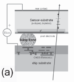
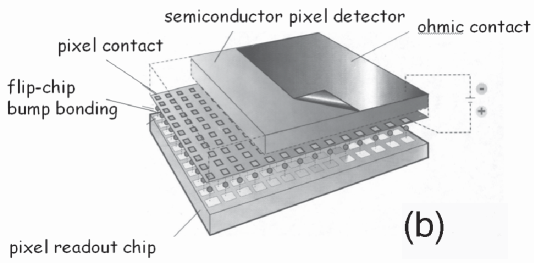
The hybrid-pixel concept. (a) one pixel cell showing the charge collecting sensor on top and the signal amplifying circuitry on the bottom, both connected by a bump connection.
The detection principle is - with one peculiarity, explained below - the same as that of a pn-junction in reverse bias (Fig. 8). The characteristic distribution of the space charge is directly derived from the neutrality condition
| (1) |
in which , are the number of acceptors and donors, respectively, and , denote the coordinates of the space charge boundaries. Assuming an abrupt transition between n and p regions this results in a rectangular shape of the respective space charge regions with a constant charge density. The electric field and the built-in potential result from two integrations of the first Maxwell equation
| (4) | |||||
| (5) |
with a linearly rising and falling electric field with its maximum at .
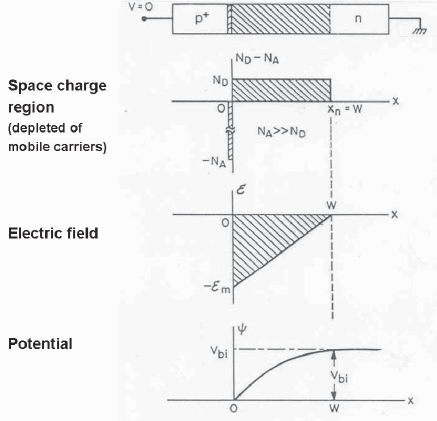
Characteristics of a reverse biased abrupt pn-junction: space charge, electric field and potential distributions.
In the case of a particle detector the doping of one side of the junction, say the p-side, is very high (1019 cm-3), while the n-side is lightly doped (1012 cm-3). The depletion region thus basically grows from the junction into the more lightly doped bulk. With an additional reverse bias voltage Vext = Vdep + V, where Vdep is the depletion voltage, the electric field becomes
| (6) |
The depletion depth d is proportional to the square root of the applied external voltage
| (7) |
and the electric field falls linearly from the front to the back. Normally sensors are operated with in over-depletion resulting in a non-zero field at the back side which is beneficial for a fast charge collection (see Fig. 9(a)). The capacitance of the device can be treated as a parallel plate capacitor
| (8) |
and grows inversely propostional to . This allows to determine the full depletion voltage from a capacitance measurement as shown in Fig. 9(b).
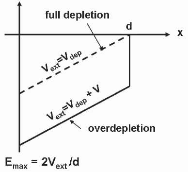
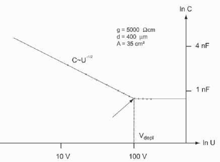
(left) Linear shape of the electric field of a silicon detector in full depletion (dashed line) and in over-depletion (full line). (right) Determination of the full depletion voltage by measuring the capacitance.
II.2 The signal
Although in silicon the band gap is 1.1 eV, 3.61 eV are needed on average to create one e/h pair as energy is also absorbed into phonons. A minimum ionizing particle hence creates by energy loss 80 e/h pairs per path length and 20000 e/h in a 250 thick fully depleted sensor, corresponding to a total charge of about 3 fC. Note that pixel sensor are also suited to detect radiation: a 10 keV X-ray photon, when absorbed, generates about 3000 e/h pairs or 0.5 fC. The generated charges are separated by the electric field inside the sensor and drift with drift velocity , where x is the depth coordinate, towards their respective electrodes. The charge cloud widens with time by diffusion while it drifts to the electrode. The gaussian width of the diffusion cloud is given by , where D 36 cm2s-1 is the diffusion coefficient of silicon. This leads in typical sensor thicknesses of 250 and with typical electric fields and drift velocities (5mm/ns) to drift times of about 10 ns and cloud widths in the order of 8-10. For pixel detectors the electrode on one side (usually the one that collects electrons, n+, see section III.2) is segmented into pixels with a typical size of (CMS) or (ATLAS and ALICE). The charge cloud therefore spreads at most over 2 pixels, 4 pixels if a corner of 4 pixels is hit. Note that for photon detection sensor materials with a high Z, such as Cd(Zn)Te or HgI2 are desirable, due to the dependence of the photo effect Z4-5, where the exponent changes with the photon energy.
A permanent nuisance in the ionization process for experimentalists is the appearance of electrons, high energy knock-on electrons. electrons follow a 1-1 relation between their kinetic energy and their emission angle
| (9) |
where T denotes the electron’s kinetic energy with kinematically maximally possible value Tmax = 2mc2. = is the Lorentz variable and m the electron mass. This relation is a very steeply falling function: high energetic electrons (compared to the energy of the projectile particle) are emitted in the forward direction and slow, highly ionizing () electrons are emitted a right angles. The angular distribution is
| (10) |
where D=0.3071 MeV g-1cm2 is a constant, z the charge of the projectile and Z, A, , x are charge and mass number, density and thickness of the traversed matter. This function peaks very steeply by orders of magnitude at angles close to 90∘. Therefore, as a rule of thumb, -electrons are almost always emitted under right angles and are highly ionizing. The effect of a electron emission in a silicon pixel detector is sketched in Fig. 10. A 100 keV electron occurs in 300 thick silicon with 6 probability and has a typical range of 60 . Hence it created about 4500 e/h pairs along its path, perpendicular to the parent particle. This causes several neighbor pixels to fire. The reconstructed ’hit‘’ will thus be systematically shifted to the side of the electron emission.
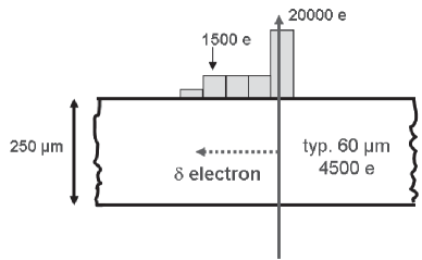
Effect of a hit mis-measurement that electrons can cause in a pixel detector.
As mentioned before the signal on the electrodes is induced by the movement of the separated charges in the electric field inside the sensor. This is generally described by the Ramo theorem Ramo as
| (11) | |||||
where and are the current resp. charge induced on the electrode by the movement of the electrons and holes, q is the moving charge, the velocity of the movement and and are the so called weighting field resp. weighting potential. They have nothing to do with the electric field and potential inside the sensor, but rather determine how the charge movement couples to a specific electrode. The weighting field can be calculated by setting the potential of the electrode under consideration to 1 (or 1V) and all other electrodes to 0 (0V) as indicated in Fig. 11(a).
(a) How to calculate the weighting potential/field in a multi electrode configuration. (b) Weighting potential in a simple 2-electrode configuration, e.g. a parallel plate detector or an area diode. (c) Current signals as a function of time in a 2-electrode configuration.
In a 2-electrode configuration (e.g. an area diode) the calculation is rather simple: set the top electrode of the sensor to V=1 and the bottom electrode to V=0. The formulae for weighting field and potential thus are
| (12) |
as shown in Fig. 11(b) and the current induced on the readout electrode reads
| (13) |
with the electric field given by eq. 6 with time dependent x(t). Then solving eq. 13 we receive the characteristic exponential shape of the current with time, which reflects the drift velocity change with time (here for the electron signal)
| (14) |
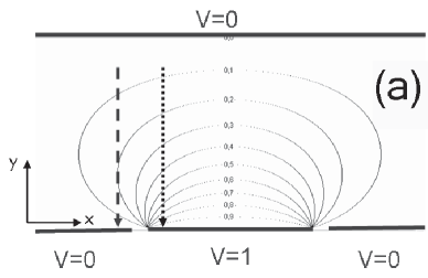
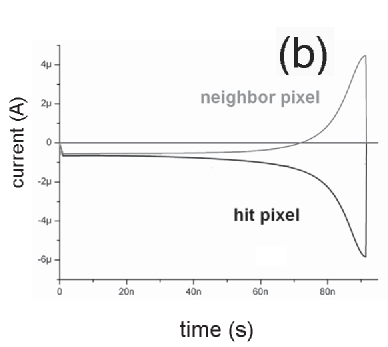
(a) Weighting potential in a strip/pixel geometry (1-dim) together with two different paths of charge movement, one arriving at the readout electrode, the other arriving at the neighbor electrode, (b) current signals for the two different charge drift paths showing the ’small pixel effect‘.
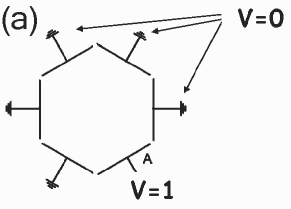
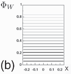
In a configuration with segmented electrodes like in a pixel detector some caution is necessary. Figure 12(a) shows the ansatz to calculate the weighting potential, and the result in one dimension. The not easy calculation to solve the Poisson equation using the Schwarz-Christoffel conformal transformation conformal yields
| (15) |
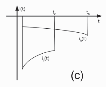
where and are the coordinates and is the pixel width. The form of the weighting potential is shown in Fig. 12(a). Also shown are two parallel drift trajectories, one ending on the electrode considered (dotted arrow) and the other on the neighbor electrode (dashed arrow). The corresponding current signals are displayed in Fig. 12(b). For both pixels initially the current signals are identical, independent of the electrode which eventually collects the charge. While the trajectory of the hit pixel, however, shows a rapidly increasing (negative) current signal when approaching the electrode, the signal of the neighbor trajectory crosses the zero line and then goes positive resulting in a vanishing net integral of the pulse (i.e. the total charge). Most of the signal is induced on the pixel electrodes only shortly before the drifting charge cloud arrives at the pixel (small pixel effect).
Finally, pixel detectors at LHC are operated in magnetic fields (2T for ATLAS, 4T for CMS). In a B-field the drift motion of the charge clouds is on a circle. This motion is stopped on average after one mean free path length of the drifting electrons, resulting in a complicated path which can be described by an effective motion towards the readout electrode under an angle , the Lorentz angle, as
| (16) |
where is the Hall mobility, which differs by a factor 1.15 (0.72) from the normal mobility for electrons (holes). The Lorentz angle has been measured Lorentz-ATLAS ; Lorentz-CMS in ATLAS (2T field) to be -15∘ before irradiation with 150 V depletion voltage, and to -5∘ after irradiation with 600 V depletion voltage, respectively. This difference is mostly due to a decrease of the mobility with increasing electric field inside the sensor. Note that the effective incidence angle to the electrode is given by the sum of the Lorentz angle and the tilt angle, by which the pixel modules are tilted out of the perpendicular plane. This tilt angle in ATLAS is +20∘.
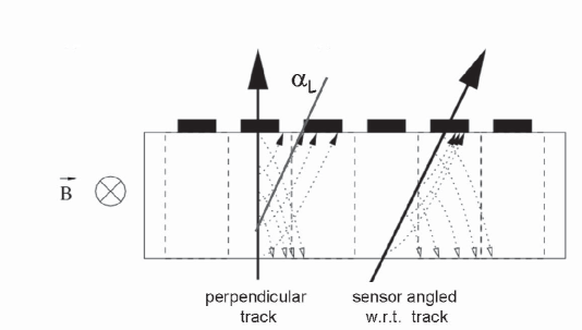
Drift of charges in a pixel detector under the effect of e perpendicular magnetic field. The drift occurs under an angle , the Lorentz angle.
II.3 The noise
For noise considerations in detector and electronics readout configurations it is important to consider the following physical noise sources
-
-
number fluctuations of quanta, which lead to 1. shot noise and 2. 1/f noise
-
-
velocity fluctuations of quanta which lead to 3. thermal noise.
Shot noise is generated when charge quanta are emitted over a barrier, as is the case in a diode. Thermal noise occurs from statistical thermal motion of charge carriers, here inside the transistor channel of the amplifying transistor. 1/f noise in a FET has its physical origin in the trapping and releasing of charge carriers in traps in the Si-SiO2 interface of the transistor channel.
Where do these noise sources appear in a typical pixel detector readout chain (cf. Fig. 14) ?
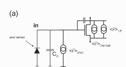
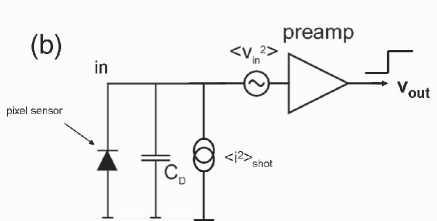
(a) A typical charge integrating pixel detector readout, represented here by a single amplifying FET and the three main noise sources: shot noise from detector leakage current, and thermal as well as 1/f noise in the transistor channel. (b) Transistor thermal and 1/f noise is treated as serial voltage noise at the input of the preamplifier.
Using the current noise source inside the transistor channel can be regarded as a voltage noise source in series at the input of the amplifier (c.f. Fig. 14(b)). The noise sources then can be written as
-
-
series thermal voltage noise
(17) -
-
series voltage 1/f noise
(18) -
-
and parallel current shot noise
(19)
with
f = frequency
k = Boltzmann constant
T = temperature
gm = transconductance of the amplifying transistor
Kf =
1/f
noise coefficient = 3-4 10-32 C2/cm2 for n-channel MOSFETs
W, L = width and length of the transistor gate
Cox = gate
oxide capacitance
q = elementary charge
ileak = detector leakage
current
It is customary for charge integrating devices to express the noise voltage output as an equivalent noise charge ENC, i.e. the charge one would need to see at the input that produces the observed output noise voltage
| (20) |
with the relation
| (21) |
The charge integrating amplifier transforms the noise input into an output voltage, which depends on the feedback- , input- and load- capacitances, as well as on the characteristic feedback time constant pixelbook .
| (22) | |||||
If - as is often the case (see Fig. 15) - an additional filter amplifier (shaper) is the bandwidth limiting element and not the preamplifier, the latter can be neglected in the noise calculation. The shaper consists of a sequence of bandwidth limiting elements, in the most general case N high pass stages and M low pass stages (see Fig. 15). The equivalent noise charge behind the shaper is then given by pixelbook
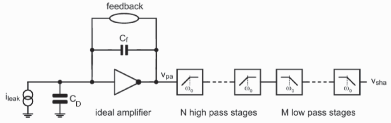
Pixel detector readout with a charge integrating preamplifier and a filter amplifier (shaper).
Note that the noise depends on three important quantities to which attention has to be paid to: the sensor leakage current and the shaping time , both of which increase the parallel shot noise contribution, and the total input capacitance, dominated by the detector capacitance CD, which increases the two parallel noise components (thermal and 1/f). The shaping time decreases the thermal noise which results in the fact that the three noise contributions to the detector/readout configuration have a minimum at an optimum shaping time , as is sketched in Fig. 16.
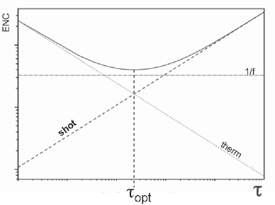
The three noise contributions (thermal, 1/f and shot noise) as a function of the shaping time in a logarithmic representation. The dependence results in a minimal total noise at an optimal shaping time.
Pixel detectors have the advantage of small input capacitances in the order of several hundred fF and thus have the potential of being low noise devices. Typical figures for LHC pixel detectors are
| noise | = 150 e- | initially | |
| = 200 e- | after 10 years at LHC | ||
| signal | 19500 e- | total charge in 250 silicon | |
| = 13000 e- | including charge sharing between pixels | ||
| = 6000 - 8000 e | after 10 years at LHC |
hence guaranteeing a S/N ratio of more than 30 throughout the LHC lifetime.
III Making a Pixel Detector
From the pixel sensor to the module-ladder
The particle fluence that pixel detectors at 5cm distance from the IP at LHC have to expect during 10 years of operation is about 1015 neq/cm2. This fact constitutes enormous challenges to pixel sensors, which develop large leakage currents and need high voltages for full depletion, as well as to the front end electronics, which suffers from threshold shifts and generated parasitic transistors; but also to the mechanic elements whose material performance degrades, glue becomes brittle, etc. This has required intensive irradiation tests over many years.
III.1 Hybrid Pixel Assembly
A so called bare pixel module consists of the pixel sensors and a number of electronics chips for amplification and readout (16 in the case of ATLAS and CMS, 5 for ALICE) which are mated by means of the bumping and flip-chipping technology (IZM1 ; Fiorello and pixelbook ). In the case of ATLAS the 10 cm sensor wafer has three 2.1 x 6.4 cm2 sized sensor tiles. The 20 cm chip wafer instead has 288 7.1 x 11.4 mm2 sized front end chips which have been tested to be functional with an average yield of 82. The mating is done in part with indium bumps Fiorello or solder bumps IZM1 ; IZM2 . Each chip has about 3000 such bumps. The chip wafers are thinned by backside grinding after bumping from initially about 800 thickness down to 180. Figure 17 shows a bare module after assembly and a cut through a bump row, which nicely shows the module after the mating process (here solder). The bumps in case of Indium are about 7 high and are applied on both, sensor and chip wafer. After thermo-compression the remaining thickness is about 10. Solder bumps are applied only to the chip wafers and are 25 in diameter, and about 20 after flip-chip and reflow (see Fig. 17).
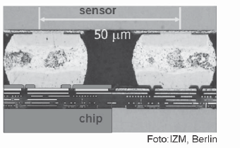
(Left) components of the ’bare‘’ module are the sensor, several FE-chips and the interconnection between them. (Right) a cut through the bump row showing the bumps and the metal layers of the chip electronics.
To produce a fully functional module, additional assembly steps are necessary as shown in Fig. 18. The output lines are connected via wire bonds to a flex-kapton hybrid foil with fine-print lines. The signals are routed to a further chip, the module control chip MCC and from there through another flex component (pigtail) to the micro cables which run to the electro-optical interface which is in ATLAS between about 20 cm and 120 cm away from the module. Figure 18 also shows a CMS-pixel module, fully assembled.
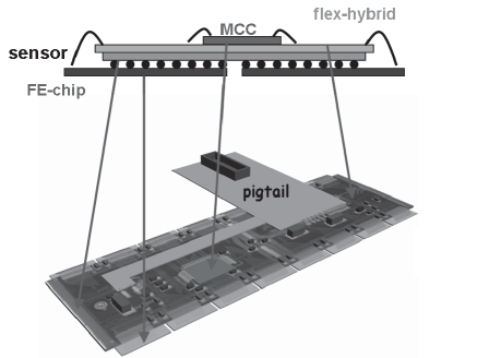
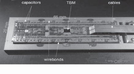
(Left) Sketch of the composition of a complete ATLAS module, including sensor and FE-chip connected by bump bonds, a FLEX hybrid kapton foil and the module control chip MCC. The ‘pigtail ’ provides the connection to the outside; (Right) Photograph of the CMS Pixel Module.
III.2 Pixel Sensors in the LHC radiation environment
The intense radiation at LHC requires dedicated designs for both sensor and FE-chip. For the sensor, mostly the non-ionizing energy loss which produces non-reversible lattice damage is important in this respect. Figure 20(a) sketches the main defect appearances. We distinguish so called point defects and defect clusters, the latter originate from damage that a recoiling lattice atom can cause. The size of the clusters typically is 10 nm 200 nm. For pixels sensors the largest concern comes from double vacancies and interstitials, both producing generation/recombination levels deep in the band gap which lead to an increase of the leakage current, and therefore to higher noise (see eq. 19). Also the effective space charge in the depletion region is changed leading to an increase of the effective doping concentration and as a consequence an increase in the necessary voltage for full depletion.
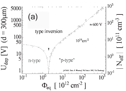
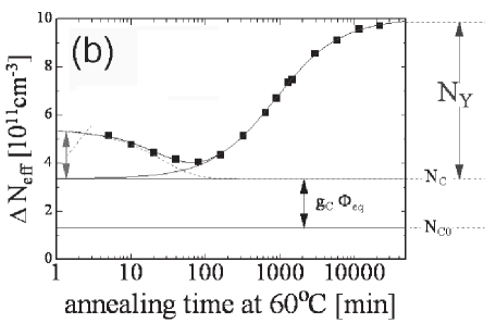
(a) Change of the effective doping concentration with fluence showing type inversion; (b) Annealing of irradiation damaged sensors with time showing the beneficial annealing at the start and the reverse annealing at longer time scales.
This is shown in Fig. 19(a), where the effective doping concentration as well as the full-depletion voltage are plotted as a function of the fluence. Neff first decreases to zero and then becomes almost intrinsic at a fluence of 2-5 1012 cm-2. It then rises again (type inversion) rwu . The effective doping concentration after irradiation damage also changes with time as shown in Fig. 19(b): beneficial annealing occurs at short time scales, so-called reverse annealing at longer time scales lindstroem01 . The latter is suppressed when keeping the damaged sensors at low temperatures below the freezing point. At -10∘ C the time constant for reverse annealing is about 500 years, while at +20∘ C it is only about 500 days moll2006 .
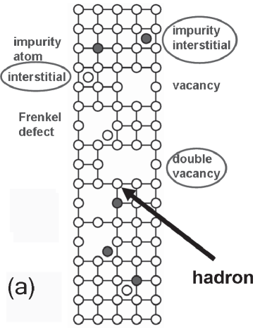
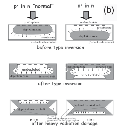
(a) Sketch of some damage processes that hadrons can cause to a lattice; (b) the effects of radiation damage to ‘p in n ’ (left) and to ‘n in n ’ sensors (right) in comparison.
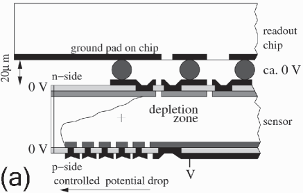
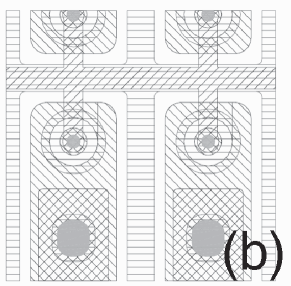
Finally, trapping centers are being created which can trap the signal charge and thus lead to a loss in signal. Solutions to irradiation damage in silicon have been found through intensive RD, most notably by the CERN RD48 and RD50 collaboration lindstroem01 ; moll-nimb ; eremin ; moll-current . For the fluences expected at LHC in the pixel detector oxygenated float zone silicon has proven to stand the expected irradiation from protons and pions within the operation specs of the detectors (e.q. 600 V maximum bias voltage), while for neutrons which produce less point defects but more cluster defects this is not the case. Close to the interaction region, however, particle fluence by pions is dominant. The pixel sensor design has also been adapted to the development of the effective doping concentration with increasing fluence by chosing n+ pixel implants on lower doped n-bulk material. Figure 20(b) shows the development of the depletion region for p+ in n and for n+ in n pixel sensors in comparison. The depletion zone grows from the higher doped p-region into the lower doped n-bulk, in the presence of type-inversion under irradiation. While. after type inversion, for the standard p in n sensors the depletion region grows from the non-pixellated bottom, which requires to always operate under full depletion, for n in n sensors after type inversion the depletion region grows from the electrode (i.e. pixel) side. This allows operation also without full depletion which might be unavoidable after several years of LHC-running. At the n-pixel n-bulk interface at the top, measures are taken to prevent the electron accumulation layer, which develops a the Si-SiO2 interface where there is no intrinsic depletion zone as is the case for a pn interface. Figure 21 shows the different advantages and disadvantages of isolation measures using either p-stop implants between the n-implants, or a lighted doped boron p-spray in the entire region between implants. The highest fields occur always at the lateral pn junctions. Irradiation increases the oxide charges and also the substrate doping, such that the backside bias must be increased after irradiation. This generally increases also the maximum field with irradiation. For the p-spray situation the sensor develops high fields initially. The concentration of the shallow p-layer can be chosen such that when the oxide charges go into saturation the p-spray layer goes into depletion which results in a decrease of the fields with irradiation. Finally, the moderated p-spray, i.e. p-spray with a doping profile, keeps the best of both worlds rar96 .
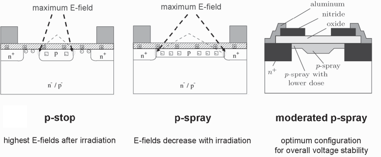
Isolation measures at the n+n interface: left p-stop, center p-spray, right moderated p-spray.
Figure 22(a) shows the edge of a pixel module. As the edge of the sensor is conducting the backside bias voltage must be brought to 0V by a voltage dividing guard ring structure. Otherwise the risk of discharge is present over the small gap between sensor and chip. In normal operation the sensor pixels have a defined potential by contact to the FE-chip. For testing purposes of the sensor, however, before bonding has been done, this is not the case. This problem has been overcome by introducing a bias grid which runs around all pixels (see Fig. 22(b)). Applying the punch through voltage to the grid via an external contact, all pixels are brought to a defined potential by the punch-through effect (more details can be found in pixelbook ).
(a) Edge of a pixel module showing the controlled potential drop from the bias voltage to 0V via a series of guard rings; (b) punch-through biasing of pixel implants by means of a bias grid supplying every pixel.
The bias grid of course produces additional implants in the pixel cell which lead to a reduced charge collection efficiency in this region by some 10-20. This is however tolerable in expense for being able to thoroughly test the sensors before module assembly.
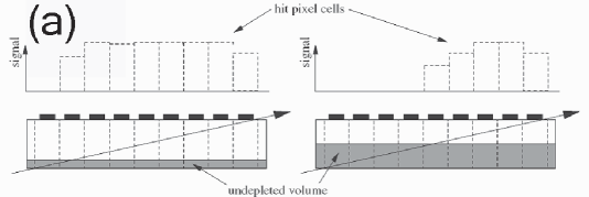
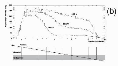
Pixel detectors offer a nice way of measuring the depletion depth after irradiation by exposing them to particle beams under a steep angle of inclination, the shallow angle method rohe-CMS . This is illustrated in Fig. 23(a). The observed cluster size is a direct measure for the depletion depth. Figure 23(b) shows the measured cluster size for different bias voltages for CMS pixels, which correspond to fully and less depleted pixel sensors. Full depletion after irradiation is only obtained for bias voltages of more than 450 V.
(a) Shallow angle method to measure the depletion depth of a pixel sensor after irradiation. (b) observed cluster size under shallow incidence angle, showing the dependence of the cluster size on the depletion state of the sensor.
Trapping effects due to irradiation can also be measured using the shallow angle method as the track passes the pixel cells in a varying depth andreazza2006 . If trapping occurs, the collected charge depends on the distance of the track passage to the pixel electrode.
III.3 The pixel front end chip
The pixel front end chips of ATLAS, CMS and ALICE are all fabricated in the 0.25 CMOS technology. The cell sizes of ATLAS and ALICE are 50400 while CMS has 100150 . In the case of ATLAS the chip blanquart03 ; blanquart01 is organized in 18 columns time 160 rows, in total 2880 pixel cells, which are processed in parallel. The readout is zero-suppressed. A block diagram of the functionality is shown in Fig. 24. The current signal of a hit is integrated by a charge sensitive preamplifier, whose feedback capacitor is discharged by a constant current. This results into a triangular pulse shape. The pulse then runs through a discriminator which issues a norm pulse whose length is determined by the times at which the rising and the falling edges of the input cross the discriminator threshold. The length of the output pulse is thus a measure of the time over threshold (ToT) which in turn is a measure of the total charge. The address of the pixel cell and the time stamps are stored into RAM storage at the periphery. A fast scanner through a double column picks up the valid hit addresses and time stamps and stores them into buffers at the bottom of the pixel columns where they remain waiting for the ATLAS first level trigger. The hits are removed from the buffers if no trigger occurs in coincidence with the time stamps. If the trigger time agrees with the time stamp a hit is read out. Requirements to the front end chip are that the noise hit rate be kept small compared to the real hit rate. It is demanded that the quadratic sum of the noise value and the spread of the thresholds over the chip be more than a factor of five below the chosen threshold. For a nominal threshold setting of 3000 e- this means less than 600 e-. The obtained noise figures are in the order of 50-60e-. The untuned threshold dispersion is 600 e-. It is possible to tune (correct) the threshold settings by a 7-bit digital trim DAC. After tuning the dispersion is drastically reduced however to values much lower than 100e-, thus easily meeting the above requirement. The functional blocks of the CMS Pixel chip erdmann03 ; baur-CMS are similar. However, CMS additionally stores the analog pulse height in a sample and hold stage, i.e. have a direct analog readout, while the ATLAS readout is analog through the ToT trick. In CMS the amplitude as well as the row and column addresses are then coded in analog levels.
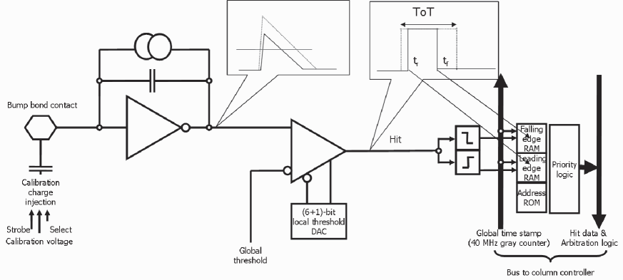
Functional block diagram of the ATLAS pixel front end chip FEI3 (see text).
Figure 25 shows the overlay of 4160 pixel readouts in the CMS system Kaestli2005 . Every event starts with an ’ultra black’ followed by seven clock cycles, five of which encode 13 bits for the pixel address. The analog pixel pulse height then follows in the seventh clock cycle.
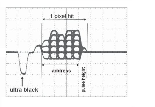
Analog encoding of a hit in the CMS Pixel Detector displayed here by overlying 4160 readouts (after Kaestli2005 ). After an ’ultra black’ five clock cycles encode in analog levels 13 bits for the pixel address. The analog pulse is transmitted with the following clock cycle.
III.4 Radiation effects in the front end electronics
The radiation effects that pixel chips suffer from differ from those already described for the pixel sensors. For CMOS chips it is mostly the ionizing radiation that generates positive charges in the SiO2 and also creates defects in the Si-SiO2 interface as shown in Fig. 26(a). The mobility of electrons (high) and holes (low) is vastly different in SiO2 such that charge pairs created by ionization produce low mobility positive charges in the gate oxide while the electrons have escape. This creates a net positive oxide charge and as a consequence a shift in the transistor threshold. Another effect is the generation of leakage currents under the field oxide, which in effect creates parasitic unwanted transistors. Both effects have been much reduced since so-called deep sub-micron CMOS technologies have become available for HEP customers. The thin gate oxide (5nm in 0.25 CMOS) arranges for the low mobility holes to tunnel out, thus curing or at least reducing the effect of threshold shifts (see Fig.26(b,top). Transistor leakage currents can be eliminated by designing transistors with annular gate electrodes and additional guard rings as is also shown in Fig. 26(b).
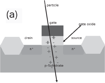
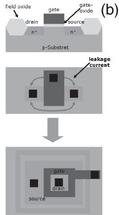
(a) Effect of ionizing radiation on the performance of CMOS ICs. Positive oxide charges lead to transistor threshold shifts; (b) thin gate oxide in deep sub-micron technologies as well as annular transistors cure the main irradiation problems of CMOS ICs.
Also the digital parts of the front end electronics are affected by the radiation at LHC. Most prominently radiation induced bit errors, so called ’single event upsets’ (SEU) are reasons of concern. Large amounts of charge on certain circuit nodes, created for instance by nuclear reactions or high track densities can cause a bit-flip. Two examples of more error resistant logic cells are given in Fig. 27. A capacitance between input and output node (Fig. 27(a)) slows down the response time and makes the standard SRAM cell more tolerant against short charge glitches on the input as long as the critical charge value Qcrit = Vthresh C is not crossed. The CMS ROC chip uses such protections. The ingenious DICE SRAM cell (Fig. 27(b)) stores the information and its inverse on 2+2 independent and cross-coupled nodes, such that a temporary flip of one node cannot permanently flip the cell. Such a cell is used in the ATLAS FE-chip on sensitive nodes.
(a) Standard SRAM cell made more SEU tolerant by introducing a capacitance between input and output node. (b) The SEU tolerant DICE SRAM cell.
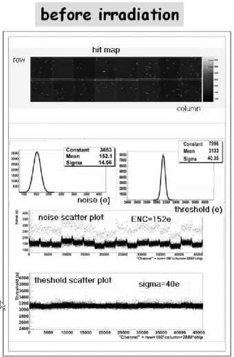
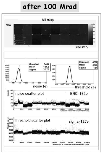
Pixel modules have been irradiated to 10-year LHC doses and beyond. Figure 28 shows the comparison of an ATLAS pixel module with 16 chips before and after irradiation to 1 MGy or 2.5 10 p/cm2 which, in fact, corresponds to a total dose of about 20 years at LHC. The figure shows on the top a hit map and below distributions of the measured noise and the thresholds determined by respective threshold scan measurements. It can be noted that while the noise and threshold distributions vary more from chip to chip, which can be seen in the bottom scatter plots, the quadratic sum of their averages still remains well under 300, i.e. comfortably away from the nominal threshold setting of 3000. The spatial resolution of irradiated modules decreases by about 40 and the in-time hit efficiency - the efficiency of hit detection within the 25 ns time window of the LHC bunch crossing - decreases from 99.9 before irradiation to 97.8 after 600 kGy.
III.5 Support structures and material issues
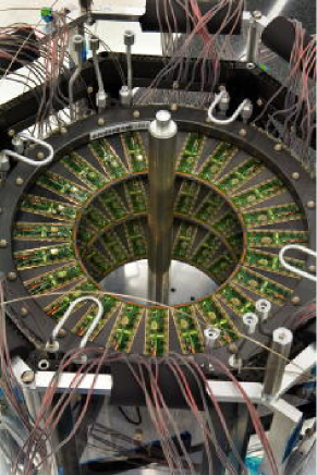
The pixel modules are loaded on ladders and disks to complete the detector. The main goal for detector builders in this respect is to minimize the amount of material in terms of radiation length imposed by the support structure and the cooling mechanics, which is particularly difficult to achieve when the operation temperature is required to be about -5∘ to -10∘ C in order to block the reverse annealing effect (see chapter III.2). Figure 29 shows the mechanical support structures of the pixel detectors for ATLAS, CMS and ALICE.
In central heavy ion collisions, the environment of the ALICE detector, up to 8000 charged particles per unit of rapidity are produced, generating hit densities of about 80 hits / cm2. As the luminosity for heavy ion collisions is much smaller than for pp collisions (L 1027 cm-2 s-1 for Pb-Pb collisions, L 1029 cm-2 s-1 for Ar-Ar or O-O collisions) the radiation levels are only 5 kGy or 61012 neq / cm2. Hence, operation at temperatures below zero to suppress the reverse annealing effect, are not mandatory. Instead, operation at room temperature is possible. ALICE has exploited this pepato2006 for the benefit of reducing the cooling needs and the material. Using a light weight carbon fibre structure in a chamber type fashion rather than ladders and shell structures, and using C4F10 as coolant with very thin cooling pipes (PHYNOX) of 40 wall thickness only, they arrive at a total material budget at = 0 of only 0.9 of a radiation length. For comparison, ATLAS and CMS have about 2.5.
At the time of writing the ATLAS detector nears completion for assembly. Figure 30 shows photographs of the barrel layer-2 and the disk stack, completely assembled in its support structure.
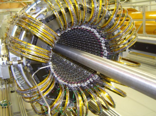
Photographs of the ATLAS pixel detector fully assembled. (a) Pixel barrel layer-2, (b) one stack of disks.
III.6 Summary on Hybrid Pixel Detectors
Hybrid pixel detectors constitute the state of the art in pixel detectors at present. The have proven to be suited for LHC conditions in terms of readout speed as well as radiation hardness. Every cell already provides complex signal processing including zero suppression. Hits are temporarily stored during the trigger latency of several . The 3D capability renders pixel detectors at LHC superior to any other detector regarding pattern recognition capability. The spatial hit resolution is about 10-15 in the transverse direction.
As disadvantages one would probably have to consider the comparatively large material budget of 2.5 in ATLAS and CMS and 1 in ALICE, mostly due to cooling, support structure and services. The module production is quite laborious including many production steps such as bump bonding and flip-chipping, which are also a cost issue.
IV Pixel R&D for Future Colliders
IV.1 Challenges imposed by a Super-LHC
The data rate and also the radiation levels expected at an LHC upgrade, called Super-LHC or sLHC, are a factor of up to ten higher than at the LHC, i.e. about 21016neq/cm2 at a radius of 4 cm. Concerning irradiatio issues there are mainly three effects as a consequence (see review moll2006 ).
-
1.
A change of the effective doping concentration (higher depletion voltage necessary, under-depletion)
-
2.
An increase of leakage current (increase of shot noise, thermal runaway)
-
3.
An increase of charge carrier trapping (loss of charge)
Several routes to cope with this are being pursued, among them the development of even more radiation hard silicon based on oxygenated float-zone (DOFZ), Czochralski (Cz), n+ in p silicon sensors, as well as epitaxial silicon moll2006 . For this lecture I would like to address in this context two new approaches which are more linked to pixel detectors: diamond pixel detectors and 3D-silicon devices.
IV.2 Diamond Pixels
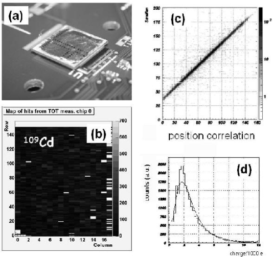
CVD-Diamond as a sensor material has been developed by the CERN RD group RD42 for many years RD42 . Charge collection distances approaching 300 m has also triggered the development of a hybrid pixel detector using diamond as sensors diamond-pixels ; kagan_PIX2005 . The non-uniform field distribution inside CVD-diamond, which originates from the grain structure in the charge collecting bulk (cf. Fig. 32(a)) introduces polarization fields inside the sensor due to charge trapping at the grain boundaries which superimpose on the biasing electric field. This results in position dependent systematic shifts in the track reconstruction with a typical average grain size of 100m - 150m lari04 . Diamond sensors with charge collection distances in excess of 300m have been fabricated and tested Kagan_Hiroshima . Single chip pixel modules as well as a full size wafer scale 16-chip module assembled using ATLAS front-end chips have been built and tested. Figure 31(a) and (b) show the diamond pixel detector and a hit response pattern obtained by exposing the detector to a 109Cd source of 22 keV rays, which deposits approximately 1/4 of the charge of a minimum ionizing particle. The single chip module has been tested in a high energy (180 GeV) pion beam at CERN, the module in a 4 GeV electron beam at DESY. Figure 31(c) and (d) show position correlation and the charge distribution of the diamond pixel detector in a high energy beam, respectively. A spatial resolution of = 12m has been measured with the single chip module at high energies with 50m pixel pitch. A technical challenge to produce a wafer scale module lies in the hybridization process, i.e. bump deposition and flip-chipping. Figure 32 shows the 16-chip diamond module (Fig. 32(b), chips are on the bottom) and its tuned threshold map (Fig. 32(c)) with a very small dispersion of only 25e- and good bump yield homogeneity. One chip was damaged during test beam by electrostatic discharge. The rms of the position residuals was measured to 24 m in the DESY 6 GeV beam kagan_PIX2005 including a large multiple scattering contribution from the beam telescope.
IV.3 3D silicon sensors
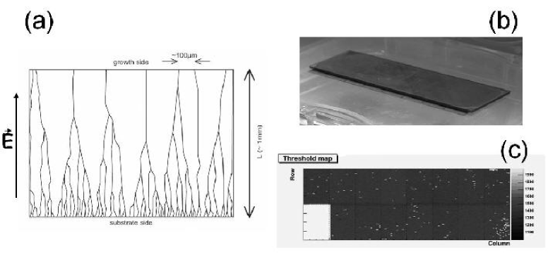
So-called 3D silicon detectors have been developed 3D-parker to overcome several limitations of conventional planar Si-pixel detectors, in particular in high radiation environments, in applications with inhomogeneous irradiation and in applications which require a large active/inactive area ratio such as protein crystallography.
A 3D-Si-structure (Fig. 33(a)) is obtained by processing the n+ and p+ poly silicon electrodes into the detector bulk rather than by conventional implantation on the surface. This is done by combining VLSI and MEMS (Micro Electro Mechanical Systems) technologies. Charge carriers drift inside the bulk parallel to the detector surface over a short drift distance of typically 50m. Another feature is the fact that the edge of the sensor can be a collection electrode itself thus extending the active area of the sensor to within few m to the edge. Edge electrodes also avoid inhomogeneous fields and surface leakage currents which usually occur due to chips and cracks at the sensor edges. The main advantages of 3D-silicon detectors, however, come from a different way of charge collection (cf. Fig. 33(b)) and the fact that the electrode distance is short (50m) in comparison to conventional planar devices at the same total charge. This results in a fast (1-2 ns) collection time, low ( 10V) depletion voltage and, with edge electrodes in addition, a large active/inactive area ratio of the device. The technical fabrication is much more involved than for planar processes and requires a bonded support wafer and reactive ion etching of the electrodes into the bulk. Prototype detectors using strip or pixel electronics have been fabricated parker_pix2005 and show encouraging results with respect to speed (3.5 ns rise time) and radiation hardness ( 1015 protons/cm2) 3DPortland . 3D-pixel detectors with ATLAS frontend electronics have also been successfully built. Preliminary results have been presented in cinzia2006 .
IV.4 Monolithic and Semi-Monolithic Pixel Detectors
Monolithic pixel detectors, in which amplifying and logic circuitry as well as the radiation detecting sensor are one entity, are in the focus of present developments for future experiments. To reach this ambitious goal, optimally using a commercially available and cost effective technology, would be another breakthrough in the field. The present developments have been much influenced by RD for vertex tracking detectors at future colliders such as the International Linear Collider (ILC) TESLA-TDR . Very low (1 X0) material per detector layer, small pixel sizes (20mm) and a high rate capability (80 hits/mm2/ms) are required, due to the very intense beamstrahlung of narrowly focussed electron beams close to the interaction region, which produce electron positron pairs in vast numbers. High readout speeds with typical line rates of several MHz and a 40s frame readout time are necessary. At present, two developments have already reached some level of maturity: so called CMOS active pixels and DEPFET pixels.
IV.4.1 CMOS active pixels
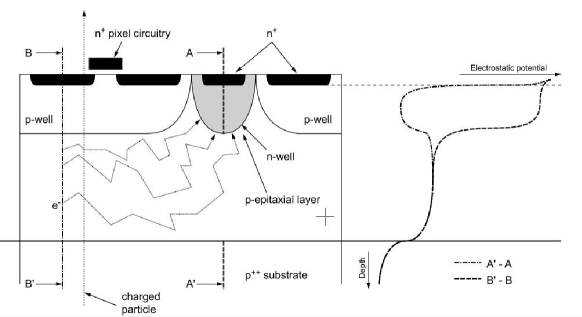
In some CMOS chip technologies a lightly doped epitaxial silicon layer of a few to 15m thickness between the low resistivity silicon bulk and the planar processing layer can be used for charge collection meynants98 ; MAPS1 ; MAPS2 . The generated charge is kept in a thin epi-layer atop the low resistivity silicon bulk by potential wells that develop at the boundary and reaches an n-well collection diode by thermal diffusion (cf. Fig. 34). With small pixel cells collection times in the order of 100 ns are obtained. The charge collecting epi-layer is – technology dependent – at most 15m thick and can also be completely absent. The attractiveness of active CMOS pixels lies in the fact that standard CMOS processing techniques are employed and hence they are potentially very cheap.
CMOS active pixel sensor development are pursued by many groups which partially collaborate in various projects (BELLE-upgrade, STAR-upgrade, ILC, CBM at GSI) who use similar approaches to develop large scale CMOS active pixels, also called MAPS (Monolithic Active Pixel Sensors) MAPS1 . The sensor is depleted only directly under the n-well diode. The signal charge is hence very small (1000e) and full charge collection is obtained only in the depleted region under the n-well electrode. Low noise electronics is therefore the challenge in this development.
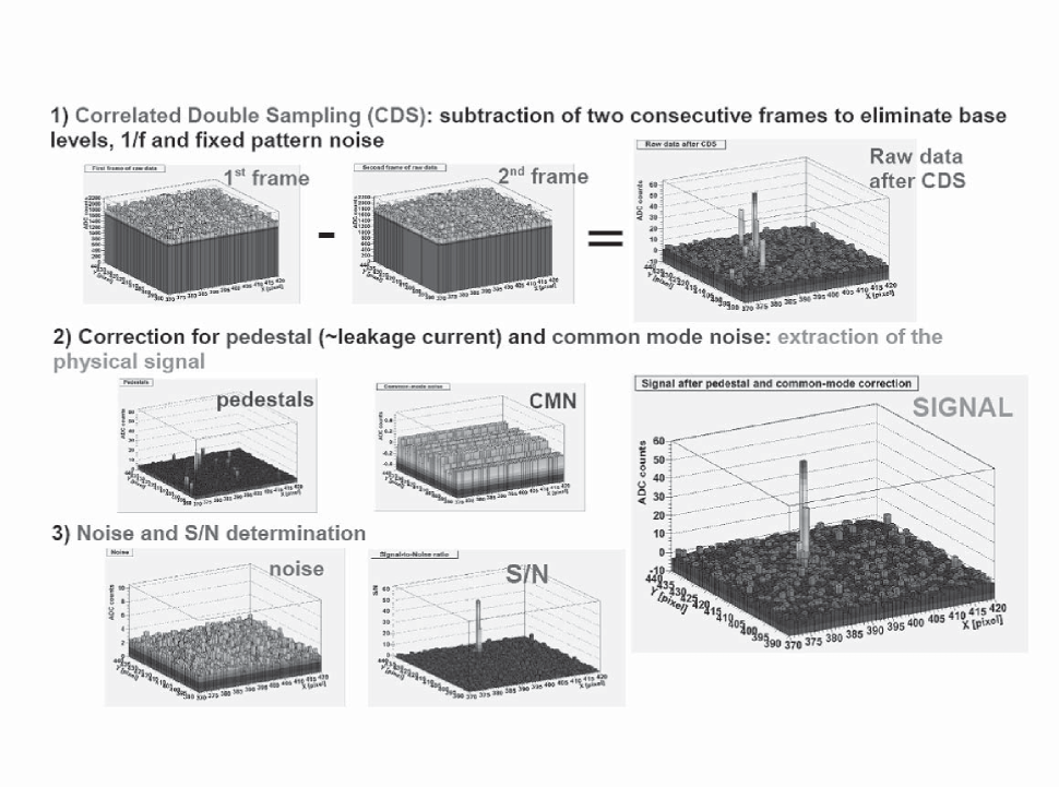
Matrix readout of MAPS is performed using a standard 3-transistor circuit (line select, source-follower stage, reset) commonly employed by CMOS matrix devices, but can also include current amplification and current memory Dulinski03 . In the active area only nMOS transistors are permitted because of the n-well/p-epi collecting diode which does not permit other n-wells. For an image two complete frames are subtracted from each other (correlated double sampling, CDS) to eliminate base levels, 1/f and fixed pattern noise (see Figure 35). In a second step pedestals and common mode noise are subtracted to extract the signal and to determine the remaining noise. Detector sizes up to 19.417.4 mm2 with 1M pixels have been tested. Frame speeds of 10s for 132x48 pixels have been reached for the BELLE development, with a noise figure of 30-50e- varner_pix2005 . With other pixel matrices with slower readout noise values of 15-20 e-, S/N ratios larger than 20 and spatial resolutions of 1.5m (5m) for 20m (40m) pitch have been measured winter_PIX2005 . The presently favored technology is the AMS 0.35m OPTO process, which possesses a 10m thick epitaxial layer. Regarding radiation hardness MAPS appear to sustain non-ionizing radiation (NIEL) to 1012neq. The effects of ionizing radiation damage (IEL), the main damage source at the ILC, are threshold shifts and leakage currents in and between nMOS transistors. The damage effects are less severe when short readout integration times (10s) are used. This way doses of about 10 kGy can be tolerated winter_PIX2005 .
The present focus of further development lies in improving the radiation tolerant design, making 50m thin detectors, making larger area devices for instance by stitching over reticle boundaries MAPS2 , and increasing the charge collection performance in the epi-layer.
IV.4.2 DEPFET pixels
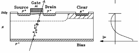
In so-called DEPFET pixel sensors kemmer87 a FET transistor is implanted in every pixel on a sidewards depleted gatti84 bulk. Electrons generated by radiation in the bulk are collected in a potential minimum underneath (m) the transistor channel (internal gate) thus modulating its current (Fig. 36). Electrons collected in the internal gate are completely sandow-kreuth05 removed by a clear pulse applied to a dedicated contact outside the transistor. Amplification values of 300 pA per collected electron in the internal gate have been achieved. Further current amplification and storage enters at the second level stage. The bulk is fully depleted yielding large signals and the small capacitance of the internal gate offers low noise operation, for a very large S/N ratio. This in turn can be used to fabricate very thin devices. Thinning of pn-diodes to a thickness of 50m using a technology based on wafer bonding and deep anisotropic etching has been successfully demonstrated laci04 .
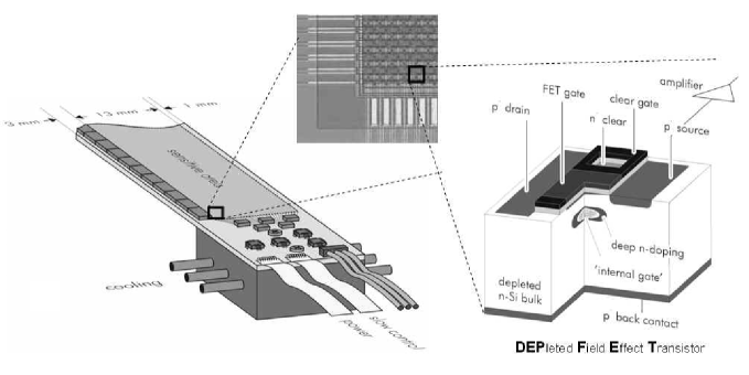
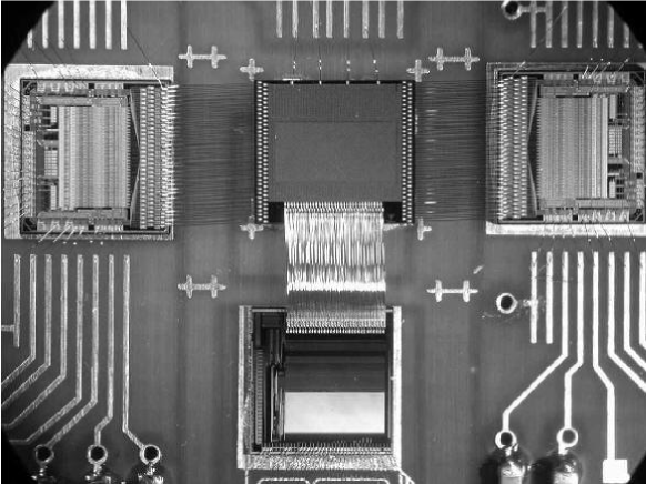
Readout of a DEPFET matrix is done by selecting a row by a gate voltage from a sequencer chip (SWITCHER) to the external gate. The drains are connected column-wise delivering their current to a current-based readout chip (CURO) with amplification and current storage at the bottom of the column Trimpl02 ; DEPFET_Portland . A sketch of a module made of DEPFET sensors is shown in Fig. 37(top). Figure 37(bottom) shows a DEPFET pixel matrix readout system used in the test beam.
The radiation tolerance, in particular against ionizing radiation, which is expected to doses of 2 kGy due to beamstrahlung at the ILC, again is a crucial question. Irradiation with 30 keV X-rays up to doses of 10 kGy, about five times the amount expected at the ILC, have lead to transistor threshold shifts of only about 4 V. Threshold shifts of this order can be coped with by an adjustment of the corresponding gate voltages supplied by the SWITCHER chip. The estimated power consumption for a five layer DEPFET pixel vertex detector at the ILC – assuming a power duty cycle of 1:200 – is in the order of 5-10W. Such a performance renders a very low mass detector without cooling pipes feasible. A DEPFET pixel matrix with 12864 pixels has been tested in a 6 GeV electron beam at DESY wermes_LECC2005 . The noise values obtained for the full system in the test beam including sampling noise of the CURO chip is 200-300e-. The signal in a 450 thick DEPFET sensor was about 35000e-. At 6 GeV beam energy the spatial residuals are still multiple scattering dominated. Residuals on the order of 10m are obtained, while with the large S/N value of 144 true space resolutions in the order of 2m should be possible and has been recently demonstrated using high energy test beams at CERN jaap_private .
Acknowledgments
I would like to thank the directors and organizers of the 2006 SLAC Summer Institute for their effort and efficiency in organizing this highly motivating and interesting research school.
References
- [1] G. Charpak. Particle detection by gas discharges. J. Phys., 30:c2–c86, 1969.
- [2] G. Charpak. Development of multiwire proportional chambers. CERN Courier, 6:174–176, 1969.
- [3] J.P. Alexander et al. Prototype Results of a High Resolution Vertex Drift Chamber For The Mark-II SLC Upgrade Detector. Nucl. Inst. and Meth., A252:350–356, 1986.
- [4] J.B.A. England, B.D. Hyams, L. Hubbeling, Joseph C. Vermeulen, and P. Weilhammer. A silicon strip detector with 12m resolution. Nucl. Inst. and Meth., 196:149–151, 1986.
- [5] L. Rossi, P. Fischer, T. Rohe, and N. Wermes. Pixel Detectors: From Fundamentals to Applications. Springer, Berlin, Heidelberg, 2006.
- [6] P. Kuijer et al. Inner tracking system of the ALICE experiment. Nucl. Inst. and Meth., A530:28–32, 2004.
- [7] S. Ramo. J. Appl. Phys., 9:635, 1938.
- [8] E. Durand. Electrostatique, Tome II. Masson et Cie, Paris, 1966.
- [9] I. Gorelev et al. A measurement of Lorentz angle and spatial resolution of radiation hard silicon pixel sensors. Nucl. Inst. and Meth., A481:204–221, 2002.
- [10] A. Dorokhov et al. Tests of silicon sensors for the CMS pixel detector. Nucl. Inst. and Meth., A530:71–76, 2004.
- [11] O. Ehrmann, G. Engelmann, J. Simon, and H. Reichl. A bumping technology for reduced pitch. In Proc. Second International TAB Symposium, pages 41–48, San Jose, USA, 1990.
- [12] A.M. Fiorello. ATLAS bump bonding process. In Pixel 2000 Conference, Genoa, Italy, June 2000.
- [13] J. Wolf, G. Chmiel, and H. Reichl. Lead/Tin (95/5 ) solder bumps for flip chip applications based on Ti:W(N)/Au/Cu underbump metallization. In Proc. 5th Intl. TAB/Advanced Packaging Symposium ITAP, pages 141–152, San Jose, USA, 1993.
- [14] R. Wunstorf. Systematische Untersuchungen zur Strahlenresistenz von Silizium-Detektoren für die Verwendung in Hochenergiephysik-Experimenten. PhD thesis, Universität Hamburg, Germany, 1992.
- [15] G. Lindström ond others. Radiation hard silicon detectors – developments by the RD48 (ROSE) collaboration. Nucl. Inst. and Meth., A 466:308–326, 2001.
- [16] M. Moll. Radiation tolerant semiconductor sensors for tracking detectors. Nucl. Inst. and Meth., A565:202–211, 2006.
- [17] M. Moll, E. Fretwurst, M. Kuhnke, and G. Lindström. Relation between microscopic defects and macroscopic changes in silicon detector properties after hadron irradiation. Nucl. Inst. and Meth., B186:100–110, 2002.
- [18] V. Eremin, E. Verbitskaya, and Z. Li. Effect of Radiation induced deep Level Traps on Si Detector Performance. Nucl. Inst. and Meth., A476:537–549, 2002.
- [19] M. Moll, E. Fretwurst, and G. Lindström. Leakage current of hadron irradiated silicon detectors – material dependance. Nucl. Inst. and Meth., A426:87–93, 1999.
- [20] R. H. Richter et al. Strip detector design for ATLAS and HERA-B using two-dimensional device simulation. Nucl. Inst. and Meth., A 377:412–421, 1996.
- [21] T. Rohe et al. Fluence dependence of charge collection of irradiated pixel sensors. Nucl. Inst. and Meth., A552:232–238, 2005.
- [22] G. Alimonti ond others. Analysis of the production of ATLAS indium bonded pixel modules. Nucl. Inst. and Meth., A 565:296–302, 2006.
- [23] L. Blanquart et al. FE-I1: A Front-end Readout Chip Designed in a Commercial 0.25m process for the ATLAS pixel detector at LHC. IEEE Trans. Nucl. Sci., vol. 51, no. 4:1358–1364, 2004.
- [24] L. Blanquart et al. Analog front-end cell designed in a commercial 0.25m process for the ATLAS pixel detector at LHC. Nucl. Inst. and Meth., A456:217–231, 2001.
- [25] W. Erdmann. The 0.25 ìm front-end for the cms pixel detector. In 12th Intl. Workshop on Vertex Detectors, Low Wood, Lake Windermere, Sept. 2003.
- [26] R. Baur et al. Readout architecture of the CMS pixel detector. Nucl. Inst. and Meth., A465:159–165, 2000.
- [27] H.C. Kastli, M. Barbero, W. Erdmann, Ch. Hormann, R. Horisberger, D. Kotlinski, and B. Meier. Design and performance of the cms pixel detector readout chip. Nucl. Inst. and Meth., A565:188–194, 2006.
- [28] G. Pepato ond others. The mechanics and cooling system of the ALICE silicon pixel detector. Nucl. Inst. and Meth., A 565:6–12, 2006.
- [29] W. Adam et al. Development of Diamond Tracking Detectors for High Luminosity Experiments at the LHC. Nucl. Inst. and Meth., A447:244, 2000.
- [30] M. Keil et al. New results on diamond pixel sensors using ATLAS frontend electronics. Nucl. Inst. and Meth., A511:153–159, 2003.
- [31] H. Kagan et al. Radiation hard diamond sensors for future tracking applications. Nucl. Inst. and Meth., A565:278–283, 2006.
- [32] T. Lari, A. Oh, N. Wermes, H. Kagan, M. Keil, and W. Trischuk. Characterization and modelling of non-uniform charge collection in CVD diamond pixel detectors. Nucl. Inst. and Meth., A537:581–593, 2005.
- [33] H. Kagan et al. Recent Advances in Diamond Detector Development. Nucl. Inst. and Meth., A541:221–227, 2005.
- [34] C. Kenney, S. Parker, J. Segal, and C. Storment. Silicon detectors with 3-D electrode arrays: fabrication and initial test results. IEEE Trans. Nucl. Sci., vol.48, no.4:1224–1236, 1999.
- [35] C.J. Kenney, J.D. Segal, E. Westbrook, S. Parker, J. Hasi, C. Da Via, S. Watts, and J. Morse. Radiation hard diamond sensors for future tracking applications. Nucl. Inst. and Meth., A565:272–277, 2006.
- [36] S.I. Parker et al. Measurements of fast rise-time pulses from 3D silicon sensors. In presented at IEEE Nuclear Science Symposium, Portland, USA, Oct. 2003.
- [37] C. da Via’. Recent results on 3d silicon sensors. In 6th Int. Symposium on Development and Application of Semiconductor Tracking Detectors, Carmel, USA, September 2006.
- [38] T. Behnke, S. Bertolucci, R.-D. Heuer, and R. Settles (eds.). TESLA Technical Design Report. Report DESY-01-011, Vol. IV, 2001.
- [39] R. Turchetta, J.D. Berst, B. Casadei, G. Claus, C. Colledani, W. Dulinski, Y. Hu, D. Husson, J.-P. Le-Normand, J.L. Riester, G. Deptuch, U. Goerlach, S. Higueret, and M. Winter. A monolithic active pixel sensor for charged particle tracking and imaging using standard VLSI CMOS technology. Nucl. Inst. and Meth., A458:677–689, 2001.
- [40] G. Meynants, B. Dierickx, and D. Scheffer. CMOS active pixel image sensor with CCD performance. Proceedings SPIE - Int. Soc., Opt. Eng. (USA), 3410:68–76, 9., 1998.
- [41] A. Gay et al. High Resolution CMOS Sensors for a Vertex Detector at the Linear Collider. Nucl. Inst. and Meth., A549:99–102, 2005.
- [42] W. Dulinski, D. Berst, F. Cannillo, G. Claus, C. Colledani, et al. CMOS monolithic active pixel sensors for high resolution particle tracking and ionizing radiation imaging. In Proc. Frontier Detectors for Frontier Physics 2003, Elba, May 2003.
- [43] G. Varner et al. Development of the Continuous Acquisition Pixel (CAP) sensor for high luminosity lepton colliders. Nucl. Inst. and Meth., A565:126–131, 2006.
- [44] M. Winter. Adapting CMOS sensors to future vertex detectors. In PIXEL 2005 Intl. Workshop, Bonn, Sept 2005.
- [45] J. Kemmer and G. Lutz. New Semiconductor Detector Concepts. Nucl. Inst. and Meth., A253:356–377, 1987.
- [46] E. Gatti and P. Rehak. Semiconductor drift chamber - an application of a novel charge transport scheme. Nucl. Inst. and Meth., A225:608, 1984.
- [47] C. Sandow et al. CLEAR Performance of Linear DEPFET Structures. In 10th European Symposium on Semiconductor Detectors, Wildbad-Kreuth, Germany, June 2005. submitted to Nucl. Instr. Meth.
- [48] L. Andricek, G. Lutz, M. Reiche, and R.H. Richter. Processing of ultra thin silicon sensors for future linear collider experiments. IEEE Trans. Nucl. Sci., vol.51, no.3:1117–1120, 2004.
- [49] M. Trimpl, L. Andricek, P. Fischer, G. Lutz, R.H. Richter, L. Strüder, J. Ulrici, N. Wermes, and M. Trimpl. A fast readout using switched current techniques for a DEPFET-pixel vertex detector at tesla. Nucl. Inst. and Meth., A511:257–264, 2003.
- [50] N. Wermes et al. New results on DEPFET pixel detectors for radiation imaging and high energy particle detection. In IEEE Trans. Nucl. Sci., Portland, USA, Oct. 2003. accepted by IEEE Trans. Nucl. Sci (2004).
- [51] N. Wermes. Pixel detectors. In Electronics for LHC and futire experiments, LECC-2005, Heidelberg, Oct. 2005.
- [52] J. Velthuis (Bonn Univ.). Private communication.