Universal behavior of the electron g-factor in GaAs/AlGaAs quantum wells
Abstract
The Zeeman splitting and the underlying value of the -factor for conduction band electrons in GaAs/AlxGa1-xAs quantum wells have been measured by spin-beat spectroscopy based on a time-resolved Kerr rotation technique. The experimental data are in good agreement with theoretical predictions. The model accurately accounts for the large electron energies above the GaAs conduction band bottom, resulting from the strong quantum confinement. In the tracked range of optical transition energies from 1.52 to 2.0 eV, the electron -factor along the growth axis follows closely the universal dependence (with measured in eV); and this universality also embraces AlxGa1-xAs alloys. The in-plane -factor component deviates notably from the universal curve, with the degree of deviation controlled by the structural anisotropy.
pacs:
78.47.+p, 75.75.+a, 73.21.FgI Introduction
The Lande or -factor of carriers in a solid is one of the fundamental properties of this material Abragham ; Awsch ; Kosaka . For conduction band electrons in semiconductors and semiconductor heterostructures it may deviate strongly from the free electron -factor in vacuum due to the spin-orbit interaction, e. g. it is -0.44 in GaAs, -1.64 in CdTe and can be as large as -51 in the narrow band gap semiconductor InSb Landolt .
Invention of spintronics has increased the interest in spin manipulation in semiconductor heterostructures Awsch ; Zut04 and therefore in control of the carrier -factors. GaAs/AlxGa1-xAs heterostructures are very suitable for this purpose as with increasing carrier confinement the electron -factor’s absolute value decreases and even crosses zero. Therefore, the Zeeman splitting can be fully suppressed by a proper choice of structure design parameters and/or external conditions like strain, temperature, electric field, and orientation of the structure in external magnetic field Salis01 ; Jiang01 ; Oestreich95 .
The electron -factor in GaAs/AlxGa1-x quantum well (QW) structures has been measured by various experimental techniques such as spin-flip Raman scattering Sapega92 , optical orientation Snelling91 ; Ivchenko92_hmfsp ; Kalevich92_zhetf ; Kalevich95_ftt , optically detected magnetic resonance Baranov93 ; vanKesteren , spin quantum beats in emission Heberle94 ; Hannak95 ; Amand97 ; LeJeune97 , in absorption Bar-Ad92 , or in Kerr rotation Malinowski00_sss ; Malinowski00_prb . However, most of these studies have been limited to certain widths of the quantum wells and only in a few papers the well width dependence of the -factor has been reported Snelling91 ; Malinowski00_prb ; Hannak95 ; LeJeune97 .
The first concise analysis of the electron g factor in QWs was performed in the framework of the Kane model Ivchenko92_ftp , followed by more detailed considerations Ivchenko97_ssc ; Kiselev_PRB98 ; Kiselev_PhysStatSol99 ; Ivch04 . The model calculations predict a strong variation of the -factor value, including a sign reversal in the GaAs/AlxGa1-x heterosystem, and of its anisotropy with well width. Both quantities are controlled by the strength of electron confinement in the QWs determined mostly by the well width and barrier height. These theoretical predictions were further substantiated by experimental data Sirenko ; Kiselev_JCrystGrowth98 ; Malinowski00_prb ; LeJeune97 . The published results are commonly presented as a dependence of the -factor value on the QW width, i.e. a set of different dependencies corresponding to different barrier heights (controlled by the Al content) is required to cover the whole range of possible QW structures. In CdTe/Cd1-xMgxTe heterostructures, whose band structure is similar to that of GaAs/AlxGa1-x structures, to a good approximation a universal dependence of the electron -factor on the heterostructure band gap (i.e., on the energy of the optical transition between the ground states of confined electrons () and holes ()) has been reported Sir97 : the -factor was sensitive mostly to the value of the band gap itself, but not to the way how this gap has been obtained by the structure’s design parameters.
The goal of this paper is to check experimentally and theoretically, whether this universality can be extended to GaAs/AlxGa1-x heterosystems, and if yes, what the origins of this universality are. We present experimental results for the time-resolved pump-probe Kerr rotation, which allow us to determine the transverse component of the electron -factor with high accuracy from the frequency of the spin precession in an external magnetic field. Model calculations accounting for the interaction between lowest conduction band and the upper valence bands have been performed for the longitudinal and transverse components of the electron -factor in structures with the Al content varied from 0 to 0.45. We found that for the longitudinal component a universal dependence is strongly supported. At the same time, the transverse component deviates notably from a universal curve, with the degree of deviation controlled by the structural anisotropy.
II Experimental details
The GaAs/AlxGa1-x heterostructures have been grown by molecular-beam epitaxy on (100) oriented GaAs substrates. The sample parameters are collected in Table 1. Samples and consist of several single QWs of different width separated by 50 nm thick AlxGa1-xAs barriers to prevent electronic coupling between the wells. Samples , and contain only one QW. All structures are nominally undoped, but due to residual doping of the barriers presence of background electrons in the QWs has been established from the observation of emission of negatively charged excitons. The background electrons density does not exceed cm-2.
For optical measurements the samples were immersed in pumped liquid helium at a temperature of 1.6 K, and magnetic fields up to 7 T were applied perpendicular to the structure growth axis (Voigt geometry). The structures were characterized by means of photoluminescence (PL) excited by 532 nm laser light with an excitation density below 0.3 W/cm2.
| Sample, Al content | QW width (nm) | transition | Laser energy (eV) | |
| (p343), x=0.33 | 14.3 | 1.530 | 0.34 0.01 | |
| 10.2 | 1.543 | 0.27 0.01 | ||
| 7.3 | 1.569 | 0.13 0.01 | ||
| 4.2 | 1.622 | 0.06 0.004 | ||
| (p340), x=0.34 | 17.2 | 1.527 | 0.40 0.01 | |
| 13 | 1.535 | 0.33 0.01 | ||
| 13 | 1.542 | 0.33 0.01 | ||
| 13 | 1.597 | 0.32 0.01 | ||
| 8.8 | 1.555 | 0.20 0.005 | ||
| 5.1 | 1.600 | 0.00 0.04 | ||
| (p337), x=0.28 | 10 | 1.544 | 0.26 0.005 | |
| (11302), x=0.25 | 8.4 | 1.559 | 0.17 0.01 | |
| GaAs buffer | 1.559 | 0.43 0.005 | ||
| (e294), x=0.32 | 8.8 | 1.555 | 0.21 0.01 | |
| GaAs buffer | 1.515 | 0.44 0.001 | ||
| GaAs buffer | 1.529 | 0.44 0.001 | ||
| GaAs buffer | 1.543 | 0.43 0.006 | ||
| GaAs buffer | 1.553 | 0.42 0.004 |
The electron -factor was evaluated from the frequency of the electron spin quantum beats corresponding to the Larmor precession frequency in magnetic field. A pump-probe technique with polarization sensitivity based on time-resolved Kerr rotation was used for detection of the spin beats (see e. g. Refs. Awsch, ; Crooker97, ). A Ti:Sapphire laser emitting 1.8 ps pulses at a repetition rate of 75.6 MHz was tuned in resonance with the QW exciton transition. The pump beam was circularly polarized by means of an elasto-optical modulator operating at 50 kHz. The excitation density was kept as low as possible in the range from 0.2 to 1 W/cm2. The probe beam was linearly polarized, its intensity was about 20 of the pump beam. The rotation angle of the linearly polarized probe pulse reflected from the sample due to the Kerr rotation, was detected by a balanced diode detector and a lock-in amplifier. The time-resolved Kerr rotation signal as function of the delay between probe and pump pulses gives the evolution of the electron spin coherence generated by the pump.
III Experimental results
A typical photoluminescence spectrum obtained for sample containing four single QWs of different thickness is shown in Fig. 1. The emission from the GaAs buffer layer is presented by the dashed line. The luminescence from the QWs is dominated by recombination of excitons, whose energy increases for the narrow QWs due to confinement. The low energy shoulders of the excitonic lines are due to the negatively charged excitons (trions) recombination Buhmann95 . Trions consisting of two electrons and a hole are formed by a background electron and a photogenerated exciton.

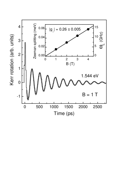
An example of time-resolved spin quantum beats in a 10 nm wide QW detected in a magnetic field of T is shown in Fig. 2. The experimental data are plotted by the black line. The excitation energy of 1.544 eV is resonant with the exciton transition. The periodic oscillations of the Kerr signal are due to the precession of coherently excited electron spins about the magnetic field, with the oscillation period given by the spin splitting in the conduction band . Therefore, the Larmor precession frequency allows precise determination of the transverse component of the electron -factor by
| (1) |
where is the Bohr magneton. Note that the sign of the -factor cannot be determined, but only its absolute value. For that purpose, we fit the spin-beat dynamics by form for an exponentially damped oscillation. In case of a single frequency and a single decay time, which gives an appropriate description for most of the studied structures, this form is given by the following equation:
| (2) |
with an amplitude . is the decay time of spin coherence, which for an electron spin ensemble corresponds to the spin dephasing time Awsch ; Zhu06 . An example for the result of a fitting to the experiment is given in Fig. 2 by the thick grey line. Here we exclude from the analysis the initial 15-30 ps after the pump pulse, which are contributed by the fast relaxation of holes Linder98 ; Amand97 ; Gerlovin04 .
In the inset, the determined Zeeman splitting is plotted as a function of magnetic field. The corresponding values of the Larmor frequency are also given on the right vertical axis. The slope of the B-linear dependence gives . The decay time of the spin beats in Fig. 2 is 880 ps and is considerably longer than the radiative decay of resonantly excited excitons which does not exceed 100 ps in GaAs/AlxGa1-xAs QWs Deveaud . Therefore, we conclude that the detected spin beats are provided by background electrons whose spin coherence is photogenerated by the trion formation Zhu06 .
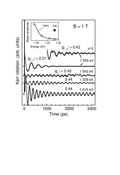
Not in all cases the Kerr signals can be described by a single frequency and/or single decay time. Figure 3 illustrates a more complicated case observed in sample for a 8.8 nm wide QW. The excitation energy of 1.515 eV is resonant with the exciton transition of the GaAs buffer layer and the observed oscillations with are in accord with the known -factor value of bulk GaAs (GaAs) Landolt . The decay of the spin beats shows two characteristic times. The fast one of 360 ps may be associated with the exciton lifetime and the long one, which exceeds 3 ns describes the dephasing of the background electrons in the buffer layer Kikkawa98 . The resonant excitation into the exciton states of GaAs results in the largest amplitude of the Kerr signal. However, pronounced spin beats can be observed when the excitation energy is detuned from the resonance condition and shifted further up by 27 meV to the energy of 1.543 eV, which is still below any QW resonance. The Kerr signal at these energies is provided by the exciton-polariton reflection spectrum Tredicucci , which is governed by the quantization of polaritons in the GaAs buffer layer. The spin beats period is independent of the excitation energy, as it is determined by spin oriented carriers, which relax from the excited states to the bottom of the conduction band and precess there with . The amplitude of the Kerr signal, however, decreases, as shown by the open circles in the inset.
An increase of the laser energy to 1.553 eV brings it in resonance with the QW exciton. The beats period increases about twice corresponding to . The spin beats are damped with a decay time ps. At longer delays exceeding 1000 ps the oscillation picture becomes irregular, suggesting that at least two periodic processes overlap. The signal was fitted by an equation accounting for two frequencies with different decay times:
| (3) |
As one can see from the fit in Fig. 3 shown by the grey lines, the experiment at longer delays can be described by spin beats of QW electrons with superimposed with beats. The latter beats can be attributed to electrons precessing in the GaAs buffer. The relative intensities of the amplitudes and are given in the inset of Fig. 3.
To obtain further insight, a 13 nm wide QW in sample has been excited resonantly with three optical transitions corresponding to the ground state of the heavy-hole exciton (), of the light-hole exciton () and of the exciton related to the second confined electron and levels (). For all cases spin beats with almost the same period corresponding to have been found (see Table 1). As the value of the electron - factor should strongly depend on the electron energy, we therefore conclude that the Kerr signal is provided by electrons which relax to the bottom of the conduction band shortly after the photogeneration and precess there. It is remarkable that the electron precession can be accessed through the optical transition.

After having given some insight into the general features of the experimental data and their analysis, we turn to the problem of the -factor dependence on the carrier confinement conditions. Time-resolved Kerr rotation signals detected for the laser energy resonant with the exciton optical transitions in QWs of different width are given in Fig. 4. One can see that the spin beats frequency, which is proportional to of the conduction band electrons, decreases with decreasing well width. Oscillations cannot be resolved in a 5.1 nm QW with the exciton energy at 1.600 eV. A further decrease of the QW width down to 4.2 nm restores the spin beat oscillations. The determined values are given in the figure and are collected also in Table 1.
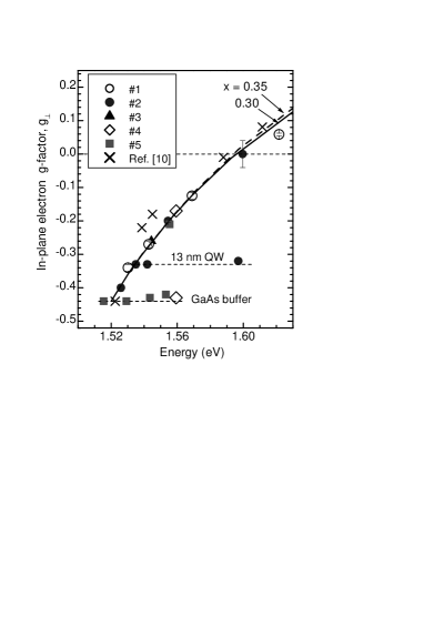
The experimental values for are plotted in Fig. 5 as function of excitation energy. Most of the data, except for some results for a 13 nm QW and the GaAs buffer which were measured for non-resonant excitation, were detected when the laser was resonant with the exciton state . Measurements on different structures confirm the monotonic decrease of the -factor absolute value with increasing energy leading to a sign reversal at 1.600 eV. Our results are in good agreement with the data of Snelling et al. Snelling91 obtained by the optical orientation technique. They are also in good agreement with model calculations for Al contents of and 0.35 shown by the solid and the dashed lines, respectively. Details of these calculations are given below in Sec. IV. We note that the calculated dependencies are plotted as function of energy of the optical transition between the confined carrier levels and without accounting for the exciton binding energy. The latter may shift these curves to lower energy by about 8 meV in wide QWs of about 20 nm and by about 13 meV in 4 nm QWs Bimberg .
IV Calculation of the electronic -factor and comparison with experiment.
Here we present results of model calculations for the longitudinal and transverse components of the electronic -factor in GaAs/AlxGa1-xAs QWs for a wide range of well widths from 1 to 30 nm and Al contents , which control the barrier height. In Fig. 6 the calculated -factors are shown as function of the e1-hh1 optical transition energy. This provides a convenient comparison with experiment, as the -factor is addressed in dependence of an easily measurable quantity.
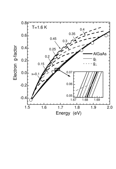
To prepare Fig. 6, it was necessary, first, to calculate accurately the lowest quantized states of electrons and heavy holes for each set of heterostructure parameters, and, second, to evaluate the -factor tensor for the calculated electron state. To achieve advanced accuracy in the energy levels, we applied the Kane multiband Hamiltonian, accounting exactly for the coupling between the lowest conduction band and the upper valence bands and , and retaining also all remote band terms that notably affect the dispersion of the relevant quasi-particles in conduction and valence band. Details of the computational procedure were presented elsewhere Kiselev_PRB01 ; Kiselev_APL02 . Then by directly following the prescriptions in Ref. Kiselev_PhysStatSol99, , two independent components of the -factor tensor at the bottom of the first electron subband in the QW structure can be explicitly calculated: the in-plane -factor using Eq. (6) in Ref. Kiselev_PhysStatSol99, and the -factor along the growth direction with help of Eq. (10) in Ref. Kiselev_PhysStatSol99, .
| GaAs | Al0.35Ga0.65As | Interpolation | |
|---|---|---|---|
| (eV) | 0.341 | 0.32 | basic, linear |
| (eV) | 28.9 | 26.7 | basic, linear for |
| 0.067 | 0.09 | composite | |
| -0.44 | 0.58 | composite | |
| 0.45 | 0.45 | constant |
The parameters characterizing the band structure of the AlxGa1-xAs alloy are known to a great definiteness. Numeric values for all applicable quantities are collected in Table 2 for GaAs and Al0.35Ga0.65As (the data are taken from Ref. Landolt, ). The following scheme for parameter evaluation has been adopted for an arbitrary Al composition : for most of the parameters (named basic in Table 2), we use a simple linear interpolation (extrapolation for ). This group contains the interband momentum matrix element and the spin-orbit splitting in the valence band. Rigorously speaking, higher accuracy can probably be achieved if also the bowing constants for the interpolation curves were known, but for the studied range linear interpolations should be sufficient. As the only notable exception, we use the common interpolation equation with bowing term for the AlxGa1-xAs band gap Landolt :
| (4) |
Some parameters are obviously model derivatives and we denote them composite: the bulk electron effective mass and the bulk -factor are defined by a subset of basic quantities. These composite parameters are not expected to follow a linear interpolation law, so we apply a different approach: when we need the value of a composite parameter for some alloy composition, we directly calculate it from interpolated basic parameters. For example Roth ,
| (5) |
where is mass of free electron in vacuum and is a correction due to the higher lying bands. First, we use the specific numerical values of from Table 2 and Eq. (5) to evaluate (which is treated here as basic and interpolated when necessary). Then, we apply Eq. (5) again to calculate for arbitrary alloy composition from a complete set of interpolated basic parameters. The heavy hole effective mass is taken to be independent of the alloy composition. A ratio for the offsets in the conduction and valence bands was taken for the calculations Landolt_heterostructures .
Let us now describe in detail the results summarized in Fig. 6. Here the two independent components of the -factor tensor are shown for the electron confined in QWs with different barrier composition as function of the optical transition energy. The components for magnetic field applied parallel () and perpendicular () to the structure growth axis are given by the solid and dashed lines, respectively. For each composition of the barrier material . The lowest energy for the optical transition is achieved for an infinitely wide QW, for which the energy asymptotically approaches that of bulk GaAs (1.519 eV at K) and both tensor components converge to meet the electron -factor value in the bulk: (GaAs). Therefore, for each value the curves for the two - factor components form a petal with the root corresponding to the principal band gap and the -factor of bulk GaAs and the tip corresponding to the values of the AlxGa1-xAs barriers (limit of a very narrow QW). As the band gap and the -factor both grow monotonously with the Al composition, the petal size also increases and its tip draws the line corresponding to the bulk -factor value for a range of alloy compositions (shown in Fig. 6 by a thick solid line, open circles are experimental data for AlxGa1-xAs alloys Hermann ).
Implicitly, the thick solid line in Fig. 6 is defined by Eq. (5): assuming linear interpolations for , and , and the composition dependence for given by Eq. (4), can be easily recovered analytically as a series expansion. For the GaAs/AlxGa1-xAs heterosystem, the first terms in the expansion are Landolt :
| (6) |
with measured in eV.
Quite remarkably, the growth direction component follows very closely the AlxGa1-xAs dependence for an arbitrary barrier composition. The inset in Fig. 6 shows a close-up of the energy dependence of for different . It illustrates that the values for the whole range of from 0 up to 0.45 basically coincide, besides minor deviations, with the dependence for bulk AlxGa1-xAs.
Although follows generally the same trend, it deviates notably from the alloy dependence. This deviation is caused by the structural anisotropy in the structure: therefore it depends on the barrier height and strength of spatial confinement. However, for the studied GaAs/AlxGa1-xAs QWs the maximum deviation of from the bulk dependence is always moderate, and never exceeds 0.3. Also, in the immediate vicinity of the petal root (corresponding to the case of very weak spatial confinement and negligible penetration of the electron state into barriers) some universality with respect to different barrier compositions can be spotted for .
V Discussion and conclusions
In order to assess the meaning and the validity of the universal dependence of the -factor on the heterostructure band gap, let us first consider a hypothetical alloy heterosystem AxB1-x. We assume that the system can be accurately described by the Kane model, in which the two basic parameters (i) the interband matrix element and (ii) the spin-orbit splitting of valence band are plain independent of the composition (consequently, these quantities will be equal in the well and barrier layers). Another assumption is that (iii) the valence band offset is exactly zero. Analysis shows, that for such a remarkable heterosystem, a truly universal dependence of the electron -factor on the energy in the QW structure is expected. Moreover, no -factor anisotropy would be expected. We would like to note that similar universality should also reappear when the barriers in the heterostructures are extremely high, preventing considerable penetration of the electron wave function into the barriers.
In reality, conditions (i)-(iii) are not satisfied, so that the degree of the parameter mismatch (along with the extent of the penetration of a confined electron into the barrier layers) governs the deviations from the universal behaviour when one changes barrier composition and QW width. The matrix element is modified only moderately from one semiconductor to another and the modulation in the value of is almost negligible in cation-substituted materials, including the AlxGa1-xAs alloys. However, it can be considerable in anion-substituted solid solutions Landolt . Condition (iii) appears to be most vulnerable, as the valence band offset accounts for about 40 of the difference in band gaps for the well and barrier materials in GaAs/AlxGa1-xAs heterostructures, but some approximate universality can be reasonably expected. The profound universality in the behavior of the growth direction component of the electron -factor in GaAs/AlxGa1-xAs QWs, even though it is not exact, obviously exceeds these expectations. A detailed numerical analysis shows that it appears due to a fragile and delicate balance in the dependence of the material parameters on composition: when the band gap increases with Al content, slight reductions of and counter play and mostly compensate the effect of moderate but nonzero valence band offset in the type I band alignment at the heterointerface, the particular experimental value of also helps.
To conclude the discussion, approximate universalities in the -factor behavior can be expected in general for cation-substituted alloy heterostructures with a type I band alignment and small-to-moderate valence band offsets. Heterosystems with these properties are known to include a number of important III-V and II-VI ternary semiconductors. However, one should be cautious about an indiscriminate extension of these conclusions to arbitrary materials.
In summary, the electronic -factor has been studied experimentally and theoretically in GaAs/AlxGa1-xAs QWs for a wide range of well widths and Al contents. The results are represented as a -factor dependence on the energy of the optical transition in QWs. A remarkable universality has been established for the tensor components along the structure growth axis . The deviation of the transverse components from this universal behavior is controlled by the structure anisotropy.
ACKNOWLEDGMENTS
We appreciate fruitful discussions with E. L. Ivchenko and with I. V. Ignatiev. We are thankful to R. T. Harley for providing us additional information about his samples. This work has been supported by the BMBF program ”nanoquit”, by the ISTC grant 2679 and by the RFBR grant 06-02-17157. Research stays of IAY in Dortmund have been financed by the Deutsche Forschungsgemeinschaft via Graduiertenkolleg 726 ”Materials and Concepts for Quantum Information Processing” and grants Nos. 436 RUS 17/98/05 and 436 RUS 17/69/06. AAK acknowledges partial financial support from DARPA and ONR.
References
- (1) Electronic address: irinayugova05@mail.ru
- (2) Electron paramagnetic resonance of transition ions, A. Abragham and B. Bleaney (Clarendon press, Oxford, 1970).
- (3) Semiconductor Spintronics and Quantum Computation, ed. by D. D. Awschalom, D. Loss, and N. Samarth (Springer-Verlag, Heidelberg, 2002).
- (4) H. Kosaka, A. A. Kiselev, F. A. Baron, K. W. Kim, and E. Yablonovitch, Electronics Letters 37, 464 (2001).
- (5) I. Zutic, J. Fabian, and S. Das Sarma, Reviews Modern Physics 76, 323 (2004).
- (6) Intrinsic Properties of Group IV Elements and III-V, II- VI, and I-VII Compounds, ed. by O. Madelung, Landolt-Bornstein, New Series, Group III, vol. 22, Pt. A (Springer, Berlin, 1987); Semiconductors - Basic Data, ed. by O. Madelung (Springer, Berlin, 1996).
- (7) G. Salis, Y. Kato, K. Ensslin, D.C. Driscoll, A.C. Gossard and D.D. Awschalom, Nature 414, 619 (2001).
- (8) H. W. Jiang and E. Yablonovitch, Phys. Rev. B. 64, 041307(R) (2001).
- (9) M. Oestreich and W. W. Ruhle, Phys. Rev. Lett. 74, 2315 (1995).
- (10) V. F. Sapega, M. Cardona, K. Ploog, E. L. Ivchenko, D. N. Mirlin, Phys. Rev. B 45, 4320 (1992).
- (11) M. J. Snelling, G. P. Flinn, A. S. Plaut, R. T. Harley, A. C. Tropper, R. Eccleston and C. C. Phillips, Phys.Rev. B 44, 11345 (1991).
- (12) E. L. Ivchenko, V. P. Kochereshko, I. N. Uraltsev, D. R. Yakovlev, High Magnetic Fields in Semiconductor Physics III (Edited by G. Landwehr), p. 533, Springer Ser. Solid-State Sci., Vol. 101, Springer, Berlin, Heidelberg, 1992.
- (13) V. K. Kalevich, and V. L. Korenev, Pis’ma ZhETF 56, 257 (1992) [JETP Lett. 56, 253 (1992)].
- (14) V. K. Kalevich, B. P. Zakharchenya, and O. M. Fedorova, Fiz. Tverd. Tela 37, 287 (1995) [Phys. Solid State 37, 154 (1995)].
- (15) H. W. van Kesteren, E. C. Cosman, W. A. J. A. van der Poel, and C. T. Foxon, Phys. Rev. B 41, 5283 (1990).
- (16) P. G. Baranov, L. V. Mashkov, N. G. Romanov, P. Lavallard, and R. Planel, Solid State Commun. 87, 649 (1993).
- (17) A. P. Heberle, W. W. Ruhle, and K. Ploog, Phys. Rev. Lett. 72, 3887 (1994).
- (18) R. M. Hannak, M. Oestreich, A. P. Heberle, W. W. Ruhle, and K. Kohler, Solid State Commun. 93, 313 (1995).
- (19) T. Amand, X. Marie, P. Le Jeune, M. Brousseau, D. Robart, J. Barrau and R. Planel, Phys. Rew. Lett. 78, 1355 (1997).
- (20) P. Le Jeune, D. Robart, X. Marie, T. Amand, M. Brousseau, J. Barrau, V. Kalevich and D. Rodichev, Semicond. Sci. Technol. 12, 380 (1997).
- (21) S. Bar-Ad and I. Bar-Joseph, Phys. Rev. Lett. 66, 2491 (1991).
- (22) A. Malinowski, M. A. Brand, and R. T. Harley, Solid Sate Commun. 116, 333 (2000).
- (23) A. Malinowski and R. T. Harley, Phys. Rev. B 62, 2051 (2000).
- (24) E. L. Ivchenko and A. A. Kiselev, Fiz. Tekhn. Poluprovodn. 26, 1471 (1992) [Soviet Phys. Semocond. 26, 827 (1992)].
- (25) E. L. Ivchenko, A. A. Kiselev and M. Willander, Solid State Commun. 102, 375 (1997).
- (26) A. A. Kiselev, E. L. Ivchenko, and U. Rossler, Phys. Rev. B 58, 16353 (1998).
- (27) A. A. Kiselev, K. W. Kim, and E. L. Ivchenko, Phys. Stat. Sol. (b) 215, 235 (1999).
- (28) E. L. Ivchenko, Optical Spectroscopy of Semiconductor Nanostructures, p.238 (Springer, Berlin 2004).
- (29) A. A. Sirenko, T. Ruf, K. Eberl, M. Cardona, A. A. Kiselev, E. L. Ivchenko, and K. Ploog, in High Magnetic Fields in Semiconductor Physics, edited by G. Landwehr and W. Ossau (World Scientific, Singapore, 1996), p. 561.
- (30) A. A. Kiselev, E. L. Ivchenko, A. A. Sirenko, T. Ruf, M. Cardona, D. R. Yakovlev, W. Ossau, A. Waag, and G. Landwehr, J. Cryst. Growth 184/185, 831 (1998).
- (31) A. A. Sirenko, T. Ruf, M. Cardona, D. R. Yakovlev, W. Ossau, A. Waag, and G. Landwehr, Phys. Rev. B 56, 2114 (1997).
- (32) S. A. Crooker, D. D. Awschalom, J. J. Baumberg, F. Flack, and N. Samarth, Phys. Rev. B 56, 7574 (1997).
- (33) H. Buhmann, L. Mansouri, J. Wang, P. H. Beton, N. Mori, L. Eaves, M. Henini, and M. Potemski, Phys. Rev. B 51, 7969 (1995).
- (34) E. A. Zhukov, D. R. Yakovlev, M. Bayer, G. Karczewski, T. Wojtowicz, and J. Kossut, Phys. Stat. Sol. (b) 243, 878 (2006).
- (35) N. Linder and L. J. Sham, Physica E 2, 412 (1998).
- (36) I. Ya. Gerlovin, Yu. K. Dolgikh, S. A. Eliseev, V. V. Ovsyankin, Yu. P. Efimov, I. V. Ignatiev, V. V. Petrov, S. Yu. Verbin, Y. Masumoto, Phys. Rev. B 69, 035329 (2004).
- (37) G. Finkelstein, V. Umansky, I. Bar-Joseph, V. Ciulin, S. Haacke, J.D Ganiere, and B. Deveaud, Phys. Rev. B 58, 12637 (1998).
- (38) J. M. Kikkawa and D. D. Awschalom, Phys. Rev. Lett. 80, 4313 (1998).
- (39) A. Tredicucci, Y. Chen, F. Bassani, J. Massies, C. Deparis, and G. Neu, Phys. Rev. B 47, 10348 (1993).
- (40) D. B. Tran Thoai, R. Zimmermann, M. Grundmann, and D. Bimberg, Phys. Rev. B 42, 5906 (1990).
- (41) A. A. Kiselev, K. W. Kim, and E. Yablonovitch, Phys. Rev. B 64, 125303 (2001).
- (42) A. A. Kiselev, K. W. Kim, and E. Yablonovitch, Appl. Phys. Lett. 80, 2857 (2002).
- (43) L. M. Roth, B. Lax, and S. Zwerdling, Phys. Rev. 114, 90 (1959).
- (44) Semiconductor Quantum Structures, ed. by C. Klingshirn, Landolt-Bornstein, New Series, Group III, vol. 34, Part.1 (Springer, Berlin, 2001).
- (45) C. Hermann and C. Weisbuch, Phys. Rev. B 15, 823(1977).