Corresponding author: S. Burger
URLs: http://www.zib.de/Numerik/NanoOptics
http://www.jcmwave.com
Email: burger@zib.de
Rigorous Simulation of 3D Masks
Abstract
We perform 3D lithography simulations by using a finite-element solver. To proof applicability to real 3D problems we investigate DUV light propagation through a structure of size 9 m 4 m 65 nm. On this relatively large computational domain we perform rigorous computations (No Hopkins) taking into account a grid of source points with two polarization directions each. We obtain well converged results with an accuracy of the diffraction orders of about 1%. The results compare well to experimental aerial imaging results. We further investigate the convergence of 3D solutions towards quasi-exact results obtained with different methods.
keywords:
Photomask, microlithography, simulation, finite element method, FEMCopyright 2006 Society of Photo-Optical Instrumentation Engineers.
This paper has been published in Proc. SPIE 6349, 63494Z
(2006),
(26th Annual BACUS Symposium on Photomask Technology,
P. M. Martin, R. J. Naber, Eds.)
and is made available
as an electronic reprint with permission of SPIE.
One print or electronic copy may be made for personal use only.
Systematic or multiple reproduction, distribution to multiple
locations via electronic or other means, duplication of any
material in this paper for a fee or for commercial purposes,
or modification of the content of the paper are prohibited.
1 Introduction
Shrinking feature sizes in optical lithography lead to increasing importance of rigorous simulations for process design [1]. Modern lithography simulators include modules describing illumination, transfer of the optical field through the mask and aberrating optical system of the lithographic equipment, the propagation inside the photoresist, the processes leading to the resist image and – in advanced systems – the etching processes leading to the etched image. After nearly two decades of lithography simulation, most of the modules along the simulation chain have attained a high degree of maturity. However, the simulation of light propagation through lithography masks is still challenging in terms of computational time and memory and accuracy of the results.
The computation of the print image of a whole chip remains extremely demanding although approximations, multi-threading and even hardware accelerators are applied to reduce the runtime of simulations. Rigorous simulations are restricted today to small areas and even those simulations suffer from the high computational effort. At the same time, the progress on the semiconductor roadmap forces the need of rigorous 3D simulations.
Keeping this background in mind, we employed a frequency-domain finite-element method (FEM) solver for Maxwell’s equations. In a recent benchmark this solver has been shown to be superior in accuracy and computational time requirements by several orders of magnitude, compared to a FDTD solver [2]. Further, this solver has been successfully applied to a wide range of 3D electromagnetic field computations including left-handed metamaterials in the optical regime [3, 4], photonic crystals [5], and nearfield-microscopy [6].
We consider light scattering off a mask which is periodic in the and directions and is enclosed by homogeneous substrate (at ) and superstrate (at ) which are infinite in the , resp. direction. However, the presented FEM concept holds as well for non-periodic scattering objects, where the surrounding space is either homogeneous or consists of layered media or waveguide structures. Light propagation in the investigated system is governed by Maxwell’s equations where vanishing densities of free charges and currents are assumed. The dielectric coefficient and the permeability of the considered photomasks are periodic and complex, , . Here is any elementary vector of the periodic lattice. For given primitive lattice vectors and an elementary cell is defined as A time-harmonic ansatz with frequency and magnetic field leads to the following equations for :
-
•
The wave equation and the divergence condition for the magnetic field:
(1) (2) -
•
Transparent boundary conditions at the boundaries to the substrate (at ) and superstrate (at ), , where is the incident magnetic field (plane wave in this case), and is the normal vector on :
(3) The operator (Dirichlet-to-Neumann) is realized with the PML method [7]. This is a generalized formulation of Sommerfeld’s radiation condition; it can be realized alternatively by the Pole condition method [8].
-
•
Periodic boundary conditions for the transverse boundaries, , governed by Bloch’s theorem [9]:
(4) where the Bloch wavevector is defined by the incoming plane wave .
(a) (b)
(b)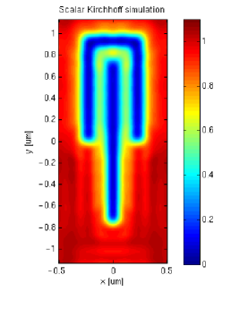 (c)
(c)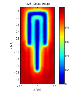
Similar equations are found for the electric field ; these are treated accordingly. The finite-element method solves Eqs. (1) – (4) in their weak form, i.e., in an integral representation. The computational domain is discretized with triangular (2D) or tetrahedral/prismatoidal (3D) patches. The use of prismatoidal patches is well suited for layered geometries, as in photomask simulations. This also simplifies the geometry description of the mask layout. Sidewall angles different from 90 deg are not regarded throughout this paper; however, they can easily be implemented with reasonable restrictions. The function spaces are discretized using Nedelec’s edge elements, which are vectorial functions of polynomial order (here, first to fourth order) defined on the triangular or tetrahedral patches [10]. In a nutshell, FEM can be explained as expanding the field corresponding to the exact solution of Equation (1) in the basis given by these elements. This leads to a large sparse matrix equation (algebraic problem). For details on the weak formulation, the choice of Bloch-periodic functional spaces, the FEM discretization, and our implementation of the PML method we refer to previous works [7, 5, 11]. In future implementations performance will further be increased by using higher order elements, , -adaptive methods, and by using elements of different polynomial order parallel and orthogonal to the layers of the layered geometry (corresponding to the plane of Fig. 4 b). To solve the algebraic problem on a standard workstation either standard linear algebra decomposition techniques (LU-factorization, e.g., package PARDISO [12]) or iterative and domain decomposition methods [13, 14, 15] are used, depending on problem size. Domain decomposition methods as shown in Ref. [14] for 2D FEM simulations can be easily transferred to layered 3D geometries (typical photomask geometries) and other 3D geometries. Due to the use of multi-grid algorithms, the computational time and the memory requirements grow linearly with the number of unknowns.
2 3D Simulations
We investigate a 3D test structure as schematically depicted in Figure 1. The structure consists of MoSi-lines of height with a sidewall angle of 90 deg on a glass substrate. This pattern was chosen to have low vector and interference effects but still significant 3D effects, and because it appears in current lithography production. With the project parameters as given in Table 1 the size of the computational domain is around cubic wavelengths. We discretize the computational domain using prismatoidal patches, and we use higher order, vectorial ansatz functions as finite elements defined on these patches.
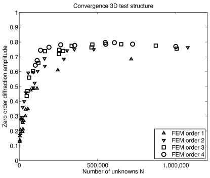
Figure 3 shows the convergence of the simulated zero order far field coefficient. Plotted is the magnitude of the far field coefficient vs. number of degrees of freedom of the finite element expansion. Data points are attained using finite elements of first, second, third, and fourth polynomial order and using meshes with different refinement levels. With increasing finite element degree and with decreasing mesh size the results converge. From these results we guess the relative error for a solution using fourth order finite elements and using about unknowns is of the order of .
To model illumination with a realistic source we construct a grid of source points in wavevector-space. For each source point we define two plane waves with orthogonal polarizations. This makes a total of 462 sources. In order to obtain the scattering response of an extended, measured C-Quad source we linearly interpolate the results for each measured source point between the closest simulated source points and superpose the results. JCMharmony allows to calculate the scattering response of all of the 462 sources in a single programme run. The total computation time on a workstation (2 64bit processors, around 20 GB RAM) to obtain the 462 near field solutions, each with 482,040 degrees of freedom, was around 100 minutes. We currently work on the significant reduction of the near field computation time.
A simulation on this area is impossible with present Solid-E 3.3 or Prolith 9.1 even for a single illumination direction due to memory consumption at necessary resolution. Also the simulation time with unacceptable coarse grids is orders of magnitude higher.
We use the far field coefficients to generate an aerial image. Figure 2 a) shows a pseudo color representation of the intensity distribution in the image plane (demagnification factor 4). The scalar intensity distribution has been obtained from the vectorial electric field distribution. Figure 2 b) shows a similar intensity distribution obtained using a non-rigorous method (Kirchhoff approximation). Obviously, the approximation compares well with the rigorous solution for this specific simulation example. I.e., interference effects, high-NA effects or other effects do not play a role here. This example was rather chosen to demonstrate the applicability of a rigoros method to large 3D problems.
Figure 2 c) shows an experimentally obtained aerial image obtained using AIMS. The minima in the experimental aerial image of the mask structure are more pronounced than in the simulation. This can be, e.g., caused by uncertainties in the geometry of the sample. As has been shown in different works [16] the high accuracy and speed of rigorous FEM simulations can be utilized to obtain precise informations about the sample geometry or material parameters by optimizing the deviation from experimentally obtained data.
3 Validation of the Results
In order to validate the results of the FEM solver we have performed several tests. Here we present 3D simulations of line masks and compare the results to results using 2D simulations of the same physical settings. For these we have we have investigated the convergence towards results obtained with various methods, as reported earlier [2].
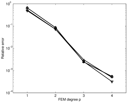
Figure 4 shows a schematics of the geometry of a periodic line mask. TM polarized light is incident from the substrate and is diffracted into various diffraction orders. The geometry parameters are listed in Table 1 (data set 2). Please see Reference [2] for more details on this test case. The 2D simulation results given in the first line of Table 2 are the best converged results from this reference for the given test case. We therefore refer to these results as ’quasi-exact’ results. Table 2 further shows results obtained with 3D FEM on the geometry as depicted in Figure 4 b). Vectorial finite elements of order 1 to 4 on grids with different mesh refinements have been used to obtain rigorous near field solutions from which the zero order far field coefficients are obtained. As expected and as can be seen from the results, most accurate results are obtained using elements of high order and fine meshes. Figure 5 shows the convergence of the results on several fixed FEM grids with elements of increasing polynomial order. As expected, with increasing polynomial order the numerical approximation error converges exponentially towards zero.
| JCMharmony 2D (TM) | ||||
|---|---|---|---|---|
| -0.21943 | 0.27179 | 0.34932 | ||
| JCMharmony 3D, first order elements (TM) | ||||
| n | N | |||
| 1 | 470 | -0.15665 | 0.03066 | 0.15963 |
| 1 | 2230 | -0.17802 | 0.09517 | 0.20186 |
| 1 | 9821 | -0.23282 | 0.23871 | 0.33345 |
| 1 | 35741 | -0.21775 | 0.26485 | 0.34287 |
| 1 | 84139 | -0.22011 | 0.26071 | 0.34120 |
| 1 | 299690 | -0.21847 | 0.26942 | 0.34687 |
| JCMharmony 3D, second order elements (TM) | ||||
| n | N | |||
| 2 | 1884 | -0.26261 | 0.22353 | 0.34486 |
| 2 | 13672 | -0.22516 | 0.26312 | 0.34631 |
| 2 | 54398 | -0.21984 | 0.26810 | 0.34671 |
| 2 | 99468 | -0.21885 | 0.27110 | 0.34841 |
| 2 | 376786 | -0.21910 | 0.27145 | 0.34884 |
| JCMharmony 3D, third order elements (TM) | ||||
| n | N | |||
| 3 | 5652 | -0.22476 | 0.26408 | 0.34678 |
| 3 | 27264 | -0.21862 | 0.27199 | 0.34896 |
| 3 | 139659 | -0.21971 | 0.27199 | 0.34964 |
| JCMharmony 3D, fourth order elements (TM) | ||||
| n | N | |||
| 4 | 12608 | -0.21726 | 0.27308 | 0.34896 |
| 4 | 100036 | -0.21902 | 0.27154 | 0.34886 |
| 4 | 365384 | -0.21931 | 0.27170 | 0.34917 |
4 Conclusions
We have performed rigorous 3D FEM simulations of light transition through a large 3D photomask (size of the computational domain about 1000 cubic wavelengths). We have achieved results at high numerical accuracy which compare well to experimental findings using aerial imaging. We have checked the convergence for this 3D case and we have checked the convergence of the method for a simpler case, where a quasi-exact result is available. Our results show that rigorous 3D mask simulations can well be handled at high accuracy and relatively low computational cost.
Acknowledgements.
We thank Arndt C. Dürr (AMTC Dresden) for the AIMS measurement. The work for this paper was supported by the EFRE fund of the European Community and by funding of the State Saxony of the Federal Republic of Germany (project number 10834). The authors are responsible for the content of the paper.References
- [1] A. Erdmann, “Process optimization using lithography simulation,” Proc. SPIE 5401, p. 22, 2004.
- [2] S. Burger, R. Köhle, L. Zschiedrich, W. Gao, F. Schmidt, R. März, and C. Nölscher, “Benchmark of FEM, waveguide and FDTD algorithms for rigorous mask simulation,” in Photomask Technology, J. T. Weed and P. M. Martin, eds., 5992, pp. 378–389, Proc. SPIE, 2005.
- [3] C. Enkrich, M. Wegener, S. Linden, S. Burger, L. Zschiedrich, F. Schmidt, C. Zhou, T. Koschny, and C. M. Soukoulis, “Magnetic metamaterials at telecommunication and visible frequencies,” Phys. Rev. Lett. 95, p. 203901, 2005.
- [4] S. Burger, L. Zschiedrich, R. Klose, A. Schädle, F. Schmidt, C. Enkrich, S. Linden, M. Wegener, and C. M. Soukoulis, “Numerical investigation of light scattering off split-ring resonators,” in Metamaterials, T. Szoplik, E. Özbay, C. M. Soukoulis, and N. I. Zheludev, eds., 5955, pp. 18–26, Proc. SPIE, 2005.
- [5] S. Burger, R. Klose, A. Schädle, and F. S. and L. Zschiedrich, “FEM modelling of 3d photonic crystals and photonic crystal waveguides,” in Integrated Optics: Devices, Materials, and Technologies IX, Y. Sidorin and C. A. Wächter, eds., 5728, pp. 164–173, Proc. SPIE, 2005.
- [6] T. Kalkbrenner, U. Hakanson, A. Schädle, S. Burger, C. Henkel, and V. Sandoghdar, “Optical microscopy using the spectral modifications of a nano-antenna,” Phys. Rev. Lett. 95, p. 200801, 2005.
- [7] L. Zschiedrich, R. Klose, A. Schädle, and F. Schmidt, “A new finite element realization of the Perfectly Matched Layer Method for Helmholtz scattering problems on polygonal domains in 2D,” J. Comput. Appl. Math. 188, pp. 12–32, 2006.
- [8] T. Hohage, F. Schmidt, and L. Zschiedrich, “Solving Time-Harmonic Scattering Problems Based on the Pole Condition I: Theory,” SIAM J. Math. Anal. 35(1), pp. 183–210, 2003.
- [9] K. Sakoda, Optical Properties of Photonic Crystals, Springer-Verlag, Berlin, 2001.
- [10] P. Monk, Finite Element Methods for Maxwell’s Equations, Claredon Press, Oxford, 2003.
- [11] L. Zschiedrich, S. Burger, R. Klose, A. Schädle, and F. Schmidt, “JCMmode: an adaptive finite element solver for the computation of leaky modes,” in Integrated Optics: Devices, Materials, and Technologies IX, Y. Sidorin and C. A. Wächter, eds., 5728, pp. 192–202, Proc. SPIE, 2005.
- [12] O. Schenk et al., “Parallel sparse direct linear solver PARDISO.” Department of Computer Science, Universität Basel.
- [13] P. Deuflhard, F. Schmidt, T. Friese, and L. Zschiedrich, Adaptive Multigrid Methods for the Vectorial Maxwell Eigenvalue Problem for Optical Waveguide Design, pp. 279–293. Mathematics - Key Technology for the Future, Springer-Verlag, Berlin, 2003.
- [14] L. Zschiedrich, S. Burger, A. Schädle, and F. Schmidt, “Domain decomposition method for electromagnetic scattering problems,” in Proceedings of the 5th International Conference on Numerical Simulation of Optoelectronic devices, pp. 55–56, 2005.
- [15] A. Schädle, L. Zschiedrich, S. Burger, R. Klose, and F. Schmidt, “Domain decomposition method for Maxwells equations: Scattering off periodic structures,” Tech. Rep. 06-04, Zuse-Institute Berlin, 2006.
- [16] J. Pomplun, S. Burger, F. Schmidt, L. W. Zschiedrich, F. Scholze, and U. Dersch, “Rigorous FEM-simulation of EUV-masks: Influence of shape and material parameters,” in Photomask Technology, Proc. SPIE 6349-128, 2006.