A unifying approach to left handed material design
Abstract
In this letter we show that equivalent circuits offer a qualitative and even quantitative simple explanation for the behavior of various types of left-handed (or negative index) meta-materials. This allows us to optimize design features and parameters, while avoiding trial and error simulations or fabrications. In particular we apply this unifying circuit approach in accounting for the features and in optimizing the structure employing parallel metallic bars on the two sides of a dielectric film. Pacs: 42.70.Qs, 41.20.Jb, 42.25.Bs, 73.20.Mf
Left-handed materials exhibit a negative permeability, , and permittivity, , over a common frequency range Veselago (1968). Negative permeability is the result of a strong resonance response to an external magnetic field; negative permittivity can appear either by a plasmonic or a resonance response (or both) to an external electric field. Negative and negative lead to negative index of refraction, , and to a left-handed triad of ; hence, the names negative index materials (NIMs) or Left-handed Materials (LHMs). PendryPendry et al. (1996, 1999) suggested a double metallic split-ring resonator (SRR) design for negative and a parallel metallic wire periodic structure for an adjustable plasmonic response. Several variation of the initial design have been studied; among them a single ring resonator with several cuts has been proved capable of reaching negative at higher frequency Zhou et al. (2005); in Fig. 1(a) a two cut single ring is shown schematically. This, by a continuous transformation, can be reduced to a pair of carefully aligned metal bars separated by a dielectric spacer of thickness Zhou et al. (2006a); Shalaev et al. (2005); in Figs 1(b) and 1(c) the view in the () and () planes of this structure is shown together with the directions of of the incoming field.
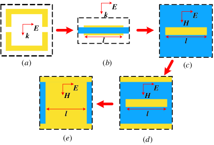
The design shown in Figs 1(b,c), besides its simplicity, has distinct advantages over conventional SRRs. The incident electromagnetic wave is normal to the structure as shown in Fig. 1(b), which enable us to build NIMs by only one layer of sample and achieve relatively strong response. Conventional SRRs, although they exhibit magnetic resonance which may produce negative , they fail to give negative at the same frequency range and, hence, they are incapable by themselves to produce NIMs. An extra continuous wire is needed to obtain negative via plasmonic response Pendry et al. (1996); Smith et al. (2000). In contrast, the pair of parallel metallic plates is expected to exhibit not only a magnetic resonance [Fig. 2(c), antisymmetric mode], but to show an electric resonance as well [symmetric mode] properly located in frequency by adjusting the length, , of the pair.
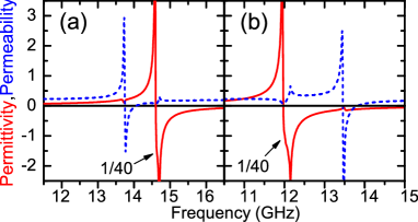
The simulations were done with the CST Microwave Studio (Computer Simulation Technology GmbH, Darmstadt, Germany) using the lossy metal model for copper with a conductivity for a single unit cell with periodic boundary in the (E,H) plane, field distribution and scattering amplitudes have been calculated. The in Fig. 6 have been obtained by a retrieval procedure Smith et al. (2002). At the magnetic resonance the two plates sustain anti-parallel currents producing a magnetic field confined mainly in the space between the plates and directed opposite to that shown in Fig. 1(c); the electric field, because of the opposite charges accumulated at the ends of the two plates, is expected to be confined within the space between the plates and near the end points. Indeed, detailed simulations, shown in Fig. 2(c), confirm this picture.
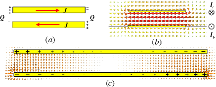
At the electric resonance the currents at the two bars are parallel (symmetric mode); the magnetic field lines go around both bars, while the electric field is mostly confined in the space between the nearest neighbor edges of the two pairs of bars belonging to consecutive unit cells.
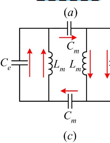
The field and current configurations for both the antisymmetric and the symmetric mode can be accounted for by equivalent circuits as shown in Fig. 3 (in which for simplicity the resistor elements have been omitted). Near the magnetic resonance frequency where the current configuration is as in Fig. 3(c), the magnetic field is between the two plates and it is, to a good approximation, uniform (Fig. 2(b)). Hence the total inductance , as calculated by the magnetic field energy, is
| (1) |
where is the length of the wire, is the thickness of the dielectric spacer and is the width of the wire.
Notice that at telecommunication or optical frequencies, where the linear dimension are in the tens or hundreds of nm, the kinetic energy of the drifting electrons makes a contribution comparable or larger than the magnetic energy. Hence, another additional inductance must be added to the right hand side of Eq.1 Zhou et al. (2005).
Each of the capacitance must be given by a formula of the type
| (2) |
where by inspection of Fig. 2(c), with the numerical factor in the range . The capacitance can be approximated by that of two parallel wires of radius and length at a distance apart
| (3) |
where is the thickness of each metallic bar and is the separation of neighboring pairs Fig. 3(a,b) (). The magnetic resonance frequency, , is obtained by equating the impedance (of and in parallel) with minus the impendence of the capacitance .
Since we obtain
| (4) |
The last relation follows because, for the values we have used ( and ), . Combining the Eq.1 and Eq.2 we find that
| (5) |
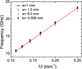
where is the reduced dielectric constant of the dielectric, . In Fig.4 we compare our result of Eq.5, which shows that is a linear function of only , with detailed simulations results. Fig. 4 shows the dependence of the magnetic resonance frequency as obtained from the retrieved resonant effective on the inverse length of the parallel metallic bars (Fig. 1b), for different widths (separation between parallel bars fixed) and two different separations (width of bars fixed). Complete quantitative agreement is obtained if . Notice the independence of the simulation results on the width and the dielectric thickness . It is worthwhile to point out that the result is robust over a wide range of parameters even if Eqs. 1 and 2 are not valid. To see this point, consider the extreme case of a pair of thin wires (as opposed to a pair of bars) of length , cross-section radius , at a distance apart such that . For such a system and . Thus again .
For frequencies near the electric resonance, because of mirror symmetry in Fig. 3(d), there is no current passing through the capacitances . As a results the electric resonance frequency is given by , where is expected to be of the form where is a function which for behaves as .
We point out that is a rather sensitive function of the small distance , because depends on , while is practically independent on . Indeed the ratios and for according to the equation of and equation of are respectively and in good agreement with the simulation results in Fig. 5 ( and respectively); the dependence of both and on is shown in Fig. 5.
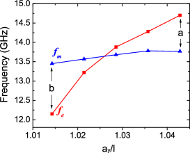
Fig. 5 in combination with Fig. 6 suggest the optimum design parameters for making the two bar scheme to produce negative index : One has to avoid the crossing region where essentially to a considerably degree the two resonances cancel each other. Since the electric resonance is much stronger and, hence, much wider we have to bring the magnetic resonance within the negative region of , i.e. we must have lower than as in Fig. 6(b), rather that the other way around, i.e. we must have
| (6) |
This can be achieved by increasing either by decreasing or by increasing at the ends of each bar the width choosing a double shape for each bar Zhou et al. (2006b).
Still another possibility to make the negative region wider (and more negative) is to add continuous metallic wires as in Fig. 1(d) which produce a plasmonic response Zhou et al. (2006a). By adjusting the width of these wires their effective plasma frequency can be made larger than the frequency, , at which the continuous curve in Fig. 6(b) crosses the axis ().
Finally the width of the bars, , can increase until the bars join the ”infinite” wires producing thus a continuous connected network which can be constructed by opening periodically placed rectangular holes on uniform metallic films covering both sides of a dielectric sheet Dolling et al. (2006); Zhang et al. (2005a, b).
In this letter we have shown that equivalent circuits can account for the properties of various negative index artificial meta-materials (NIMs), even at a quantitative level; furthermore, this simple unifying circuit approach offers a clear guidance in adjusting the design and optimizing the parameters for existing and possibly, future NIMs.
We gratefully acknowledge the support of Ames Laboratory (operated by Iowa State University under Contract No. W-7405-Eng-82), the AFOSR under MURI grant (FA9550-06-1-0337), EU Network of Excellence projects METAMORPHOSE and PHOREMOST, and Defence Advanced Research Projects Agency (DARPA) contract HR0011-05-C-0068).
References
- Veselago (1968) V. Veselago, Sov.Phys. Usp. 10, 509 (1968).
- Pendry et al. (1996) J. Pendry, A. Holden, W. Stewart, and I. Youngs, Physical Review Letters 76, 4773 (1996).
- Pendry et al. (1999) J. Pendry, A. Holden, D. Robbins, and W. Stewart, IEEE Trans. Microwave Theroy Tech. 47, 2075 (1999).
- Zhou et al. (2005) J. Zhou, T. Koschny, M. Kafesaki, E. N. Economou, J. B. Pendry, and C. M. Soukoulis, Physical Review Letters 95, 223902 (pages 4) (2005), URL http://link.aps.org/abstract/PRL/v95/e223902.
- Zhou et al. (2006a) J. Zhou, L. Zhang, G. Tuttle, T. Koschny, and C. M. Soukoulis, Physical Review B (Condensed Matter and Materials Physics) 73, 041101 (pages 4) (2006a), URL http://link.aps.org/abstract/PRB/v73/e041101.
- Shalaev et al. (2005) V. M. Shalaev, W. S. Cai, U. K. Chettiar, H. K. Yuan, A. K. Sarychev, V. P. Drachev, and A. V. Kildishev, Optics Letters 30, 3356 (2005).
- Smith et al. (2000) D. Smith, W. Padilla, D. Vier, S. Nemat-Nasser, and S. Schultz, Physical Review Letters 84, 4184 (2000).
- Smith et al. (2002) D. R. Smith, S. Schultz, P. Markos, and C. M. Soukoulis, Physical Review B (Condensed Matter and Materials Physics) 65, 195104 (pages 5) (2002), URL http://link.aps.org/abstract/PRB/v65/e195104.
- Zhou et al. (2006b) J. Zhou, T. Koschny, L. Zhang, G. Tuttle, and C. M. Soukoulis, Applied Physics Letters 88, 221103 (pages 3) (2006b), URL http://link.aip.org/link/?APL/88/221103/1.
- Dolling et al. (2006) G. Dolling, C. Enkrich, M. Wegener, C. M. Soukoulis, and S. Linden, Science 312, 892 (2006).
- Zhang et al. (2005a) S. Zhang, W. Fan, B. K. Minhas, A. Frauenglass, K. J. Malloy, and S. R. J. Brueck, Physical Review Letters 94, 037402 (pages 4) (2005a), URL http://link.aps.org/abstract/PRL/v94/e037402.
- Zhang et al. (2005b) S. Zhang, W. Fan, N. C. Panoiu, K. J. Malloy, R. M. Osgood, and S. R. J. Brueck, Physical Review Letters 95, 137404 (pages 4) (2005b), URL http://link.aps.org/abstract/PRL/v95/e137404.