Analysis of surface waves generated on subwavelength-structured silver films
Abstract
Using transmission electron microscopy (TEM) to analyse the physical-chemical surface properties of subwavlength structured silver films and finite-difference time-domain (FDTD) numerical simulations of the optical response of these structures to plane-wave excitation, we report on the origin and nature of the persistent surface waves generated by a single slit-groove motif and recently measured GAV06a by far-field optical interferometry. The surface analysis shows that the silver films are free of detectable oxide or sulfide contaminants, and the numerical simulations show very good agreement with the results previously reported.
pacs:
42.25.Fx. 73.20.Mf. 78.67.-nI Introduction
The optical response of subwavelength-structured metallic films has enjoyed a resurgence of interest in the past few years due to the quest for an all-optical solution to the inexorable drive for ever-smaller, denser integrated devices operating at ever-higher band width IPRA-Nano . Two basic questions motivate research in this field: how to confine micron-sized light waves to subwavelength dimensions DSA06 and how to transmit this light without unacceptable loss over at least tens of microns ZSB05 ; BDE03 . Although surface waves and in particular periodic arrays of surface plasmon polaritons (SPPs) have received a great deal of attention as promising vehicles for subwavelength light confinement and transport, detailed understanding of their generation and early time evolution (within the first few optical cycles) in and on real metal films is still not complete XZM04 ; ZMM06 ; QL02 ; LHR05 . Recent measurements GAV06a ; GAV06b of far-field interference fringes arising from surface wave generation in single slit-groove structures on silver films have characterized the amplitude, wavelength and phase of the surface waves. After a rapid amplitude decrease within the first three microns from the generating groove, waves persisting with near-constant amplitude over tens of microns were observed. Such long-range transport is the signature of a ”guided mode” SPP, but the measured wavelength was found to be markedly shorter than the expectation from conventional theory Raether . One possible reason advanced for the disparity between experiment and theory was the presence of an oxide or sulfide dielectric layer on the silver surface, and it has been suggested LH06 that an 11 nm layer of silver sulfide would bring experiment and theory into agreement. We report here the results of two investigations: one experimental, into the physical-chemical surface properties of the silver structures with the intent of detecting the presence of a dielectric layer and the other theoretical, into the calculated optical response of the untarnished silver slit-groove structures using the FDTD technique to numerically solve Maxwell’s equations. These studies shown no evidence of oxide or sulfide layers on the silver surface and the numerical solutions to Maxwell’s equations show good agreement with measurements reported in GAV06a .
II TEM analysis of structured silver surfaces
Three typical structured samples were chosen for examination with fabrication dates of about 12 months, 6 months, and 1 week from the date of the TEM analysis. The structures dating from 6 months and 12 months were part of the series of structures actually used in the previous reports GAV06a ; GAV06b . The subwavelength structures consist of a 400 nm silver film evaporated onto a fused silica substrate (Corning 7980 UV grade© 25 mm square, 1 mm thick optically polished on both sides to a roughness of no more than 0.7 nm). The structured substrates are stored in Fluoroware® sample holders, 25 mm diameter and 1 mm in depth at the center.
II.1 Methods
Electron transparent sections for cross-sectional transmission electron microscopy (TEM) examination were prepared by sample thinning to electron transparency using standard focused Ga+-ion beam (FIB) milling procedures milling in a FEI 200 FIB workstation and placed on a holey carbon support. The TEM characterization was performed using a Philips CM300 Schottky field emission gun (FEGTEM) microscope operating at 300 kV. The field emission electron source is ideal for applications requiring high coherency, high brightness at high magnification, or small focused probes of selected areas. The FEGTEM has a point resolution of 0.2 nm and an information limit of 0.12 nm. The minimum focused electron beam probe size is 0.3 nm. In dark field images, one or more diffracted beams are allowed to pass the objective aperture while the direct straight-through beam is blocked by the aperture. In contrast to the direct beam, the diffracted beam interacts strongly with the specimen and selection of a particular diffracted beam allows better visual phase differentiation.
II.2 Examination of silver (Ag) layers
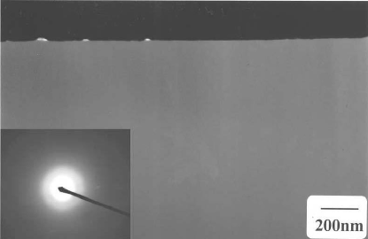
Typical regions of Ag layer that were thinned to electron transparency are shown at relatively low magnification in the bright field micrograph in Fig. 1. An immediate distinction can be made between the fused silica substrate (A) and the Ag deposit (B). Protective capping layers of Au and Pt, applied at the time of analysis, are marked at (C) and (D) respectively. The latter are used to prevent any ‘top down’ ion damage of the cross-section during the ion beam thinning preparation.
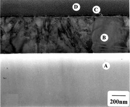
The white colored line marked by an arrow in Fig. 1 and shown in more detail in Fig. 3 is a band that contains very fine particles of Au that are formed during the initial stages of the deposition of this metal.
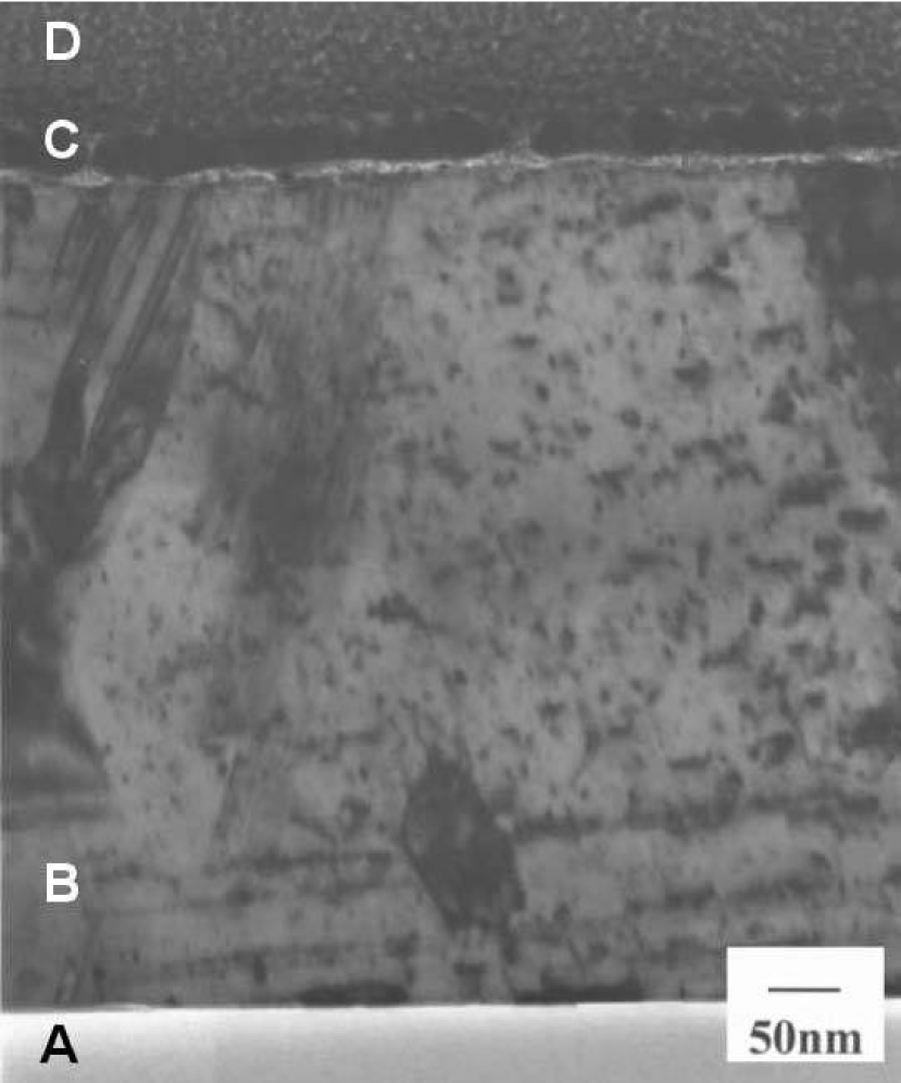
The fine particles do not exhibit the same degree of absorption contrast as the bulk of the Au formed above them because the particle diameters are less than the thickness of the cross-sectional slice and thus do not extend through the full thickness of the TEM sample, as do the relatively coarse grains constituting the bulk of the Au protection layer. A higher magnification TEM micrograph of this region is shown for clarity in Fig. 3. It is clearly observed that the Au nanoparticles form a separate layer above the Ag deposit and any local undulations in the Ag layer are observed to be devoid of any oxide or sulfide layer.
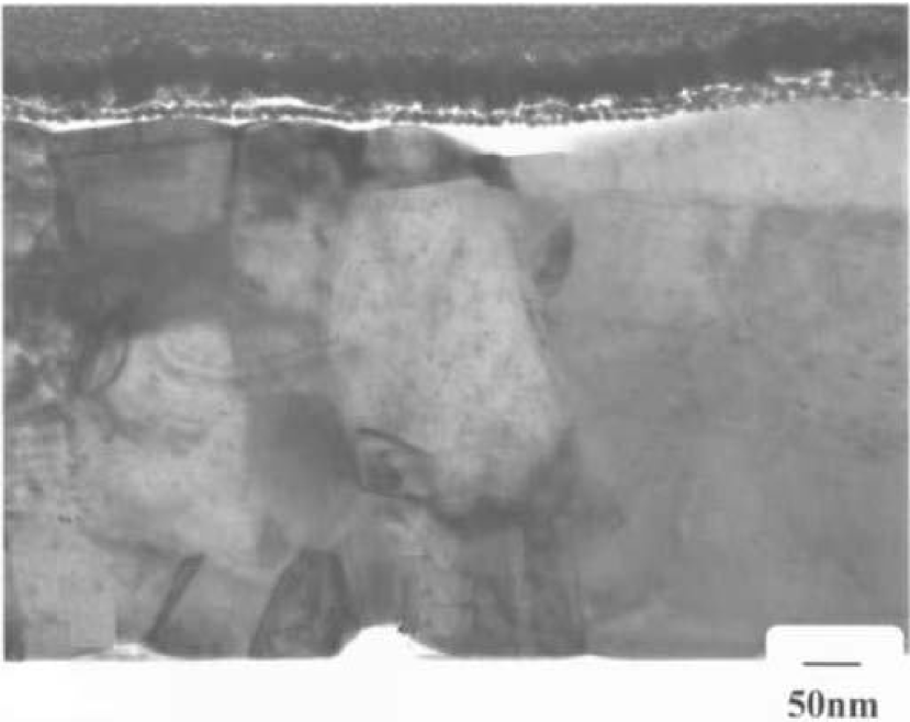
Fresnel contrast methods were used to examine the upper surface regions of the silver in more detail and a typical area is shown in Fig. 4.
Imaging of layers in cross-section, in which the electrons travel parallel to the interfaces between the two materials, always results in Fresnel fringes. Because the amplitude and phase changes that occur when an electron is scattered elastically are characteristic of the atomic number, there will be changes in the elastic scattering directly related to the form of the projected scattering potential when there is a composition change at an interface viewed in projection wang , analogous to a phase grating filtering of the scattered electronic wave function. Interface Fresnel effects can thus provide a signature on the form and magnitude of any compositional discontinuity that is present. The visibility of these fringes depends on the thickness of the specimen and on the defocus value of the microscope. The contrast of the fringes is higher with increasing defocus, at both positive and negative values from the minimum contrast condition. From Fig. 4, the critical observation is in the absence of Fresnel effects at the surface of the metal as a function of focus conditions other than at the localized regions associated with the gold protective coating. The lack of Fresnel fringes at the upper surface indicates a lack of variation in the scattering potentials and hence of the chemistry or the composition at the interface. The lack of Fresnel signature demonstrates that silver surface is not covered by a detectable layer of sulfide or oxide since their presence would exhibit differences in scattering potential by comparison with the metal itself fultz . The lower detection limit for such compositional differences is a few tenths nanometer layer thickness.
II.3 Discussion of the surface analysis
The high resolution TEM analysis failed to detect the presence of oxide or sulfide coating on any of the structured silver samples. This result is in fact not surprising and is consistent with a simple estimate of the surface chemical impurity likely to be present. Since the structures are kept in air-tight sample holders, the total,static volume of air to which they are exposed during storage is mm3. The trace fractional concentrations of sulfur dioxide and hydrogen sulfide in ordinary laboratory air is less than BPB69 and therefore about impurity molecules are available to react with the 625 mm2 silver surface. The average linear distance between impurity molecules, assuming all of them reacted with the surface, is therefore about 250 nm – a surface density below the detection limit of the FEGTEM instrument.
For comparison, TEM was also conducted on a similar Ag structure left fully exposed to ambient laboratory environment for more than two years. The resulting micrograph and electron diffraction pattern are shown in Fig. 5. The tarnished Ag layer is observed to be uniform and the corresponding electron diffraction data shows a fully amorphous (noncrystalline) character evidenced by the broad diffuse rings. The detection of a relatively high intensity signal from a nominally nondiffracting material yields valuable information on not only the crystallinity of the material, but also the chemical composition. Comparing the electron diffraction data for the tarnished samples to that for the silver structures described earlier, we find no evidence of a similar noncrystalline material on the surface of the untarnished Ag shown in Fig. 1.
III Calculation of the far-field transmission
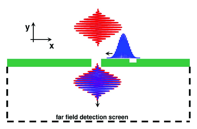
The optical response of structured metal surfaces is simulated using a finite-difference-time-domain (FDTD) approach Taflove2000 . The subwavelength slit-groove structures GAV06a ; GAV06b can be modelled in two dimensions, and we consider here the case of transverse magnetic TM polarization (with the -field transverse to the plane of incidence and parallel to the long axis of the slit-groove structures). The set-up for the simulations is shown in Fig. 6.
The Maxwell equations are thus,
| (1) | |||||
where , , and are the Cartesian components of the electric and magnetic fields, and are the Cartesian components of the current density , is the electric permittivity and is the magnetic permeability of free space. In metallic regions of space is a complex valued, frequency-dependent function. Within the standard Drude model Huffman1983 it is given as,
| (2) |
where is the electric permittivity of free space, is the dimensionless infinite frequency limit of the dielectric constant, is the bulk plasmon frequency, and is the damping rate. In order to properly describe the material dispersion of the metal structures we numerically fit the real and imaginary parts of the Drude dielectric constant in the form of Eq. 2 to the experimental data collected in LynchHunter . The Drude parameters obtained in the wavelength regime ranging from nm to nm for silver are , rad s-1, and rad s-1, which correspond to and at nm. These fitted parameters are close to those determined in GAV06a by ellipsometry, and . Numerical results were not sensitive to this range of parameter variability.
The frequency dependence of the dielectric constant Eq. 2 results in an additional equation to the Maxwell equations (1), describing the time evolution of the current density in the metallic region of space Ziolkowski1995 .
| (3) |
where , and . In the surrounding free space , and and hence vanishes Gray2003PRB .
As a reference for the optical response of the Drude metal we also implement perfect electric conductor (PEC) boundary conditions, where the metal dielectric constant is set to negative infinity, and all electromagnetic field components are therefore strictly zero in metal regions.
The light source is a plane wave, incident perpendicular to the metal surface and depending on time as,
| (4) |
where is the peak amplitude of the pulse, is the pulse envelope, and is the pulse duration (.
Time propagation of Eqs. 1, 3 is performed by a leapfrogging technique Taflove2000 . In order to prevent nonphysical reflection of outgoing waves from the grid boundaries, we employ perfectly matched layer (PML) absorbing boundaries, within which is split into two additive subcomponents BerengerPML . To avoid accumulation of spurious electric charges at the ends of the excitation line and generate a pure plane wave with a well-defined incident wavelength, we embed the ends in the PML regions. We have tested this approach by direct comparison with the total field/scattered field technique Taflove2000 . In all simulations the spatial grid ranges from m to m and m to m. Convergence is achieved with a spatial step size of nm and a temporal step size of , where denotes the speed of light in vacuum.
All simulations have been performed on distributed memory parallel computers at the National Energy Research Scientific Computing Center and San Diego Supercomputer Center. The parallel technique used in our simulations is described in detail in SukharevJCP2006 .
III.1 Numerical results
Calculations of the intensity, , are performed along a box contour as shown in Fig. 6, including a line parallel to the metal surface and located at the distance . The collected data is averaged over time and the spatial coordinates for a range of slit-groove distances. Finally, the space- and time-averaged intensity is normalized to unit maximum. Our results converge with m and are invariant to the pulse duration (hence converged to the CW limit) with incident pulse durations fs. A direct comparison of the experimental data with both the PEC and the Drude models is shown in Fig. 7.
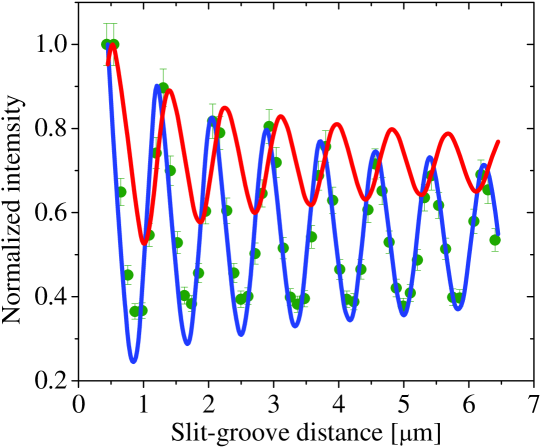
Clearly, the Drude model agrees very well with the data, whereas the PEC model predicts oscillations of the intensity with a noticeably larger wavelength and smaller amplitude. In order to properly determine the wavelength of oscillations we use a function with an exponentially decreasing amplitude component and constant offset to fit the data shown in Fig. 7 and extend both the FDTD simulation and the fitting function to a slit-groove distance of 16 m, well beyond the range of experimental data. We then take the Fourier transform of the fitted function over this extended range to obtain the associated power spectrum expressed as a wavelength distribution. The results are shown in Fig. 9.
| (5) |
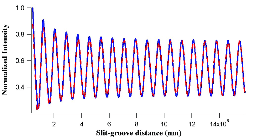
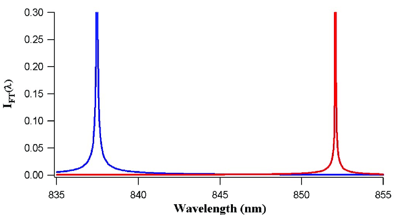
The FDTD simulation and analytic fit for larger slit-groove distances are shown in Fig. 9 for the case of the Drude model. The fitting function Eq. 5 tracks reasonably well the FDTD results over the entire slit-groove distance range. Figure 9 shows the normalized power spectrum corresponding to Eq. 5 as a function of the wavelength. The two power spectrum plots of Fig. 9 provide the effective wavelength, , at which surface waves propagate as well as the distribution of modes around the peak. Note that the Drude model for silver shows a marked blue shift in peak wavelength and a noticeable broadening of the distribution compared to the perfect metal PEC model. The Drude model results in nm , whereas PEC model gives nm, very close to the free-space reference wavelength nm. The effective surface index of refraction
| (6) |
where is the incident wavelength (in the experiment nm), leads to the following values: and .
IV Summary and conclusions
Surface analysis by transmission electron microscopy of subwavelength structured silver films used to investigate their optical response GAV06a ; GAV06b showed no detectable evidence of material on the surface other than silver. The suggestion that an 11 nm sulfide layer may be present so as to bring the interference pattern calculated by the authors of Ref. LH06 into agreement with experiment is therefore not confirmed.
In contrast to the calculations reported by Ref. LH06 , numerical solution of Maxwell’s equations reported here using an FDTD approach does show very good agreement with the fringe amplitude and wavelength over the slit-groove range of the data reported in GAV06a . Extrapolation of the FDTD simulations beyond the range of the measurements shows that the initially decreasing amplitude of the fringe settles to an oscillation with near-constant amplitude and fringe contrast. These features resemble the calculations of LH06 , but the results reported here show much better agreement with experiment without the need to invoke an 11 nm silver sulfide layer. Fourier analysis of the FDTD simulations reveal that the most probable wavelength in the Fourier distribution is 837 nm, within a about 2 nanometers of the expected long-range SPP wavelength of 839 nm. The reasons for the discrepancies between the results of Ref. LH06 , which employ a different approach using rigorous-coupled-wave-analysis (RCWA) and those reported here have not yet been identified.
Acknowledgements.
Support from the Ministère délégué à l’Enseignement supérieur et à la Recherche under the programme ACI-“Nanosciences-Nanotechnologies,” the Région Midi-Pyrénées [SFC/CR 02/22], and FASTNet [HPRN-CT-2002-00304] EU Research Training Network, is gratefully acknowledged as is support from the Caltech Kavli Nanoscience Institute and from the AFOSR under Plasmon MURI FA9550-04-1-0434. This research used resources of the National Energy Research Scientific Computing Center, which is supported by the Office of Science of the U.S. Department of Energy under Contract No. DE-AC03-76SF00098, and San Diego Supercomputer Center under Grant No. PHY050001. Discussions with P. Lalanne, M. Mansuripur, and H. Atwater as well as computational assistance from J. Yelk and Y. Xie are also gratefully acknowledged.References
- (1) G. Gay, O. Alloschery, B. Viaris de Lesegno, C. O’Dwyer, J. Weiner and H. J. Lezec, Nature Physics 2, 262-267 (2006).
- (2) See for example the Technical Digest of the Integrated PHotonics Research and Application (IPRA) and Nanophotonics (Nano) topical meetings of the Optical Society of America, Uncasville, Connecticut USA, April 24-28, 2006 (ISBN 1-55752-807-1).
- (3) J. A. Dionne, L. A. Sweatlock, H. A. Atwater and A. Polman, Phys. Rev. B 73, 035407-1–9 (2006) and references cited therein.
- (4) R. Zia, M. D. Selker, and M. L. Brongersma, Phys. Rev. B 71 16543-1–9 (2005).
- (5) W. L. Barnes, A. Dereux, and T. W. Ebbesen, Nature (London) 424, 824-830 (2003) and references cited therein.
- (6) Y. Xie, A. Z. Zakharian, J. V. Moloney, and M. Mansuripur, Opt. Express 13 4485-4491 (2005).
- (7) A. R. Zakharian, J. V. Moloney, and M. Mansuripur, Surface plasmon polaritons on metallic surfaces, unpublished.
- (8) Q. Cao and P. Lalanne, Phys. Rev. Lett. 88, 057403 (2002).
- (9) P. Lalanne, P. Hugonin, and J. C. Rodier, Phys. Rev. Lett. 95, 263902 (2005).
- (10) G. Gay, O. Alloschery, B. Viaris de Lesegno, J. Weiner, and H. Lezec, Phys. Rev. Lett. 96, 213901-1–4 (2006).
- (11) H. Raether,Surface Plasmons on Smooth and Rough Surfaces and on Gratings, (Springer-Verlag, Berlin, 1988).
- (12) P. Lalanne and J. P. Hugonin, Nature Physics 2, 556 (2006).
- (13) L. A. Giannuzzi and F. A. Stevie, Micron. 30, 197 (1999).
- (14) B. Fultz and J. Howe, Transmission Electron Microscopy and Diffractometry of Materials, 2nd ed., Springer NY (2005).
- (15) Z. L. Wang, Elastic and Inelastic Scattering in Electron Diffraction and Imaging, Plenum Press, NY (1995).
- (16) H. E. Bennett, R L. Peck, D.K. Burge, and J. M. Bennett, J. Appl. Phys. 40, 3351-3360 (1969).
- (17) A. Taflove and S. C. Hagness, Computational Electrodynamics: The Finite-Difference Time-Domain Method (Artech House, Boston, 2000).
- (18) C. F. Bohren and D. R. Huffman, Absorption and Scattering of Light by Small Particles (Wiley, New York, 1983).
- (19) D. W. Lynch and W. R. Hunter, Handbook of Optical Constants of Solids (Academic, Orlando, 1985).
- (20) J. B. Judkins and R. W. Ziolkowski J. Opt. Soc. Am. A 12, 1974 (1995).
- (21) S. K. Gray and T. Kupka, Phys. Rev. B 68, 045415 (2003).
- (22) J.-P. Berenger, J. Comput. Phys. 114, 185 (1994).
- (23) M. Sukharev and T. Seideman, J. Phys. Chem. 124, 144707 (2006).