Microstrip antenna miniaturization using partial dielectric material filling
Helsinki University of Technology
P.O. Box 3000, FI-02015 TKK, Finland
)
Address for correspondence:
Olli Luukkonen,
Radio Laboratory, Helsinki University of Technology,
P.O. Box 3000, FI-02015 TKK, Finland.
Fax: +358-9-451-2152
E-mail: olli.luukkonen@tkk.fi
Abstract
In this paper we study microstrip antenna miniaturization using partial filling of the antenna volume with dielectric materials. An analytical expression is derived for the quality factor of an antenna loaded with a combination of two different materials. This expression can be used to optimize the filling pattern for the design that most efficiently retains the impedance bandwidth after size reduction. Qualitative design rules are given, and a miniaturization example is provided where the antenna performance is compared for different filling patterns. Results given by the analytical model are verified with numerical simulations and experiments.
Key words: Microstrip antenna, miniaturization, partial filling, impedance bandwidth, quality factor.
1 Introduction
A microstrip antenna is nowadays one of the most commonly used antenna types. This is because of its robust design that allows cheap manufacturing using the benefits of printed circuit board technology.
The main drawbacks of this antenna are its large size and narrow bandwidth. Among many existing approaches to patch size reduction (meandering the patch, introduction of shorting posts, etc.), one of the most commonly used miniaturization methods of microstrip antennas is loading of the antenna volume with dielectric materials [1]–[4]. However, a dielectric loading is known to lead to a dramatically reduced impedance bandwidth [5, 6].
Alternative approaches to path miniaturization may include the use of magnetic substrates, which is known to be advantageous in terms of the antenna bandwidth [7]. However, available natural magnetic materials have rather weak magnetic properties and are rather lossy in the microwave frequency range. The use of artificial materials (metamaterials) was recently analysed in [8, 9], and it was shown that due to their dispersion the magnetic response of the substrate does not give an advantage as compared to usual dielectrics. As one of the possibilities, the use of non-uniform material fillings was identified in [8]: A non-uniform filling can modify the current distribution on the patch and lead to increased radiation, this way compensating the negative effect of increased reactive energy stored in the filling material. In this paper we systematically explore this miniaturization scenario for the case of non-uniform dielectric fillings. Earlier, partial filling was studied with the aim to reduce the antenna size in [10] and with the aim to modify the standing wave pattern on the antenna element and broaden the bandwidth in [11]. The conclusions of these two papers are contradictory, which is another motivation for a systematic study. The findings of this paper are compared to the conclusions of [10, 11] at the end of the paper.
First, we derive an analytical expression for the current and voltage distribution on the antenna element loaded with a combination of two arbitrary dispersive low-loss materials. These expressions can be used to find a filling pattern that optimizes the current and voltage distributions in a way that the quality factor is minimized. We present an example miniaturization scheme where the antenna is partially filled with a conventional dielectric material sample located at different positions under the antenna element. Qualitative design rules are given, and the results obtained from the analytical model are validated by numerical simulations and experiments.
2 Analytical model for partially filled microstrip antennas
In this section we derive the voltage and current distribution for a microstrip antenna loaded with a combination of two arbitrary low-loss materials. Further, from these distributions we calculate the radiation quality factor via the stored electromagnetic energy and the radiated power. We conduct the derivation for a quarter-wavelength patch antenna shorted at one end, however, the model can be easily extended for half-wavelength patch antennas.
2.1 Voltage and current distribution
A microstrip antenna lying on top of a large, non-resonant ground plane and filled with two materials is schematically illustrated in Fig. 1. The antenna can be modeled as a transmission-line segment having certain characteristic impedances, shunt susceptance, and radiation conductance that depend on the dimensions of the antenna and on the substrate materials [1, 4]. For the derivation we express the current and voltage waves in section 1 using coordinate and in section 2 using . The coordinate transformation is , where is the physical length of the first substrate, Fig. 1.

The voltage and current distributions in both substrates can be written as:
| (1) |
| (2) |
| (3) |
| (4) |
where , , and are the amplitudes of the waves (propagating along two directions), and and are the characteristic admittances of the transmission-line segments filled with materials 1 and 2, respectively. and are the wavenumbers in media 1 and 2, and are the effective substrate material parameters. The characteristic admittance can be calculated in the following manner [12]:
| (5) |
where is the wave impedance of free space, is the height of the antenna element over the ground plane, and is the width of the antenna patch.
In addition to the continuity conditions at the interface between the two substrates (, ), we get two boundary conditions at the shorted edge of the patch. These conditions can be written as
| (6) |
| (7) |
| (8) |
| (9) |
where is the amplitude of the current at the shorting plate. Solving the unknown amplitude factors , , and from Eqs. (1)–(4), and using Eqs. (6)–(9) we can write the voltage distribution in the substrates as
| (10) |
Similarly for the current distribution:
| (11) |
2.2 Stored electromagnetic energy and radiation quality factor
At this stage we make the assumption that both substrates have low losses. Moreover, we assume that the height of the antenna is small and define the amplitudes of the electric and magnetic field in the quasi-static regime as:
| (12) |
The electromagnetic field energy density in different materials ( or 2) reads [13]:
| (13) |
We find the electromagnetic energy stored in the substrates by integrating Eq. (13) over the antenna volume. This leads to the following result:
| (14) |
| (15) |
where the notations read:
| , |
| , |
| , |
| , |
| , |
| , |
| . |
The total radiation quality factor can be split into two parts:
| (16) |
where is the radiated power, is the amplitude of the voltage at the open edge of the patch, and is the radiation conductance. From [4] we get an approximation for the radiation conductance of a patch whose width compared to the free space wavelength is small:
| (17) |
Using (14) and (15) we get expressions for and :
| (18) |
| (19) |
can be expressed using Eq. (10) and setting as:
| (20) |
Let us check the above formulae for the radiation quality factor by considering a particular situation where the substrate 1 is half of the wavelength long , and substrate 2 is quarter of the wavelength long . The voltage and current distribution in substrate 1 should then correspond to an open-ended half-wavelength patch antenna. Let us further suppose that the patch loaded with substrate 1 would radiate from both ends, thus, in Eq. (18). can now be rewritten as
| (21) |
which agrees with the result derived in [9]. If we continue by assuming that substrate 1 is dispersion-free, we get
| (22) |
which is the result used in [7].
3 Impedance bandwidth behavior of partially filled microstrip antennas
In this section we study the impedance bandwidth properties of -patch antennas when the antenna volume is partially loaded with different dielectric material loads located at different positions under the antenna element. The results given by the analytical model are verified with numerical simulations and experiments. The known fundamental limit for the radiation quality factor of electrically small antennas reads [14]:
| (23) |
where is the free-space wavenumber and is the radius of the smallest sphere enclosing the antenna. According to Eq. (23), the limit does not depend on the substrate that occupies the volume under the antenna element, because Eq. (23) takes into account only the fields outside the antenna volume. This gives us the freedom to choose the substrate and its position under the antenna element freely as long as the material is enclosed by the sphere. Thus, for the sake of future comparisons we fix the total volume and the resonant frequency of the antenna.

3.1 Results following from the analytical model
As an example, we have studied an antenna with the following dimensions: mm, mm, mm (Fig. 2). We consider three different filling patterns:
-
1)
The antenna is completely filled with a dielectric substrate.
-
2)
Position 1 is filled with a substrate and position 2 is empty.
-
3)
Position 1 is empty and position 2 is filled with a substrate.
With all the filling patterns the resonant frequency of the antenna is kept at GHz. Thus, depending on the filling pattern we alter the relative permittivity of the substrate as shown in Table 1. The current and voltage distributions corresponding to different filling patterns are shown in Fig. 3, and the corresponding impedance bandwidth results (quality factors) are listed in Table 1.
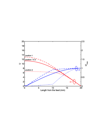
According to the results presented in Table 1, the most optimal location for the dielectric load in terms of the minimized radiation quality factor is position 1. It is seen in Fig. 3 that placing the substrate to position 1 leads to the highest voltage and current magnitudes along the patch. These higher magnitudes increase the stored energy, however, the higher radiation voltage (open-edge voltage) increases the radiated power. In this particular example this increase outweighs the effect of increased stored energy. When the substrate is placed to position 2, the voltage and current magnitudes are the lowest of all the considered cases. However, even though the amount of stored energy is the smallest, also the radiated power is small and the radiation quality factor is the highest of all considered cases.
| Analytical model | |||
| Position | (GHz) | ||
| 1 & 2 | 3.95 | 2.00 | 29.0 |
| 1 | 4.4 | 2.00 | 27.1 |
| 2 | 13.7 | 2.00 | 48.1 |
| Simulation results (IE3D) | |||
| Position | (GHz) | ||
| 1 & 2 | 3.7 | 1.99 | 27.95 |
| 1 | 4.2 | 2.00 | 26.72 |
| 2 | 12.5 | 2.00 | 38.79 |
Results in Table 1 also show that lower permittivity dielectrics are needed to retain the resonant frequency when the substrate is placed near the open edge where the electric response is the strongest.
3.2 Simulation results
In this section we simulate the antenna structure introduced above. The purpose is to validate the results given by the analytical model. We use a method of moments based simulation software IE3D. The ground plane is infinite in the simulation setup. To ensure that the radiation conductance is not affected by the substrate and corresponds as closely as possible to the analytical model we leave a 0.5 mm long empty section before the radiating edge. The antenna is fed with a narrow matching strip having length mm and width mm connected to a 50 probe.
The fractional impedance bandwidth and the unloaded quality factor can be calculated by representing the antenna as a parallel RLC circuit in the vicinity of the fundamental resonant frequency and using the input voltage standing wave ratio : [15]
| (24) |
Above, the coupling coefficient for a parallel resonant circuit is , where is the resonant resistance and is the characteristic impedance of the feed line. The voltage standing wave ratio is defined as:
| (25) |
We use a dB matching criterion to define the impedance bandwidth.
The simulation results are shown in Table 1. The simulation software gives quite accurately the same resonant frequencies for the three different cases with nearly the same material parameters as the analytical model.
When position 2 is filled with the substrate, the analytical model overestimates the required substrate permittivity, and thus, predicts a higher . The analytical model assumes that the shorting metal plate is perfectly conducting whereas the finite conductivity of metal is taken into account in the simulations. When the shorting plate has a certain effective impedance, the electric response near the plate would slightly increase due to a small increase in the electric field magnitude. This would lower the needed permittivity value.
3.3 Measured results
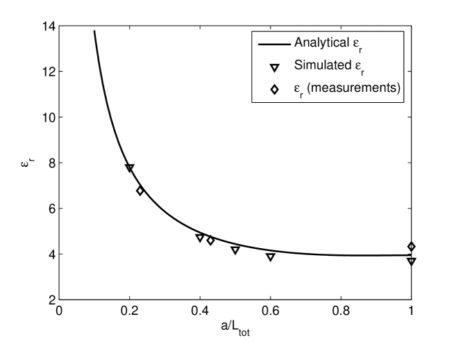
In this subsection we present some measurement results that further validate the analytical model. We have accurately replicated the antenna described in the previous sections. In the measurements the ground plane size is 3030 cm2, and we load different portions of position 1 with dielectric substrates having different permittivity values. The permittivity is altered from case to case in order to keep the resonant frequency fixed at 2 GHz. The loss tangent of the substrates is approximately 0.0027 in all cases.
The analytical value for is calculated using Eq. (11) and setting . The current amplitude at the open edge of our quarter wavelength antenna is zero at the resonant frequency. Knowing the resonant frequency ( GHz) and the permittivity of the material in position 2 (), can be solved using Eq. (11).
The measured impedance bandwidths (the unloaded quality factors) are shown in Fig. 4 and compared with the analytical results and simulated results. In the simulations the loss tangent is 0.001 in all cases. The corresponding permittivity values for each case are shown in Fig. 5. The measured quality factors and the corresponding permittivities agree well with the simulations and with the analytical model.
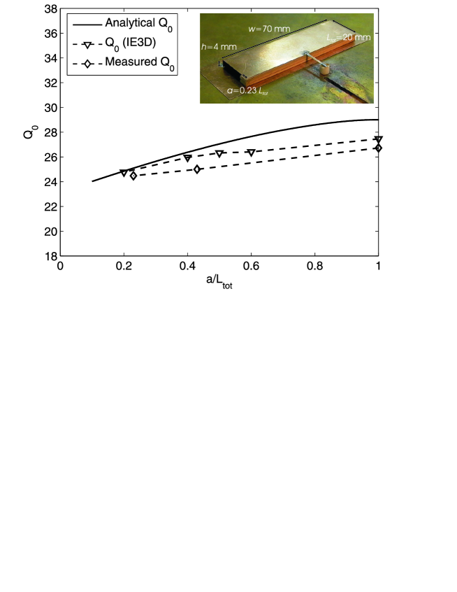
The difference in the results given by the analytical model and the measurements increase as the volume occupied by the substrate increases. This is expected since in the analytical model the corresponding increase in the dielectric losses is not taken into consideration.
3.4 Comparison with the results known from the literature
Let us compare the qualitative observations of our paper with the conclusions presented in [11]. In [11] the authors aim to broaden the impedance bandwidth of their example antenna by placing high permittivity dielectrics to the locations where the electric field magnitude is low, and low permittivity dielectrics where the electric field magnitude is strong. The aim is to create a more uniform field distribution in the antenna element. To demonstrate the feasibility of the method the authors first load a mm3 -patch antenna completely with a substrate having . In the second case portions of the substrate having length are replaced near the open edges by a substrate having . The reported resonant frequencies of the antennas are GHz and GHz. The authors compare qualitatively the impedance bandwidths and mention that partial filling is a feasible method to efficiently miniaturize microstrip antennas.
Here we will qualitatively replicate the comparison scheme of [11] using a mm3 -patch antenna. The antenna is divided into positions 1 and 2 as in Fig. 2. The length of position 1 is and the length of position 2 is . When the antenna volume is filled completely with a high-permittivity substrate having we get from the analytical model GHz and . Next we fill position 1 with a substrate having and use the high-permittivity substrate with in position 2. This leads to GHz and . We cannot, however, readily compare the quality factors as the two antennas operate at different frequencies. When comparing the impedance bandwidth properties of two antennas having the same volume and different resonant frequencies the proper figure-of-merit is as is seen from Eq. (23). Partial filling gives a higher value for this figure-of-merit, thus, the impedance bandwidth vs. size characteristics of the antenna are actually better in the case of uniform filling. If the resonant frequency of the partially filled antenna is brought to GHz we need to fill position 2 with a substrate having . This leads to . Since the two antennas operate now at the same frequency, we can directly compare the quality factors. Higher value for the partially filled case indicates that the filling scheme proposed in [11] is not optimal in terms of retained impedance bandwidth. As is shown in our paper, high-permittivity dielectrics need to be positioned to the locations where the electric field amplitude is the strongest.
The conclusion of paper [10] is that for effective size reduction a dielectric block should be positioned close to the radiating patch edges. This is in harmony with the conclusions from the above analysis.
4 Conclusions
We have derived the voltage and current distribution for a microstrip antenna loaded with two arbitrary dispersive and low-loss substrates. This model can be used to find the filling pattern that minimizes the antenna quality factor. We have presented an example miniaturization scheme where the antenna is partially filled with a conventional dielectric material blocks located in different positions under the antenna element. Qualitative design rules are given and the results of the analytical model are validated by numerical simulations and experiments. It has been shown that high-permittivity dielectrics need to be positioned to the locations where the electric field amplitude is the strongest in order to minimize the quality factor.
Acknowledgement
The authors wish to thank Prof. Constantin Simovski and Dr. Stanislav Maslovski for their valuable suggestions and advices.
References
- [1] I. J. Bahl and P. Bhartia, Microstrip antennas, Massachusettes: Artech House, 1980.
- [2] K. R. Carver and J. W. Mink, Microstrip antenna technology, IEEE Trans Antennas Propagat 1 (1981), pp. 2–24.
- [3] D. M. Pozar, Microstrip antennas, Proc IEEE 1 (1992), pp. 79–91.
- [4] C. A. Balanis, Antenna theory: Analysis and design, New York: John Wiley, 1997.
- [5] R. K. Mongia, A. Ittipiboon, M. Cuhaci, Low profile dielectric resonator antennas using a very high permittivity material, Electron Lett 17 (1994), pp. 1362–1363.
- [6] Y. Hwang, Y. P. Zhang, G. X. Zheng, T. K .C. Lo, Planar inverted F antenna loaded with high permittivity material, Electron Lett 20 (1995), pp. 1710–1712.
- [7] R. C. Hansen and M. Burke, Antennas with magneto-dielectrics, Microwave Opt Technol Lett 2 (2000), pp. 75–78.
- [8] S. A. Tretyakov, S. I. Maslovski, A. A. Sochava, C. R. Simovski, The influence of complex material coverings on the quality factor of simple radiating systems, IEEE Trans Antennas Propag 3 (2005), pp. 965–970.
- [9] P.M.T. Ikonen, S.I. Maslovski, C.R. Simovski, S.A Tretyakov, On artificial magnetodielectric loading for improving the impedance bandwidth properties of microstrip antennas, IEEE Trans Antennas Propagat 6 (2006), pp. 1654–1662.
- [10] B. Lee and F. J. Harackiewicz, Miniature microstrip antenna with a partially filled high-permittivity substrate, IEEE Trans Antennas Propagat 8 (2002), pp. 1160–1162.
- [11] C.-C. Chen and J. L. Volakis, Bandwidth broadening of patch antennas using nonuniform substrates, Microwave Opt Technol Lett 5 (2005), pp. 421–423.
- [12] R. E. Collin, Foundations for Microwave Engineering, 2nd Ed., New York: IEEE Press, 2001.
- [13] J. D. Jackson, Classical Electrodynamics, 3rd Ed., New York: John Wiley Sons, 1999.
- [14] J. S. McLean, A re-eximination of the fundamental limits on the radiation Q of the electrically small antennas, IEEE Trans Antennas Propagat 5 (1996), pp. 672–675.
- [15] H. F. Pues and A. R. Van de Capelle, An impedance-matching technique for increasing the bandwidth of microstrip antennas, IEEE Trans Antennas Propagat 11 (1989), pp. 1345–1354.