Scintillator counters with multi-pixel avalanche photodiode readout for the ND280 detector of the T2K experiment
Abstract
The Tokai–to–Kamioka (T2K) experiment is a second generation long baseline neutrino oscillation experiment which aims at a sensitive search for the appearance. The main design features of the T2K near neutrino detectors located at 280 m from the target are presented. Scintillator counters developed for the T2K near detectors are described. Readout of the counters is provided via WLS fibers embedded into S–shape grooves in a scintillator and viewed from both ends by multi–pixel avalanche photodiodes operating in a limited Geiger mode. A description, operational principles and the results of tests of photosensors with a sensitive area of 1.1 mm2 are presented. A time resolution of 1.5 ns, a spatial resolution of 9.9–12.4 cm, and a MIP detection efficiency of more than 99% were obtained for scintillator detectors in a beam test.
1 Introduction
The T2K project [1] is a second generation long baseline neutrino oscillation experiment which will use a high intensity off–axis neutrino beam produced by the JPARC 50 GeV (initially 40 GeV) proton beam. The first phase of the T2K experiment pursues two main goals: a sensitive measurement of and a more accurate determination of the parameters and than any previous experiment.
To achieve the physics goals, it is important to provide precise measurements of the neutrino beam properties, neutrino flux, spectrum and interaction cross sections. For these purposes, the near detector complex (ND280 [2]) will be built at the distance of 280 m from the target along the line between the average pion decay point and the Super-Kamiokande detector. In order to keep the systematics uncertainties below the statistical error, the physics requirements for ND280, discussed in detail in Ref. [2], can be briefly summarized as follows. The energy scale of the neutrino spectrum must be understood at the 2% level, and the neutrino flux should be monitored with better than 5% accuracy. The momentum resolution of muons from the charged current quasi–elastic interactions should be less than 10%, and the threshold for the detection of the recoil protons is required to be about 200 MeV/c. The fraction is to be measured with an uncertainty of better than 10%. The measurement of the neutrino beam direction with precision much better than 1 mrad is expected to be provided by the on–axis detector (neutrino monitor). The off–axis ND280 is shown in Fig. 1
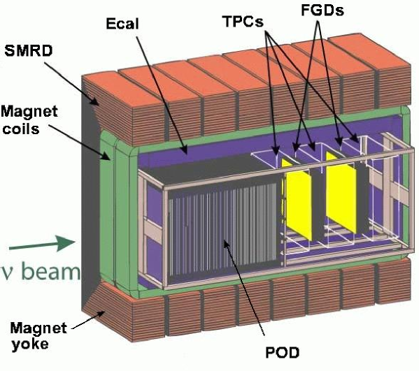
and consists of the UA1 magnet operated with a magnetic field of 0.2 T, a Pi-Zero detector (POD), a tracking detector which includes time projection chambers (TPC’s) and fine grained scintillator detectors (FGD’s), an electromagnetic calorimeter (Ecal), and a side muon range detector (SMRD).
The POD has been designed to be similar to the MINERA detector [3]. It is installed in the upstream end of the magnet and optimized for measurement of the inclusive production by on oxygen. The POD consists of 76 tracking planes composed of triangular polystyrene scintillating bars (about ) alternating with thin (0.6 mm) lead foils. Each bar has a 3 cm base, 1.5 cm height and a central hole for a WLS fiber. Three TPC’s will measure the 3–momenta of muons produced by charged current interactions in the detector and will provide the most accurate measurements of the neutrino energy spectrum. The ND280 will contain two FGD’s, each with dimensions m3 resulting in a total target mass of 1.2 tons. The first FGD will be an active scintillator detector, similar to the SciBar [4] detector of the K2K experiment [5]. Each FGD layer will consist of 200 scintillator bars, and thirty layers will be arranged in alternating vertical and horizontal layers perpendicular to the beam direction. The second FGD will consists of layers scintillator bars alternating with 3 cm thick layers of passive water. The Ecal surrounds the POD and tracking region and consists of 15 layers, each of which has one sheet of 3 mm Pb alloy and one layer of 1 cm thick 5 cm wide plastic scintillator bars (with signal readout by WLS fibers). Interior to this section is the preradiator section, where each of the 3 layers consists of a lead alloy sheet backed by 3 layers of scintillator bars. Air gaps in the UA1 magnet will be instrumented with plastic scintillator to measure the ranges of muons which escape at large angles with respect to the neutrino beam and which can not be measured by the TPC’s. The active component of the SMRD will use scintillators with wavelength shifting fibers (WLS) readout to transport the light into photosensors.
The ND280 detector will widely use WLS fiber readout with light detection from fibers by photosensors which have to operate in a magnetic field environment and limited space inside the UA1 magnet. The primary candidate for the photosensor is the multi–pixel avalanche photo-diode operating in the limited Geiger multiplication mode [6, 8, 9, 10]. Such photodiodes are compact, well matched to spectral emission of WLS fibers, and insensitive to magnetic fields [11, 12].
2 Geiger mode multi–pixel avalanche photodiodes
2.1 Overview
The multi-pixel avalanche photodiodes with a metal–resistor–semiconductor layer structure operating in the limited Geiger mode (hereafter referred to as MRS APD’s or MRS photodiodes) are invented and designed by the Center of Perspective Technologies and Apparatus (CPTA), Moscow [6]. Detailed description of these devices and principles of operation can be found in Refs. [7, 9, 13]. Such a photosensor consists of many pixels on a common p–type silicon substrate. A simplified topology of a MRS photodiode is shown in Fig. 2.
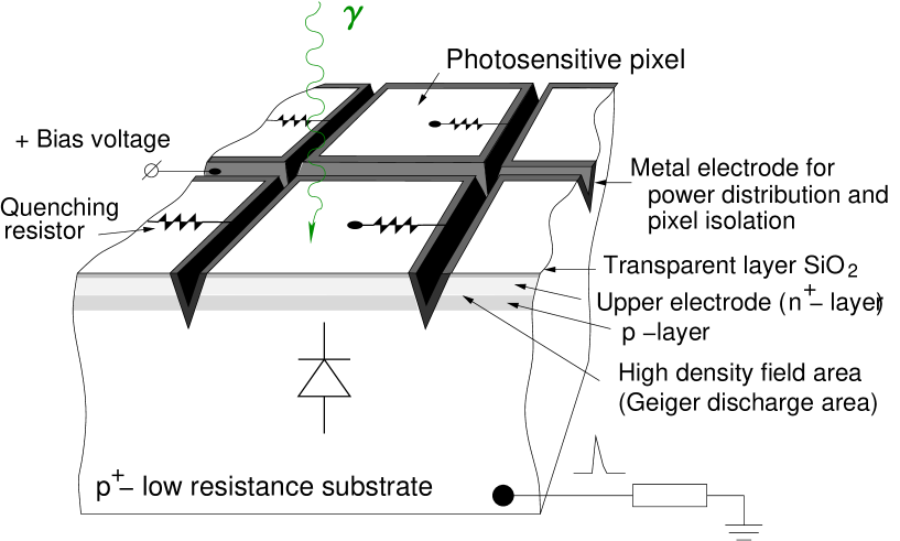
Each pixel operates as an independent Geiger micro-counter with a gain of the same order as a vacuum photomultiplier. Geiger discharge is initiated by a photoelectron in the high electric field created in a very thin layer of about 1 m by the applied bias voltage. The discharge current for each pixel produces a voltage drop at individual resistors. As a result, the electric field density becomes small and can no longer support the discharge quenched in such a way. Small pixels are separated by grooves filled with an optically non–transparent material to suppress the cross–talks. The gain is determined by the charge accumulated in a pixel capacitance: , where is difference between the bias voltage and the breakdown voltage of the diode (overvoltage). Since is about a few volts and fF, then typical fC, that corresponds to electrons. A single incident photon can fire more than one pixel. Thus, the gain of the MRS photodiode is equal to the charge of a pixel multiplied by the average number of pixels fired by a single photon.
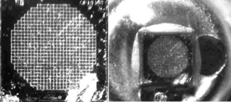
The amplitude of a single pixel signal does not depend on the triggered number of carriers in this pixel. In such a way, the photodiode signal is a sum of fired pixels. Each pixel operates as a binary device, but the multi–pixel photodiode as a whole unit is an analogue detector with a dynamic range limited by the finite number of pixels. The pixel size can be to m2, and the total number of pixels is 100–4000 per mm2. We tested the CPTA MRS photodiodes with a sensitive area of 1.1 mm2 with 556 pixels of size (see Fig. 3).
2.2 Basic properties of the CPTA MRS photodiodes
The main parameters of the MRS photodiodes such as the gain, photon detection efficiency, intrinsic noise, cross–talk, depend on the applied bias voltage. The MRS photodiodes were tested using a signal from a green light emitting diode (LED). The MRS signal was amplified and split into two signals: one was fed to a discriminator, another was measured by an ADC with a gate of about 100 ns.
Gain. A typical operating voltage is around 40 V for the tested MRS photodiodes, although the voltage can differ by a few volts to provide the same gain in photodiodes. The MRS photodiode has an excellent single photoelectron (p.e.) resolution determined mainly by electronics noise even at room temperature. It means that there is only a small pixel to pixel gain variation as well as small fluctuations in Geiger discharge development. The absolute gain depends on the photodiode topology, bias voltage and temperature. The voltage and temperature sensitivities of the MRS photodiode gain are rather weak as will be demonstrated below. A 0.1 V change in bias voltage corresponds to a 2–3% variation in gain. The charge of a single p.e. signal in a calibrated ADC was used to determine the MRS photodiode gain. The typical gain value at room temperature (22∘C) is obtained to be about .
Photon detection efficiency. The photon detection efficiency (PDE) of a multi-pixel avalanche photodiode operating in the limited Geiger mode is a product of 3 factors:
| (1) |
where is the wavelength dependent quantum efficiency, is the probability for a photoelectron to initiate the Geiger discharge, is a fraction of the total photodiode area occupied by sensitive pixels. The bias voltage affects one parameter in expression (1) . The geometrical factor is completely determined by the MRS photodiode topology. Its value is estimated to be about 70–80% in an ideal case. The absolute value of the PDE was measured using small pulses from a green LED (525 nm) which illuminated a MRS photodiode through a 0.5 mm diameter collimator. The number of emitted photons was obtained using a calibrated PMT XP2020. The normalized PDE values at 525 nm for different bias voltages are presented in Fig. 4.
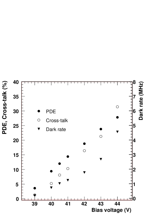
The cross-talk contribution was subtracted from the signal to obtain the correct value of the PDE, the accuracy of which is estimated to be about 20%. As seen in Fig. 4, the PDE is about 12% at a dark rate of 1 MHz. The PDE can be increased up to almost 30% at the expense of much higher dark rate.
The PDE dependence on the wavelength of the detected light, as well as the emission spectrum of the WLS fiber Y11 are shown in Fig. 5.
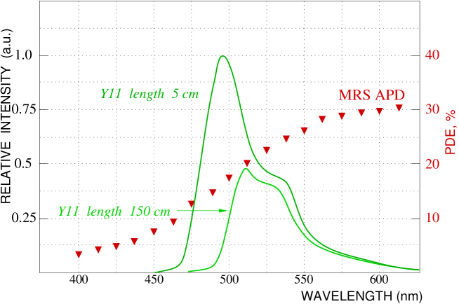
The peak emission of the fiber depends on its length due to the absorption of the light. The spectral response of a MRS photodiode was measured in a spectrophotometer calibrated with a PIN–diode [15]. The PDE was measured at higher and, therefore, the dark rate was higher (about 2.3 MHz for a discriminator threshold of 0.5 p.e.). The PDE decreases by about 50% when is lowered such that the dark rate is MHz.
Dark rate. The limiting factor for a wide application of the MRS photodiodes in the readout of scintillators is the dark noise rate which originates from thermally created carriers in the depletion region under high electric fields. The dark rate mainly consists of single p.e. pulses. Larger amplitude pulses also contribute to the dark rate, as shown in Fig. 6.

However, the intensity of the pulses with 2 p.e. amplitudes is about 15 times less than the intensity of the single p.e. pulses. Large amplitudes ( p.e.) are generated by the optical cross-talk as well as by accidental pile-ups between the independent pixels, though the second effect is relatively small. The dark rate decreases to the level of a few kHz for the threshold of 2.5 p.e. The intensity of 1 p.e. pulses as well as 2 p.e. pulses is significantly higher for higher bias voltage, as can be seen from Fig. 6 in case of V. Dark pulses and mostly leakages create the dark current through a MRS photodiode in a typical range of . The dark rate decreases to about 1 kHz/mm2 at C, i.e. decreases by a factor of 2 for every temperature drop of C for a threshold of 0.5 p.e. and and the condition of keeping the gain at a constant value by tuning the bias voltage.
Optical cross–talk. A single incident photon can create more than a single p.e. due to optical cross–talk. The mechanism of this effect is not quite clear. Models predict that during the Geiger discharge and recombination of carriers infrared photons are emitted. These photons penetrate into the adjacent pixels and fire them. Optical cross–talk leads to a higher than expected signal as Geiger discharge occur in additional pixels. The absolute value of the cross–talk can be calculated by assuming a Poisson distribution for the number of photoelectrons observed in response to the light from a LED. When the MRS photodiode noise is small, the measured mean number of fired pixels by the LED photons, , is compared with the calculated value given by
| (2) |
where is the fraction of 0 p.e., or “pedestal” events. Then the deviation of the ratio from 1 gives the cross–talk value. These values are presented for several bias voltages in Fig. 4. A cross–talk value of about 5% was obtained at a bias voltage that provides a dark noise rate of MHz at a discriminator threshold of 0.5 p.e. The cross–talk is larger for higher bias voltage. The sharp decrease of the dark rate shown in Fig. 6 is a good demonstration of the low optical cross–talk. It should be noted that the signal amplitude in photoelectrons is less than the measured amplitude determined as the average number of fired pixels by the cross-talk value, i.e. by a few per cent.
Temperature dependence. The PDE and gain of MRS photodiodes (as well as the signal amplitude) are expected to be sensitive to temperature because the breakdown voltage depends on temperature. The MRS signal amplitude (light yield) is proportional to , where is the number of photons from the LED which illuminate the photodiode. The parameters of the MRS photodiodes were measured over temperatures from 15∘ to 33∘C. The temperature variation of the MRS signal (a green LED was used as a light source) is presented in Fig. 7.
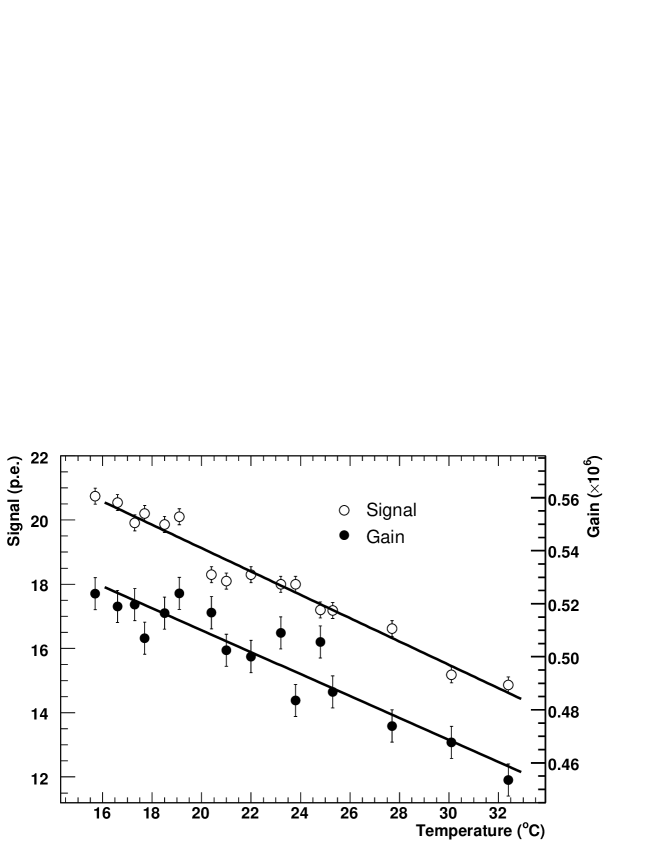
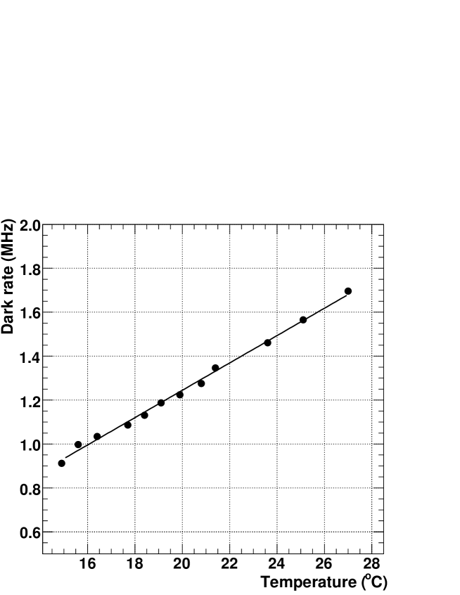
The MRS signal dependency of -1.5 %/∘C is obtained for increasing temperature. The MRS gain itself decreases with temperature as -1.2 %/∘C (see Fig. 7), while the PDE varies with temperature as -0.3 %/∘C. The dark rate depends on temperature with a coefficient of 62 kHz/∘C, as shown in Fig. 8.
Decreasing the temperature below C greatly reduces the noise and increases the PDE, as shown in Ref. [15].
Recovery time. The ability of MRS photodiodes to operate at high counting rates was tested using two LED signals. We measured the amplitude of the second signal as a function of the time difference between the first and second signal. Fig. 9 shows the ratio , where is the amplitude of the second signal when the first LED signal is off.
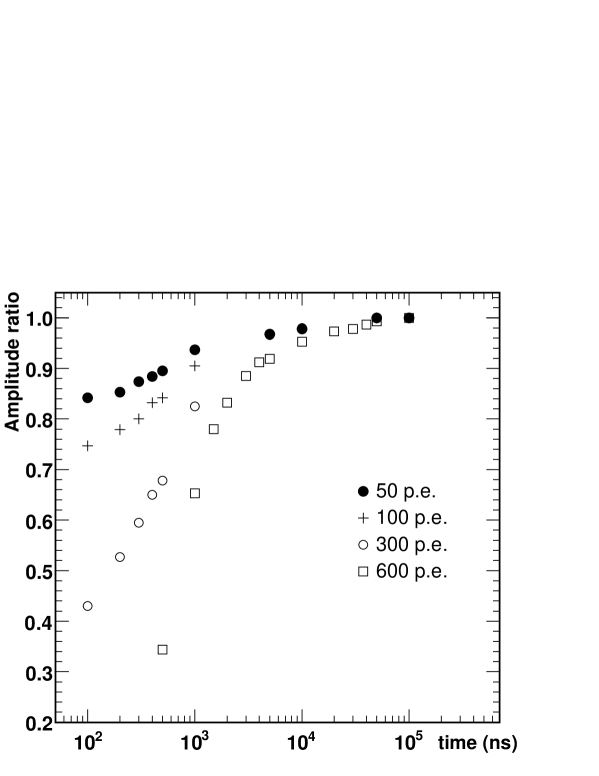
As seen from Figure 9, a minimum time interval between the first and second pulse of about 5 s is needed to recover about 95% of the full amplitude of the second signal. This long recovery time is due to the fact that the individual resistor of each pixel, , has the value of about 20 M, the pixel capacitance is typically 50 fF that gives s.
Dynamic range and linearity. The dynamic range of the MRS photodiode is limited by the finite number of pixels. The saturation of the MRS photodiode in response to large light signals is shown in Fig. 10.
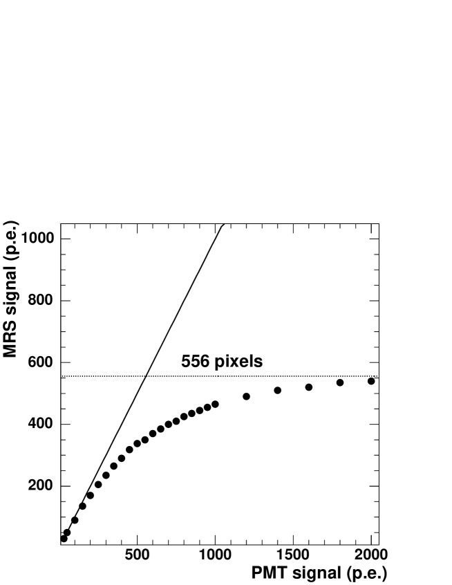
In this test, the LED signal was ajusted to obtain similar response for both PMT and MRS photodiode at the light yield below 150 p.e. The photodiode signal is linear for low amplitutes. A nonlinearity of about 10% is already seen for a signal of 150–200 p.e. For the PMT signal of 500 p.e., the MRS photodiode has a 30% smaller signal than that of the PMT. Full saturation of the 556 pixel MRS photodiode starts at a reference (PMT) signal of more than 2000 p.e.
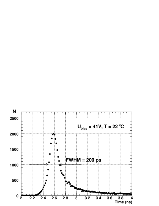
Timing. The development of the Geiger discharge in a small depth () of the depletion region takes a few hundred picoseconds. The typical rise time is 1 ns, the decay time is determined by the pixel capacitance. A laser with a wavelength of 635 nm and a pulse width of 35 ps (fwhm) was used to measure the intrinsic time resolution of 1 p.e. pulses. Very weak laser light created only 1 p.e. signals in a MRS photodiode. The time resolution obtained for a threshold of 0.2 p.e. at C is presented in Fig. 11.
Life time. The failure rate of the MRS photodiodes is an important figure of merit for the overall detector performance, because most photodiodes can not be replaced without significant disassembly of the ND280 detector. Exposures to elevated temperature are used to evaluate the expected life time of semiconductor devices. We have placed 19 MRS photodiodes in an oven at 80∘C for 30 days. All photodiodes were kept under bias voltages to provide the same dark current as at room temperature. One of the devices started to conduct a large current after a week of heating. The failed device had the worst PDE among of the tested devices. This points to a possible defect in its structure. All other devices passed the test without residual effects, and the LED signals measured by these MRS diodes after a period of 30 days of elevated temperatures did not show any significant degradation. The signals of the tested photodiodes in response to a LED photons were measured before the heating and for a period of about 260 days after the heating. The results for two devices are presented in Fig. 12.
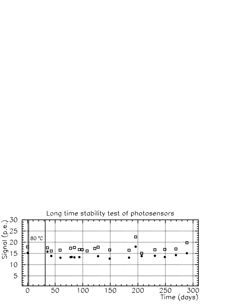
The accuracy of the l.y. measurements is about 2.0 p.e. (rms) due to misalignments between the fiber and the MRS photodiodes that are estimated to be between 20 and 100 m in this series of tests. For more than 7 months after heating no degradation in the light yield was observed.
Two hundred MRS photodiodes fabricated from a few different wafers were tested. In order to meet the requirements of the experiment, the dark rate of each device should be kept close to a reference value of 1 MHz at room temperature 22∘C and for a discriminator threshold of 0.5 p.e. This required the individual adjustment of the bias voltage of 38 to 42.1 V for each photodiode, that in turn resulted in a wide range of 8.9–18.8% for the PDE values, and the gains of these 200 MRS photodiodes were found to be between and .
3 Scintillator detectors with WLS fiber readout
Several subdetectors of the T2K near detector complex will be composed of many scintillator detectors: rectangular and triangular scintillator bars, and various scintillating slabs. All these elements use embedded WLS fibers to read light from the scintillators. A well known design will be adopted for the bars with WLS fibers: one straight hole or groove on one surface for a WLS fiber. For large scintillator slabs (SMRD, active elements of Ecal), the usage of the standard readout scheme with several equidistant WLS fibers which run along the slab is not appropriate due to mechanical constraints of the UA1 magnet. We consider extruded scintillator slabs with a double–ended WLS fiber readout technique as active elements for the SMRD detector. Instead of a few parallel WLS fibers we propose to use a single long WLS fiber embedded in an S–shape groove which reduces the maximum path length that light has to travel within the scintillator to a few cm. The detector prototypes were manufactured using an extrusion technique developed at the Uniplast Factory, Vladimir, Russia. The scintillator is etched by a chemical agent that results in the formation of a micropore deposit over the plastic surface. The thickness of the deposit (30–100 m) depends on the etching time. Details can be found in Ref. [16]. A scintillator slab of 1x17x87 cm3 with an S–shaped groove of 3 mm depth was manufactured for a test in a pion/proton beam. The half–period of the S–shape groove is 58 mm, as shown in Fig. 13.
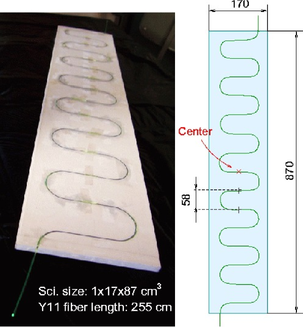
A 2.55 m long multi–clad Kuraray Y11 (200 ppm dopant) WLS fiber of 1 mm diameter is embedded into the groove with an optical grease and both ends are attached to MRS photodiodes. To avoid the degradation of the Y11 parameters in real SMRD counters, the bending procedure to make 3 cm radius loops will be done at the temperature of about 80∘C.
This module was first tested with cosmic muons. A light yield (l.y.) of 16.4 p.e. was obtained for MIP’s in the center for summed signals from both photodiodes. In order to suppress the timing spread caused by the trigger counters the combination was used to measure the time resolution. A time resolution of ns was obtained for MIP’s which passed through the central part of the slab.
4 Beam tests of the SMRD prototype
4.1 Beam test setup
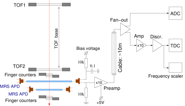
A beam test of extruded scintillators with embedded WLS fibers was performed at the KEK 12-GeV proton synchrotron with 1.4 GeV/c protons and pions. Two counters were placed in a beam and tested simultaneously. One was the S–grooved scintillator (S–counter) described in the previous section, another one was a scintillator slab, 1x18x50 cm3 in size, with a single straight groove in the middle of the plastic (W–counter). An 1.11 m long Kuraray Y11(200) fiber of 1 mm diameter was embedded with optical grease into the straight groove of the W–counter. The fiber in each counter is viewed from both ends by MRS photodiodes. The fibers are directly coupled to photosensors inside special sockets. The detectors were mounted on a platform which could be moved horizontally and vertically with respect to the beam line. Upstream of the counters, a TOF system was used to separate pions and protons. Finger trigger counters restricted the beam spot size to a square. The signals were amplified by fast hybrid preamps mounted directly behind the photodiodes. The bias voltage was set individually for each MRS photodiode to limit the dark rate to about 1.2 MHz for a 0.5 p.e. threshold. A simplified electronic diagram of the beam test setup is shown in Fig. 14.
Only pions were selected for analysis as their response is close to that expected from MIP’s in the T2K experiment. The ambient temperature drifted between 15–18∘C during the beam test. Typical ADC spectra from pions are shown in Fig. 15.
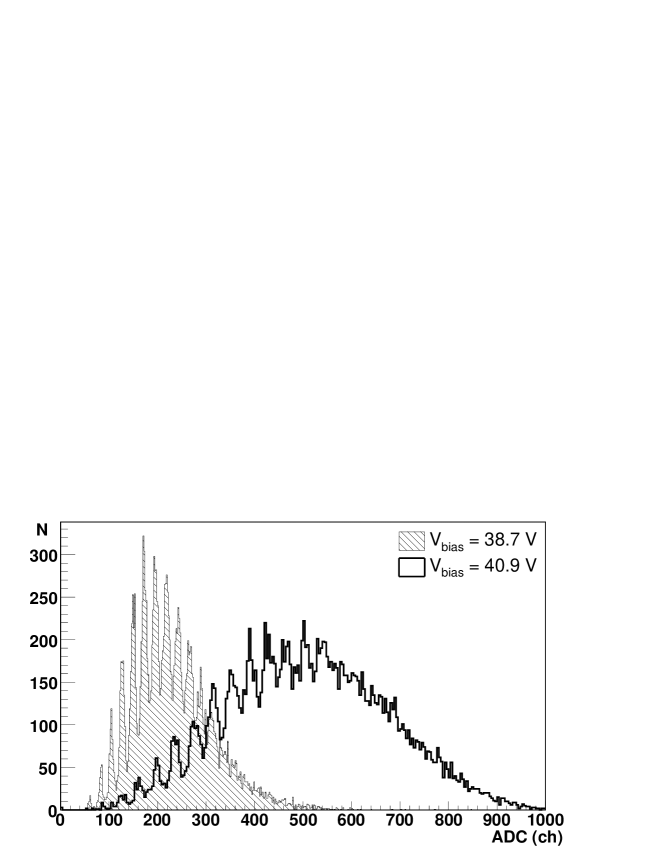
In this Figure, one spectrum is obtained with a bias voltage of 38.7 V which corresponds to a dark rate of 0.86 MHz for a discriminator threshold of 0.5 p.e. The second spectrum is measured with a bias voltage of 40.9 V corresponding to a dark rate of almost 2 MHz. The individual photoelectron peaks are clearly separated at 38.7 V and still visible at 40.9 V.
4.2 Detection efficiency of MIP’s
The light yield scan over the S–counter surface is presented in Table 1.
| , mm | -80 | -60 | -40 | -20 | 0 | 20 | 40 | 60 | 80 |
| , mm | |||||||||
| -406 | 6.3 | 11.9 | 13.2 | 16.0 | 17.8 | 18.6 | 18.7 | 18.8 | 13.8 |
| -319 | 10.2 | 11.6 | 14.7 | 15.7 | 15.9 | 16.4 | 17.3 | 16.7 | 13.2 |
| -200 | 10.2 | 12.7 | 14.3 | 16.0 | 15.5 | 16.6 | 18.2 | 18.7 | 15.0 |
| -87 | 10.4 | 11.7 | 13.0 | 15.0 | 15.0 | 15.4 | 16.3 | 14.5 | 11.0 |
| -30 | 8.8 | 14.4 | 16.4 | 16.2 | 15.3 | 14.6 | 13.8 | 12.9 | 10.9 |
| 0 | 11.0 | 12.9 | 14.8 | 14.3 | 15.3 | 16.2 | 14.9 | 13.9 | 11.7 |
| 30 | 9.3 | 11.8 | 12.6 | 14.4 | 14.8 | 15.8 | 16.8 | 16.0 | 13.0 |
| 87 | 12.3 | 14.4 | 15.1 | 14.6 | 14.2 | 14.7 | 14.2 | 12.9 | 11.8 |
| 200 | 11.0 | 15.2 | 16.0 | 15.9 | 15.6 | 15.5 | 13.7 | 12.9 | 11.3 |
| 319 | 12.6 | 16.1 | 17.4 | 16.3 | 15.5 | 15.2 | 14.5 | 12.3 | 10.4 |
| 406 | 11.8 | 12.9 | 17.9 | 19.9 | 20.0 | 19.1 | 19.1 | 16.2 | 11.9 |
The beam spot spreads beyond the scintillator area near the edges at mm causing the small l.y. values. If the edges are ignored, the light output over the S–counter (sum of both end signals) varies from 12 to 20 p.e./MIP. The largest l.y. is measured at the ends, close to either of the two MRS photodiodes. In order to obtain the detection efficiency the ADC spectra were analyzed. The event is considered accepted if its ADC amplitude exceeds a certain threshold set in number of p.e. The average statistics in each location is about 2000 events. Table 2
| , mm | -80 | -60 | -40 | -20 | 0 | 20 | 40 | 60 | 80 |
| , mm | |||||||||
| -406 | 0.660 | 0.995 | 0.999 | 1.000 | 1.000 | 0.999 | 1.000 | 1.000 | 0.999 |
| -319 | 0.750 | 0.999 | 0.999 | 0.999 | 0.999 | 0.999 | 0.999 | 0.998 | 1.000 |
| -200 | 0.788 | 0.998 | 0.999 | 0.999 | 1.000 | 1.000 | 0.999 | 0.999 | 1.000 |
| -87 | 0.839 | 0.996 | 0.998 | 0.999 | 1.000 | 0.999 | 1.000 | 0.999 | 0.995 |
| -30 | 0.886 | 0.999 | 0.999 | 1.000 | 1.000 | 0.999 | 1.000 | 0.997 | 0.998 |
| 0 | 0.985 | 0.998 | 0.997 | 0.998 | 0.996 | 0.998 | 0.999 | 0.999 | 0.998 |
| 30 | 0.918 | 0.996 | 0.998 | 0.999 | 1.000 | 1.000 | 1.000 | 0.999 | 0.998 |
| 87 | 0.989 | 0.997 | 1.000 | 0.999 | 0.999 | 1.000 | 0.998 | 0.999 | 0.996 |
| 200 | 0.995 | 0.998 | 1.000 | 0.999 | 1.000 | 1.000 | 1.000 | 0.999 | 0.994 |
| 319 | 0.999 | 0.998 | 1.000 | 1.000 | 1.000 | 1.000 | 1.000 | 0.998 | 0.994 |
| 406 | 0.998 | 0.999 | 1.000 | 1.000 | 1.000 | 0.999 | 1.000 | 1.000 | 0.984 |
demonstrates the S–counter pion detection efficiency when the threshold for the sum of both end signals is set to 2.5 p.e. The detection efficiency is close to 100 % except for the edge area where a part of the beam missed the counter due to some misalignment between the beam counters and the tested detector. For a higher threshold of 4.5 p.e set for the sum of the amplitudes from the two ends, the MIP detection efficiency is greater than 98%. We can conclude that the l.y. of more than 12 p.e. (sum of both ends) satisfies the requirement for the S–counter to provide a detection efficiency greater than 99% for a MIP. If we require that each MRS photodiode signal exceeds 0.5 p.e. the MIP detection efficiency is found to be about 99.5%.
To make a detailed scan along the middle line of the S–counter the size of the beam spot was reduced to cm2. The result is shown in Fig. 16.
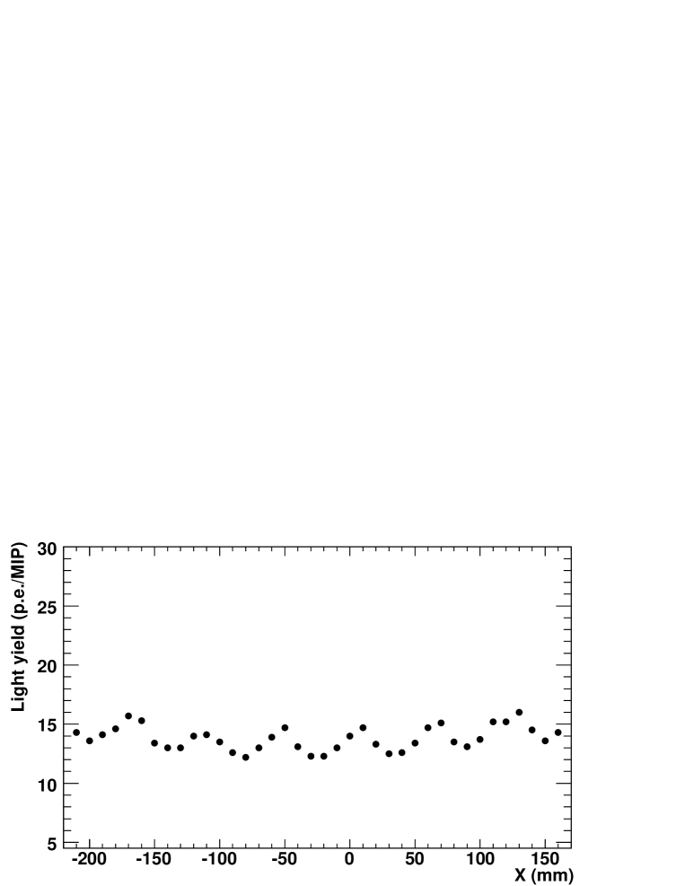
The WLS fiber route is clearly reflected in the pattern of the l.y. distribution along the x–axis. A maximum l.y. is observed in points where the beam crosses the fiber, while the l.y. drops by about 20% in between the fiber segments. Fig. 17
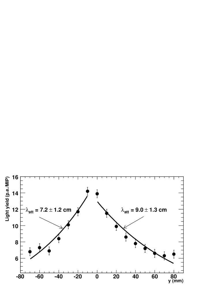
shows the result of the transverse l.y. scan across the W–counter, which has a single straight groove running down the middle of the counter. The attenuation length of scintillation light before capture by the WLS fiber is obtained to be cm and cm for the upper and the lower part of the W–counter, respectively. These values are consistent within measurement uncertainty, and the average attenuation length of such a counter is estimated to be about cm.
4.3 Time and spatial resolution of the S–counter
The time resolution was measured with the discriminator thresholds set to a level of 0.5 p.e. for each MRS photodiode. To suppress the timing spread caused by the trigger counters (as in the cosmic ray test) we used the combination to determine the time resolution. The dependence of the time resolution on the light yield is presented in Fig. 18.
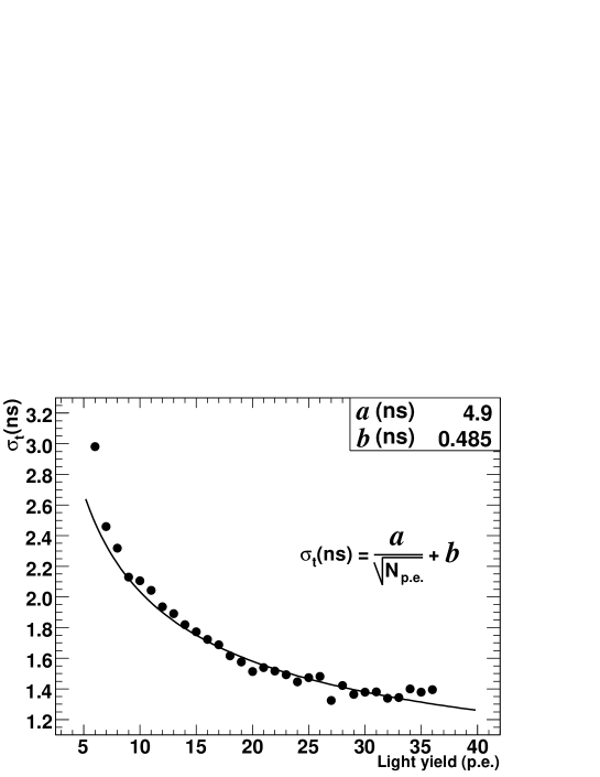
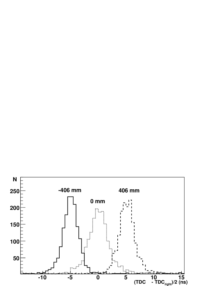
The time resolution depends on photostatistics and is proportional to . At a typical l.y. of 15 p.e./MIP ns is obtained. The time resolution of the S–counter is mainly determined by the slow decay time of the Y11 fiber. Green light travels along a WLS fiber at a speed of 17 cm/ns while the signal propagates along the counter at a smaller speed of 7.4 cm/ns because of the fiber routing. The time spectra for 3 positions of the beam along the S–counter are shown in Fig. 19.
The obtained time difference between left and right signals allows us to extract the beam coordinate along the S–counter using the expression
| (3) |
A spatial resolution of cm is obtained in the center of the S–counter and cm near both ends.
The spatial resolution can be improved taking into account the light attenuation along the fiber. The asymmetry between the signals from the left and right MRS photodiodes is sensitive to the hit position of a MIP, but the spatial resolution obtained using the l.y. attenuation is poor ( cm) because of large fluctuations in the light yields. However, the combination of both methods
| (4) |
where and are the MIP positions obtained from timing and amplitude asymmetry with accuracies of and , respectively. The weight is given by , allows us to slightly improve the spatial resolution. Fig. 20
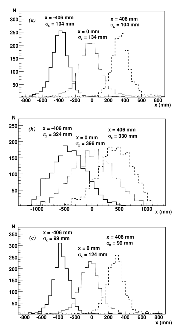
shows the spatial resolution for three beam positions obtained for the combination of the signal timing and amplitude. The spatial resolution in the center of the S–counter is obtained to be 12.4 cm, while it is about 9.9 cm at both ends.
5 Conclusion
The scintillator counters for the SMRD of the T2K near detector have been designed and tested. The readout of the extruded scintillator counters is provided via a WLS fiber which is embedded into an S–shape groove and viewed from both ends by multi–pixel avalanche photodiodes operating in the limited Geiger mode. The studied MRS photodiodes demonstrate good performance: a low cross-talk of a few per cent, the photon detection efficiency for green light of about 12%, and a long term stability. These devices are insensitive to magnetic fields, their calibration and stability control can be provided by means of the excellent p.e. peak resolution. The linearity range of the tested MRS photodiodes is less than 200 p.e. and the recovery time is about 5 s. Although these parameters might be critical for some applications, this performance is acceptable for many detectors of the ND280 complex of the T2K experiment.
An average l.y. of about 15 p.e./MIP, a MIP detection efficiency greater than 99.5%, a time resolution of 1.75 ns for a MIP, and a spatial resolution of cm were obtained in a pion beam test.
The authors are grateful to D. Renker, A. Akindinov and A. Konaka for useful discussions. This work was supported in part by the “Neutrino Physics” Programme of the Russian Academy of Sciences.
References
- [1] Y. Itow et al., hep-ex/0106019.
- [2] “T2K ND280 Conceptual Design Report”, T2K Internal Document.
- [3] D. Drakoulakos et al., hep-ex/0405002.
- [4] K. Nitta et al., Nucl. Instr. Meth. A535 (2004) 147; S. Yamamoto et al., IEEE Trans. Nucl. Sci. 52 (2005) 2992.
- [5] E. Aliu et al., K2K Collaboration, Phys. Rev. Lett. 94, 081802 (2005); S. Yamamoto et al., K2K Collaboration, Phys. Rev. Lett. 96, 181801 (2006).
- [6] G. Bondarenko, V. Golovin, M. Tarasov, Patent for invention in Russia No. 2142175, 1999.
- [7] V. Golovin et.al., Patent for invention in Russia, No. 1644708, 1989; A.G. Gasanov et al., Lett. J. Techn. Phys. 16 (1990) 14 (in Russian).
- [8] Z.Ya. Sadygov et al., Nucl. Instr. Meth. A504 (2003) 301.
- [9] G. Bondarenko et al., Nucl. Instr. Meth., A442 (2000) 187.
- [10] P. Buzhan et al., Nucl. Instr. Meth. A504 (2003) 48.
- [11] V. Andreev et al., Nucl. Instr. Meth., A540 (2005) 368.
- [12] D. Beznosko et al., FERMILAB-PUB-05-410.
- [13] A. Akindinov et al., Nucl. Instr. Meth. A387 (1997) 231.
- [14] Kuraray Co., Ltd., Scintillator Fiber Products, 1994.
- [15] E. Gushchin et al., ”Multi-pixel Geiger-mode avalanche photodiodes with high quantum efficiency and low excess noise factor”, Proceedings of the 4th Int. Conf. on New Developments in Photodetection, Beaune, 2005, to be published in NIM.
- [16] Yu.G. Kudenko et al., Nucl. Instr. Meth. A469 (2001) 340; O. Mineev et al., Nucl. Instr. Meth. A494 (2002) 362; N. Yershov et al., Nucl. Instr. Meth. A543 (2005) 454.