Plasmonic bandgaps and Trapped Plasmons on Nanostructured Metal Surfaces
Abstract
Nanostructured metal surfaces comprised of periodically arranged spherical voids are grown by electrochemical deposition through a self-assembled template. Detailed measurements of the angle- and orientation-dependent reflectivity reveal the spectral dispersion, from which we identify the presence of both delocalized Bragg- and localized Mie-plasmons. These couple strongly producing bonding and anti-bonding mixed plasmons with anomalous dispersion properties. Appropriate plasmon engineering of the void morphology selects the plasmon spatial and spectral positions, allowing these plasmonic crystal films to be optimised for a wide range of sensing applications.
pacs:
73.20.Mf, 42.70.Qs, 72.15.Rn, 81.07.-bIn recent years the topic of surface plasmons and plasmon-active surfaces has become of interest to a broad range of disciplines.Barnes03 Stemming from the desire to construct plasmon devices and the ability to make and characterize metallic structures on the nano-scale, plasmonics finds applications in fields as diverse as optical switchingKrasavin05 , near-field photonicsZayats03 and surface-enhanced Raman spectroscopy.Tian02 A critical issue for the application of plasmons is their location and spatial extent within complicated 3D metal geometries. Despite impressive progress in the field of scanning near-field microscopy, the technique is selective in the plasmons it records, is somewhat invasive to the plasmon fields, and is unable to distinguish between localized or delocalized modes.Hohng02 The difficulties are exemplified by the extended debate about how light squeezes through arrays of sub-wavelength holesEbbesen98 . Similarly, extreme localization of plasmons on rough metal surfaces is thought to produce ‘hot-spots’ for resonant Raman scattering.Stockman01 It has, however, proved difficult to study in detail this process of plasmon localization.
Here we study the band-structure of, and coupling between different plasmon modes on a series of carefully controlled metal nanostructured surfaces. By measuring the polarized reflectivity of a focused white light laser while varying the sample orientation and incident angle, the spectral dispersion of surface and localized plasmons as a function of sample geometry is measured. Strong coupling between different plasmon modes is clearly observed, along with the systematic localization of surface plasmons at a critical geometrical condition. Understanding the complexity of the plasmon localization opens the way to plasmon engineered surfaces, designed for particular applications.
Along the boundary between a metal and a dielectric, surface plasmon-polaritons (SPPs) can propagate freely. By patterning such surfaces with a periodic array of holes, an incident optical field can be diffracted and couple to these SPPs.Hooper02 The SPPs will also multiply scatter off the periodic components of the array leading to ‘Bragg’ plasmon modes with plasmonic bandgaps. Plasmons can become localised if the field fluctuations become spatially pinned and disconnected from each other. These localised modes are highly dependent on the geometry of the surface and have attracted a growing interest for achieving large field enhancements.Bergman03
The nano-structured surfaces investigated here are formed using a nano-casting process, by electrochemical deposition through a template of self-assembled latex spheres.Bartlett00 ; Bartlett03 The resulting metallic mesh reflects the order of the self-assembled close-packed template, allowing convenient control of the pore diameters and regularity of the array. Templates are produced using a capillary force method, allowing a monolayer of well-ordered spheres to be produced, with sphere diameters, , (and hence pitch) between 100nm and m. Electro-deposition while measuring the total charge passed allows the accurate growth of metal to a required thickness . Furthermore by systematically retracting the sample from the plating bath during growth, the nano-structure geometry can be graded. After deposition the template is dissolved, leaving the freestanding structure. This allows the production of shallow well-spaced dishes as well as encapsulated spherical voids on a single sample. Optical and electron microscopy shows that the resulting surfaces are smooth on the sub-10nm scale. We combine these with scanning probe microscopy to determine the film thickness locally. Here we concentrate mostly on Au voids, although very similar features are seen for Ag samples.
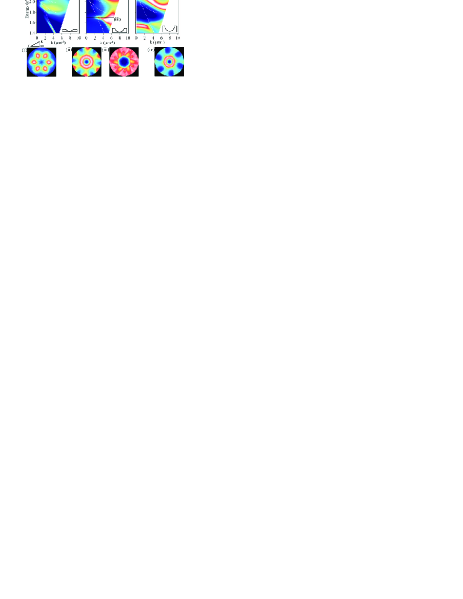
On thin regions of the sample (normalised film thickness, ) where the surface takes the form of a hexagonal array of shallow dishes, SPPs are observed. These states multiply scatter off the rims of the dishes, forming plasmonic bandgaps similar to those formed in 2D dielectric photonic crystals. For weak scattering these Bragg plasmons track the folded plasmon dispersion in the 2D lattice (Fig.1a). The Bragg scattering mixes these six-fold degenerate modes, splitting their energies and forming travelling Bloch waves with different standing wave field distributions within each unit cell (bands 1,2,6 shown for small in-plane along the direction)Joannopoulos95 . These distributions are calculated in a weak 2D dielectric photonic crystal approximation, and show markedly different overlap with the circular holes. Because the Bragg plasmons are travelling Bloch modes, their energy depends strongly on their direction of propagation.Satpathy90 As the thickness of the film increases, the rim of the spherical voids expands while the pitch remains constant, strongly increasing the scattering of the Bragg plasmons. For hemispherical voids, the top planar surface breaks up into disconnected triangular islands, preventing straightforward passage of the surface modes.

On the other hand, localized plasmons are trapped in the deep spherical cavities embedded in the film at larger thicknesses. Within fully encapsulated voids these modes can be modelled using a Mie scattering approach Coyle01 ; Teperik05 , hereafter referred to as ‘Mie’ plasmons. Because they are localized they can directly couple to optical fields and are nearly isotropic - largely uninfluenced by the electric fields from neighbouring voids. When the voids are truncated (), Mie modes of different symmetry are coupled together and their energies are forced upward (Fig.1b) towards the energy of the 2D surface plasmon (the flat metal limit for =0). The lines are extracted from experiments on amorphous random arrays of separated voids of the same dimensions (as previously identified in Coyle01 ). The Mie plasmon wavefunctions correspond to spherical harmonics similar to atomic orbitals, labelled by angular and azimuthal quantum numbers, ().Coyle01 For a single 600nm spherical void in Au, the energies of and Mie states are 1.64eV and 2.22eV respectively, compared to the Bragg plasmon mode at =0 of 2.12eV.
Hence as the thickness of the film is increased, the localized Mie modes drop from the 2D plasmon around 2.5eV, down through the propagating Bragg modes. It is the strong coupling between these modes that controls the plasmon properties on these nanostructured metal surfaces.
The key role of spectral- and angular-dispersion motivates the collection of accurate data from different thicknesses of these nanostructures. An automated goniometer configuration allows precise control over the orientation and position of a sample, which is illuminated by a super-continuum white light laser with wavelengths from 480nm up to 2m. The reflected light is collimated then collected using a 100m diameter multimode fibre and analysed in a broadband spectrometer. The use of a high-brightness laser allows high angular resolution from a small sample region.Netti00 Using suitable polarization optics, both polarization-preserving and polarization-rotating spectra are observed. These show similar trends in absorption for both TE and TM incident light due to the strong polarisation conversion from the voids.Coyle03 Here we concentrate on plasmon absorption dips in the co-polarized spectra, leaving the more subtle polarization-rotation spectra to a subsequent publication.
To exemplify the physics of the plasmons, we focus on a gold nano-void film of pitch 600nm, which most clearly resolves the plasmon interactions in the visible spectral region. For each nanostructure morphology on this graded-thickness sample, the spectral absorption is measured over a range of incident angles and sample orientations. Figure 2 shows cuts through these data sets of reflectivity, for three different film thicknesses. The upper images show the energy dispersion with incident angle, measured in the azimuthal M direction. The dispersion and coupling strength of various plasmon modes is clearly observed, along with anticrossings between different modes. The lower images are slices at fixed energy of the symmetry of the modes in the plane. Propagating modes will see different dispersions in different directions and hence posses a 6-fold symmetry arising from the hexagonal lattice. Localized plasmon modes are confined within individual voids, so feel little of the samples asymmetries, appearing almost circular in these plots.
On thin nano-void films (Fig.2a) nearly-pure Bragg modes are observed. This shows that for shallow dishes, the observed modes are indeed propagating plasmons, which, even at high energies (where the imaginary part of the Au dielectric constant increases strongly near the 2D plasmon energy), propagate for many lattice periods through the structure. Although they conform well to the folded Bragg dispersion theory (dotted), plasmon mode repulsion is clearly identified in the lower modes near normal incidence, corresponding to a plasmonic energy bandgap at =0. This bandgap is reduced for even thinner films, but shows already that plasmon scattering is extremely strong.
As the voids become deeper the Mie plasmon drops in energy and approaches the Bragg plasmon, producing a mixing of the states (Fig.2b). The new mixed modes become highly non-dispersive, and their mode-symmetries appear more localized. In particular the lower Bragg modes are mixed with a Mie mode and form new states separated by an energy gap of 400meV. This strong-coupling regime implies that the Bragg modes are strongly perturbed and mixed when the Mie states within the voids are in resonance with them. The modes visible in Fig.2b smoothly convert from Mie to Bragg in the top band and vice versa in the lower band. As the thickness increases further the next Mie mode appears at higher energy, while the lowest Mie mode drops below the Bragg energy and the surface modes begin to reform (Fig.2c). As the modes come out of resonance, the weaker coupling gives small anticrossings between lower Mie plasmon in the void and the lower Bragg plasmon which moves on the flat surface (at 1.5eV in Fig.2c). The coupling of the mixed plasmon mode with incoming light is modified in the strong Bragg-Mie coupling regime. The reflectivity measures the plasmon dispersion modulated by this coupling integral. Out of resonance, the Mie modes are visible at normal incidence (e.g. for ) as are the Bragg modes for smaller (not shown). However when mixed, some of the resulting modes can be conspicuously absent around m-1 (Fig.2c). This implies that either the wavefunction becomes confined into a ring in -space, or that the upper mixed plasmon is not dipolar in this symmetry. The former explanation is unlikely, given the circular dispersion symmetry observed since the plasmon would need to be delocalized over more than twenty spherical voids. The latter explanation corresponds to an anti-symmetric combination of the two dipole-allowed Bragg and Mie modes, which gives rise to a ‘dark’ quadrupolar plasmon state at =0.
The resonant coupling of the Bragg modes to a given Mie mode is dependent on their in-plane momentum. Extracting the mode energies at (Fig.3a) shows that the maximum Rabi splittings of the mixed modes occur at different thicknesses. The nature of a given node is assertained by observing its , dispersion. At normal incidence the Bragg plasmons are near degenerate close to the Bragg energy at 2.1eV.
At increasing thickness, the Mie mode comes into resonance and an anticrossing is observed at . When off normal incidence, the six Bragg modes open up, of which the lower two are clearly visible. One of these modes is quickly suppressed by , while the other shows a Rabi splitting maximized at . Thus the downwards angular dispersion of both Mie and Bragg modes causes the maximum coupling to occur for different at different angles. The observed splitting of the plasmons corresponds to bonding and antibonding plasmon orbitals. We note however that the coupling is between a localised and a delocalised plasmon, and thus rather different to electronic states in molecules.
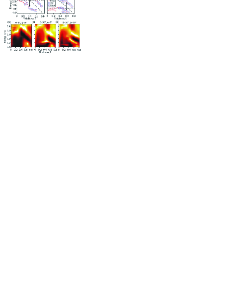
The gap between bonding and anti-bonding mixed plasmons can be seen more clearly in (Fig.3b-d). The three images show the energy dependence of the different modes at increasing void thickness, tracked through the reflectivity, for incident angles of 0∘,30∘. In the latter case we show the thickness dependence for both principal sample orientations. In all cases the drop in energy of the Mie modes can be clearly observed with increasing thickness. At normal incidence, (Fig.3b) the Bragg modes visible around 2.1eV abruptly disappear at while a localized Mie state appears at 1.55eV for . For non-normal incidence, the mode mixing depends on . Examining the two orientations for plasmons travelling either along the necks between voids (, Fig.3c) or along the line of voids (, Fig.3d) reveals the symmetry of the Bragg modes that mix with the plasmons trapped in the voids. In both directions, the lowest Bragg mode (band 1) abruptly vanishes for . For , the next Bragg mode (band 2) around 1.6eV strongly couples to the Mie mode forming a distinctive band gap. Along a high energy mode emerges and drops down into the lowest localized mode at 1.55eV, producing the same band gap. Examining the field distributions suggest that this is the upper Bragg mode (band 6) which has its largest electric field already within the void (Fig.1a).

Thus the scenario of localization on these nanostructured surfaces can be summarized: Bragg plasmons existing in the plasmonic crystal of shallow dishes couple strongly to Mie modes forming new mixed states. Particular Bragg modes whose fields are already stronger in the dishes lose their extended character and drop into Mie plasmons. Bragg modes with fields on the surface vanish at a critical thickness.
These conclusions are confirmed by experiments on a large number of samples of different pitch (and void diameter), and composition. In each case, the Bragg plasmons vanish at a critical thickness just as the lowest localized modes appear (Fig.4). Currently, exact calculation of plasmon energies in arrays of truncated spherical voids is not yet possible, though progress is being made.Teperik05 However, it is interesting to see already the universal features of the experimental plasmon phase diagram (Fig.4b). Plasmon transport is rather different in the regimes of delocalized Bragg modes (coherent plasmon transport with scattering and damping) and localized Mie modes (hopping plasmon transport, enabled by coupling to nearby Bragg modes).
As the Mie modes localize the plasmons, the surface electric fields increase in strength, thus enabling many applications for plasmonic devices. For instance, we have recently shown that these surfaces are ideal for surface enhanced Raman scattering (SERS) which is strongly enhanced in the localised Mie regime.Abdelsalam05 The ability to now predict and engineer appropriate plasmons suited to specific pump and emission wavelengths is a drastic improvement on previous SERS substrates. This approach has proved so promising that it is now in commercial production for a variety of applications in medical and pharmaceutical screening, homeland security and environmental monitoring.Mesophotonics Understanding plasmons on nanostructured surfaces is the gateway to a new generation of nano-plasmonic devices.
We enthusiastically acknowledge discussions with Tatiana Teperick, Sacha Popov, and Javier Garcia de Abajo. This work was supported by EPSRC grants EP/C511786/1, GR/R54194/01. YS was supported by a JSPS Fellowship for Research Abroad, HEISEI 15.
References
- (1) W.L. Barnes, A. Dereux, and T.W. Ebbesen, Nature (London) 424, 824 (2003).
- (2) A.V. Krasavin, A.V. Zayats, and N.I. Zheludev, J. Opt. A: Pure Appl. Opt. 7, 85 (2005).
- (3) A.V. Zayats, and I.I. Smolyaninov, J. Opt. A: Pure Appl. Opt. 5, 16 (2003).
- (4) Z.Q. Tian, B. Ren, and D.Y. Wu, J. Phys. Chem. B, 106, 9463 (2002).
- (5) S.C. Hohng, Y.C. Yoon, D.S. Kim, V. Malyarchuk, R. Müller, Ch. Lienau, J.W. Park, K.H. Yoo, J. Kim, H.Y. Ryu, and Q.H. Park, Appl. Phys. Lett. 81, 3239 (2002).
- (6) T.W. Ebbesen, H.L. Lezec, H.F. Ghaemi, T. Thio, and P.A. Wolff, Nature (London) 391, 667 (1998).
- (7) M.I. Stockman, S.V. Faleev, and D.J. Bergman, Phys. Rev. Lett. 87, 167401 (2001).
- (8) I.R. Hooper, and J.R. Sambles, Phys. Rev. B 65, 165432 (2002).
- (9) D.J. Bergman, and M.I. Stockman, Phys. Rev. Lett. 90, 027402 (2003).
- (10) P.N. Bartlett, P.R. Birkin, and M.A. Ghanem, J. Chem. Soc. Chem. Commun. 2000, 1671 (2000).
- (11) P.N. Bartlett, J.J. Baumberg, S. Coyle, and M. Abdelsalam, Faraday Discussion 125, 19 (2003).
- (12) J.D. Joannopoulos, R.D. Meade, and J.N. Winn, Photonic Crystals (Princeton University Press, Princeton 1995).
- (13) S. Satpathy, Z. Zhang, and M.R. Salehpour, Phys. Rev. Lett. 64, 1239 (1990).
- (14) S. Coyle, M.C. Netti, J.J. Baumberg, M.A. Ghanem, P.R. Birkin, P.N. Bartlett, and D.M. Whittaker, Phys. Rev. Lett. 87, 176801 (2001).
- (15) T.V. Teperik, V.V. Popov, and F.J. García de Abajo Phys. Rev. B 71, 085408 (2005).
- (16) M.C. Netti, M.D.B. Charlton, G.J. Parker, and J.J. Baumberg, Appl. Phys. Lett. 61, 991 (2000).
- (17) S. Coyle, G.V. Prakash, J.J. Baumberg, M. Abdelsalam, and P.N. Bartlett, Appl. Phys. Lett. 83, 767 (2003).
- (18) M. Abdelsalam, P.N. Bartlett, J.J. Baumberg, T.A. Kelf, S. Pelfrey, and A. Russell, Electrochem. Commun. 7, 740 (2005).
- (19) www.mesophotonics.co.uk/products/klariteSERS.html