Integrated optical components on atom chips
Abstract
We report on the integration of small-scale optical components into silicon wafers for use in atom chips. We present an on-chip fibre-optic atom detection scheme that can probe clouds with small atom numbers. The fibres can also be used to generate microscopic dipole traps. We describe our most recent results with optical microcavities and show that single-atom detection can be realised on an atom chip. The key components have been fabricated by etching directly into the atom chip silicon substrate.
pacs:
39.25.+k, 32.80.-t, 42.82.-m, 42.50.PqI Introduction
Atom chips offer a convenient way to miniaturise experiments in atomic physics Hinds and Hughes (1999); Folman et al. (2002). Microstructures on the surface of the chip produce magnetic and/or electric fields, which can be used to confine and manipulate cold alkali atoms near the surface of the chip. Several research groups can now prepare Bose-Einstein condensates (BECs) in microscopic magnetic traps on atom chips. The large field gradients that can be generated near a microstructured surface permit the controlled tunnelling of atoms over micron or sub-micron lengths. This makes the atom chip a natural platform for applications in coherent matter-wave control such as miniaturised atom interferometry Hinds et al. (2001); Hänsel et al. (2001), quantum information processing Calarco et al. (2000), and the study of low-dimensional quantum gases 1Dg (2004). Interaction between the cold atoms and the room temperature surface of the atom chip can be detrimental to applications that require the most sensitive control of the atom. For example, thermal fluctuations of the charges in the conducting chip surface produce magnetic field noise. This can relax atomic spin coherences and populations, thereby destroying the quantum coherence of the atoms Henkel et al. (1999); Jones et al. (2003); Harber et al. (2003); Rekdal et al. (2004); Lin et al. (2004). Furthermore, microscopic imperfections in the materials of the atom chip can cause roughness in the trapping potential, leading in extreme cases to fragmentation of the atom clouds Fortágh et al. (2002); Leanhardt et al. (2003); Jones et al. (2004); Estève et al. (2004). These phenomena are now well understood, and their consequences can be minimised by careful consideration of the chip design. As an example, very recent results from experiments with atom chips based on permanently magnetised patterns on videotape show that the spin-flip-induced loss rate is substantially decreased due to the reduced thickness of conducting material on the chip Curtis, et. al. (2005a, b). Further improvement is expected by using even thinner multilayered films Eriksson et al. (2004). Refinement of fabrication techniques for current carrying wires is also in progress.
With this new understanding and control over atom-surface interactions it is becoming possible to manipulate the quantum states of a few atoms in very tight traps only a few micrometres from the surface of an atom chip. This raises the crucial question of how to detect a few atoms close to the chip. Hitherto, the standard method for probing clouds of trapped atoms has been by absorption imaging or fluorescence detection. The laser light is typically delivered to the chip by external mirrors and lenses. This technique becomes increasingly difficult to utilise as the atom-surface distance becomes small and when the cloud contains very few atoms. Moreover, it is difficult to address individual atoms in this way. Any attempt at constructing a large-scale quantum information processor based on trapped neutral atoms would greatly benefit from a simple detection scheme able to sense a single atom and having high spatial resolution. It is therefore desirable to devise new on-chip detection schemes.
In this paper, we report on our recent efforts towards integrating micro-optical mirrors and fibres into atom chips based on silicon. These components enable us to tailor light fields on the micrometre size-scale, which is commensurate with the relevant trap sizes. Such light fields are well suited for probing a small part of a large atom cloud, or alternatively, for sensing small groups of atoms or single atoms. Some of these components are manufactured as an integral part of the silicon wafer surface and can be used to detect atoms within a few microns from the surface. Control of light fields on this scale also opens up entirely new possibilities for manipulating atoms in microscopic traps.
We have chosen to work with atom chips fabricated on silicon wafers because this material is well understood and many fabrication techniques are already well established. We have been working on a number of devices that use patterns etched into the silicon wafer. Here, we introduce two of them. (i) An atom detector based on a pair of optical fibres mounted in a v-groove etched on the chip wafer. Each fibre can be used to shine light into the other across a small gap where atoms may be placed. A few (5 - 10) atoms in the gap can then be detected, either through the phase shift of the light if it is off-resonant, or through the absorption of near-resonant light Horak et al. (2003). The fibres can also be used to generate a one-dimensional standing wave pattern, making an optical lattice of anti-nodes in which the atoms can be manipulated by the optical dipole force. (ii) We describe a plano-concave optical microcavity where the concave mirror is formed on an etched spherical indentation in the silicon wafer itself. The other mirror is attached to the end of an optical fibre, which acts as the input/output port for light. This permits on-chip single atom detection.
In the next section we describe a typical silicon atom chip into which these structures are being integrated. Section III deals with incorporating optical fibres for on-chip detection of small atom clouds. In section IV we describe optical microcavities that are suitable for single atom detection. We conclude with a summary in section V.
II The magnetic trap atom chip
The silicon chip that we are currently using manipulates the atoms with magnetic fields generated by current carrying wires. The silicon substrate is covered with a 0.6 m thick insulating layer of SiO2. This in turn is covered by a thin Cr adhesion layer and a 5.5 m layer of Au, both deposited by sputtering. This provides a reflective surface for laser light that is used to collect and cool 87Rb atoms in a magneto-optical trap (MOT) in a standard mirror-MOT arrangement. The current-carrying wires are defined lithographically by etching narrow trenches in the Au and Cr layers, a fabrication process that has been described in detail elsewhere Koukharenko et al. (2004).
An image of the chip taken before it was mounted in the vacuum chamber can be seen in Fig. 1. On the chip, four independent wires trace out a Z-shaped patter. When current flows through the wire in the presence of a uniform bias field a Ioffe-Pritchard trap for weak field seeking atoms is formed in the middle of the 7 mm long central section of the Z Reichel et al. (1999). A microscope image of the central section is shown in the inset of Fig. 1. In this part of the chip, there are four parallel wires. The two inner wires are 33 m wide, while the outer pair have a width of 85 m. The centre-to-centre distances are 83 m and 300 m for the thin and thick wire pairs respectively.
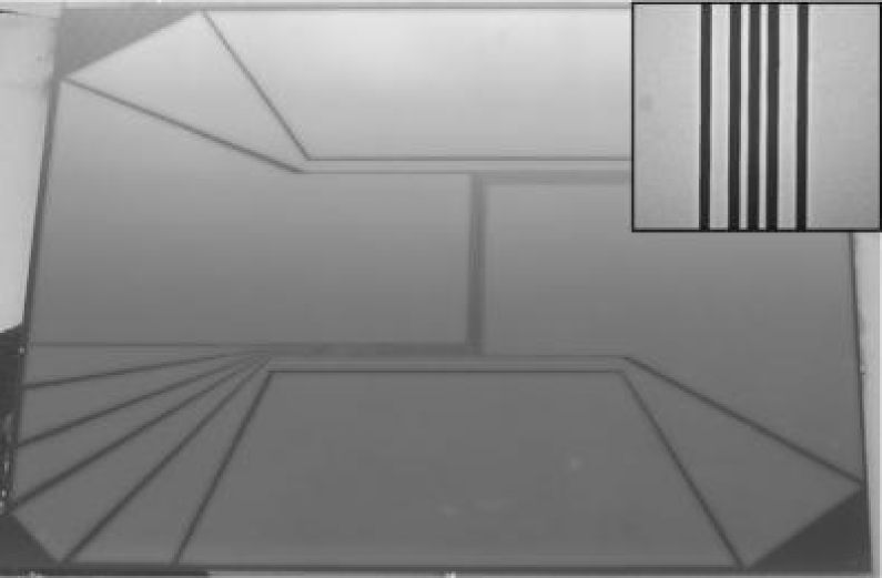
The chip has two additional ‘end-wires’ which run orthogonal to the centre section. These wires can be used to provide additional trap depth, or alternatively to shift the magnetic trap along the Z-wires.
The chip is mounted on a stainless steel base plate, which is in good thermal contact with the vacuum flange. The high thermal conductivity of silicon is a useful feature of this particular chip (for a review of the properties of common materials that are used to manufacture atom chips, the reader should consult Ref. Reichel (2002)). In ultra-high vacuum, the two inner wires can each carry currents up to 1.7 A for one second with only a few degrees increase in temperature. The corresponding current limit for the outer Z-wires is 2.5 A, whilst for the end-wires it is 8.0 A. With all wires at these currents, a magnetic trap 1 mm from the chip surface has a trap depth of approximately 1 mK which is sufficient to hold a laser cooled cloud produced in the MOT.
All six wires on the chip can be independently controlled. With the appropriate choice of wire currents and bias fields, the atom cloud can be moved around on the chip and split in various ways. This kind of control over the cloud is essential for many of the experiments that will be performed with the optical components described in the next sections of this paper.
III Fibre-optic detection of atoms
In principle, fluorescence could be used to detect small numbers of atoms, but it is difficult to achieve a high collection efficiency and each scattering event heats the atom, whether or not the scattered photon is detected. The alternative is to use a directed light beam, which can be efficiently collected and used to measure the absorption or phase shift due to the atoms. Signal-to-noise arguments show that the latter method is typically preferable, provided the cross-sectional area of the light beam is made small enough Horak et al. (2003). A suitably tight waist can be achieved using a tapered optical fibre, as illustrated in Fig. 2 (a), which has a focal spot at a working distance from the tip of the fibre.
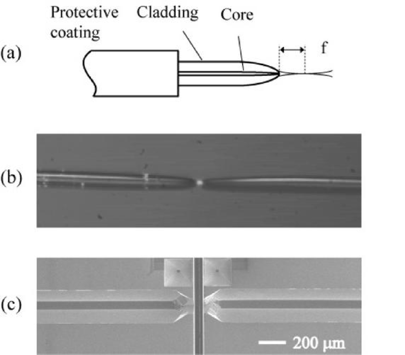
Over most of its length, the fibre we use is a standard 780 nm single-mode fibre with a protective acrylate coating and an outside diameter of 250 m. A few millimeters from the end, the protective coating is removed to reveal the 125 m diameter cladding. A few hundred micrometers from the end, both the core and the cladding begin to taper, and the fibre terminates in a curved surface. This leads to a focal spot with an intensity distribution whose full width at half maximum is at the working distance from the fibre tip. We have been working with fibres where m and m.
A single tapered fibre may be used to sense atoms by fluorescence, provided that they are held sufficiently near the fibre tip. This could be achieved, for example, by sending 795 nm light through the fibre to form an optical dipole force trap, tuned to the red side of the 87Rb D1 (52S1/2 - 52P1/2) transition. 87Rb atoms held by a magnetic trap elsewhere on the chip are moved into the detection zone near the focal spot of a fibre and are captured in this trap. Resonant light tuned to the D2 transition at 780 nm is then passed through the same fibre in order to induce fluorescence, some of which is collected by the fibre and appears as reflected light. Unfortunately, even in the absence of atoms there is a background of reflected light which is difficult to reduce below the level of of the input. With careful filtering of the reflected trapping light this method has the capability to detect several tens of atoms.
A much better scheme is to use two fibres, mounted face-to-face. Fig. 2 (b) shows a microscope image of the arrangement, with light propagating between two tapered fibres. After adjusting the focal spots to coincide we are able to obtain fibre to fibre coupling efficiencies of up to 87 %, more than enough for detection by absorption to become feasible. The situation is now very similar to standard absorption imaging, except that detection takes place in a small, well-localised part of the atom chip. A second important difference is that every photon in the light beam passes through a waist of small area 6 m2. The resonant absorption cross section is roughly 20 times smaller than this, resulting in a absorption for each atom in the waist of the light beam. This method is suitable for detecting 5-10 atoms. An alternative version of this detector is to use non-resonant light and to measure the optical phase shift due to the non-resonant interaction. This has a similar limit of detection sensitivity, as discussed in Ref. Horak et al. (2003).
In order to establish good mechanical stability and alignment of the fibres on the atom chip, we etch v-grooves into the silicon substrate. Fig. 2 (c) shows a scanning electron microscope (SEM) micrograph looking down on them. The length of each groove can be several centimetres and its width is chosen to fit the optical fibre stripped down to its cladding. Fig. 2 (c) shows the central 2 mm, which on this particular chip includes a trench for an atom guide wire (the dark vertical rectangular feature). Near the centre, where the fibres come to within a few tens of micrometers of one another, the groove becomes narrower to support the tapered fibre ends. The grooves are manufactured by depositing masking layers of 40 nm of SiO2 and 160 nm of SiN on a clean silicon wafer. The surface is photolithographically patterned to make openings that have a rectangular shape with constant width for most of the length. Near the fibre tips, the width of the opening in the mask is stepped down to match the narrower tapered ends of the fibers. The masking layer is removed in these areas by dry etching, leaving windows through which the silicon is then wet etched, using 30 % KOH by volume at 70 ∘C. The etching time is optimised to create a groove of the desired depth.
This structure of two fibres in a v-groove can also be used to generate optical lattices in one dimension by guiding light through both fibres. We propose to use this geometry to create a Mott-insulator transition Greiner et al. (2002) on an atom chip. The basic idea is to increase the optical lattice intensity adiabatically from zero in the presence of a BEC between the fibre ends. A key point here is that the small transverse dimension of the light beam allows the volume of each well in the lattice to be small. This ensures an atom-atom repulsion energy in the kHz domain, allowing the transition to be achieved adiabatically on the millisecond timescale. Once the cloud has made the transition into a Mott state, the fibres can be used for detection of the atom ordering by coherent Bragg scattering from the lattice.
IV Optical microcavities
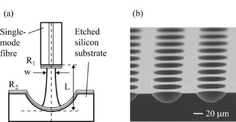
In order to bring the optical detection sensitivity down to one atom, the light beam needs to pass several times back and forth through the region where the atom is located. In other words, we require an optical cavity. For the purpose of detecting one atom it is not necessary to have a cavity with particularly high finesse provided the waist size is small. In that case, the main challenge lies in constructing cavities that can be integrated on the atom chip. To this end, we have been working on plano-concave microcavities with the curved mirror etched into the silicon wafer. The plane mirror is a flat, cleaved fibre tip with a high reflectivity coating applied to it. The general scheme of the cavity is illustrated in Fig. 3 (a). The concave mirror of the cavity is fabricated by means of isotropic etching, a widely used technique in micromachining in which the silicon wafer is etched at approximately the same rate in all directions. The etching solution is continuously stirred during the etching process, resulting in a surface that is approximately spherical. The etchant is a mixture of hydrofluoric acid (H) and nitric acid (N), diluted in acetic (A) acid. The surface morphology and etch rate produced by these chemicals are highly dependent on the concentration of each component, and on the agitation. The relative amounts we prefer to use are H:N:A = 9:75:30 by volume. Further details of the fabrication process can be found elsewhere Moktadir et al. (2004). An SEM micrograph of a typical array of spherical mirror templates is shown in Fig. 3 (b). In order to investigate cavities of various lengths, we have adjusted the etching parameters to produce wafers with a range of mirror radii between 50 and 250 m. The etched surface typically has an RMS roughness of 5 nm, as measured by atomic force microscopy, often with some areas noticeably better than others. For our first measurements, we sputtered an adhesion layer of Cr onto these substrates, followed by 100 nm of Au. After sputtering, the roughness increased to 10 nm.
The plane mirror of the cavity, which acts as the input coupler, is made by gluing a dielectric multilayer transfer coating onto the plane cleaved end of a single-mode 780 nm optical fibre (mode size 2.7 m). We have chosen a coating with a reflectivity of = 98-99% for light in the near infrared range of the spectrum in order to match the reflectivity of gold in this wavelength range. The coating layer is transferred from a glass plate (to which it is loosely attached by adhesion with a dense saline solution) by applying an index-matched optical epoxy to the fibre tip. After the epoxy has set, the tip is pulled away from the glass plate, breaking the coating around the tip edges.
In order to investigate the optical properties of the cavity, 780 nm light from a diode laser is coupled into the fibre, which is aimed at a gold-coated mirror. The silicon wafer is translated longitudinally by a piezoelectric stack to produce a sweep that can cover several cavity fringes and the reflected intensity is monitored. Fig. 4 shows the reflected light signal as a cavity of length = 120 m is scanned over one free spectral range (FSR). In this experiment the curved mirror had a 180 m radius of curvature and the finesse (FSR/) was 102.

Taking the fringe visibility together with the value of the finesse, we calculate that the (intensity) reflectivities of the mirrors are and . The value of corresponds closely to the value specified by the manufacturer of the transfer coating. We attribute the low value of to the surface roughness of the convex mirror. Even so, this cavity is already good enough to detect single atoms. When weakly illuminated with light, we calculate that the amplitude of the reflection dips decreases by a factor of 5 if an atom is introduced into the cavity Kuhn and Rempe (2002).
For future applications in quantum information processing, it would be useful to achieve strong coupling between the atom and the optical microcavity. With this in mind we have started to investigate how high the finesse of these cavities can be made. As a first step in this direction we have put a dielectric coating on one of the silicon wafers and have used a higher-reflectivity transfer coating on the fibre. First results show a finesse in excess of 3,000 on selected mirrors, opening the way to new cavity QED experiments on a chip.
Further work is necessary to incorporate the cavity into an operating atom chip so that it can be loaded with atoms. In order to fine tune the cavity on the chip we have been developing a micro-actuator, which allows the translation of the concave mirror in all three directions of space Gollasch et al. (2005). The translation range of the cavity mirror in the chip plane is large enough to compensate for any mismatch of the optical axes of the cavity mirrors. The cavity length can be tuned to sweep over several cavity fringes.
V Summary
We have presented optical micro-components that can be integrated into atom chips. We have investigated the properties of a fibre-optic detection scheme and shown that clouds with small atom numbers can be probed. We have also developed a high-finesse optical micro-resonator and have shown that it is suitable for single atom detection on a chip, coupled to the external world by a fibre. Silicon is the substrate material that we have used to develop these new optical components because that is the basis of some working atom chips. However, our techniques are probably applicable to any substrate that can be etched or micro-machined. The challenge from the micro-fabrication side of the work lies in the assembly of the various micromachined components of the atom chip, such as the three-axis actuator, the gold wires, the detection cavities and the v-grooves for the optical fibres. This will require bonding of several silicon wafers with good alignment (of the order of a few micrometres). Work is in progress to produce an atom chip that incorporates these various components.
Acknowledgements.
The authors would like to thank Jon Dyne for expert technical assistance. This work is supported by the UK Engineering and Physical Sciences Research Council, the Royal Society, and by the FASTNET and QGATES networks of the European Union.References
- Hinds and Hughes (1999) E. A. Hinds and I. G. Hughes, J. Phys. D: Appl. Phys. 32, R199 (1999).
- Folman et al. (2002) R. Folman, P. Krüger, J. Schmiedmayer, J. Denschlag, and C. Henkel, Adv. At. Mol. Opt. Phys. 48, 263 (2002).
- Hinds et al. (2001) E. A. Hinds, C. J. Vale, and M. G. Boshier, Phys. Rev. Lett. 86, 1462 (2001).
- Hänsel et al. (2001) W. Hänsel, J. Reichel, P. Hommelhoff, and T. W. Hänsch, Phys. Rev. A 64, 063607 (2001).
- Calarco et al. (2000) T. Calarco, E. A. Hinds, D. Jaksch, J. Schmiedmayer, J. I. Cirac, and P. Zoller, Phys. Rev. A 61, 022304 (2000).
- 1Dg (2004) J. Phys. IV France 116, ‘Quantum Gases in Low Dimensions’ (L. Pricoupenko, H. Perrin and M. Olshanii, Eds.) (2004).
- Henkel et al. (1999) C. Henkel, S. Pötting, and M. Wilkens, Appl. Phys. B 69, 379 (1999).
- Jones et al. (2003) M. P. A. Jones, C. J. Vale, D. Sahagun, B. V. Hall, and E. A. Hinds, Phys. Rev. Lett. 91, 080401 (2003).
- Harber et al. (2003) D. M. Harber, J. M. McGuirk, J. M. Obrecht, and E. A. Cornell, J. Low Temp. Phys. 133, 229 (2003).
- Rekdal et al. (2004) P. K. Rekdal, S. Scheel, P. L. Knight, and E. A. Hinds, Phys. Rev. A 70, 013811 (2004).
- Lin et al. (2004) Y. Lin, I. Teper, C. Chin, and V. Vuletić, Phys. Rev. Lett. 92, 050404 (2004).
- Fortágh et al. (2002) J. Fortágh, H. Ott, S. Kraft, A. Günther, and C. Zimmermann, Phys. Rev. A 66, 041604(R) (2002).
- Leanhardt et al. (2003) A. E. Leanhardt, Y. Shin, A. P. Chikkatur, D. Kielpinski, W. Ketterle, and D. E. Pritchard, Phys. Rev. Lett. 90, 100404 (2003).
- Jones et al. (2004) M. P. A. Jones, C. J. Vale, D. Sahagun, B. V. Hall, C. C. Eberlein, B. E. Sauer, K. Furusawa, and D. Richardson, J. Phys. B: At. Mol. Opt. Phys. 37, L15 (2004).
- Estève et al. (2004) J. Estève, C. Aussibal, T. Schumm, C. Figl, D. Mailly, I. Bouchoule, C. I. Westbrook, and A. Aspect, Phys. Rev. A 70, 043629 (2004).
- Curtis, et. al. (2005a) E. A. Curtis, et. al., Manuscript in preparation (2005a).
- Curtis, et. al. (2005b) E. A. Curtis, et. al., Submitted to the topical issue on atom chips of the European Phys. J. D (2005b).
- Eriksson et al. (2004) S. Eriksson, F. Ramirez-Martinez, E. A. Curtis, B. E. Sauer, P. W. Nutter, E. W. Hill, and E. A. Hinds, Appl. Phys. B 79, 811 (2004).
- Horak et al. (2003) P. Horak, B. G. Klappauf, A. Haase, R. Folman, J. Schmiedmayer, P. Domokos, and E. A. Hinds, Phys. Rev. A 67, 043806 (2003).
- Koukharenko et al. (2004) E. Koukharenko, Z. Moktadir, M. Kraft, M. E. Abdelsalam, D. M. Bagnall, C. Vale, M. P. A. Jones, and E. A. Hinds, Sensor. Actuat. A-Phys. 115, 600 (2004).
- Reichel et al. (1999) J. Reichel, W. Hänsel, and T. W. Hänsch, Phys. Rev. Lett. 83, 3398 (1999).
- Reichel (2002) J. Reichel, Appl. Phys. B 75, 469 (2002).
- Greiner et al. (2002) M. Greiner, O. Mandel, T. Esslinger, T. W. Hänsch, and I. Bloch, Nature 415, 39 (2002).
- Moktadir et al. (2004) Z. Moktadir, E. Koukharenka, M. Kraft, D. M. Bagnall, M. Jones, H. Powell, and E. Hinds, J. Micromech. Microeng. 14, 1 (2004).
- Kuhn and Rempe (2002) A. Kuhn and G. Rempe, in Experimental Quantum Computation and Information, edited by F. de Martini and C. Monroe (IOS Press, Amsterdam, 2002), Proc. Int. School of Physics Enrico Fermi, course CXLVIII, pp. 37–66.
- Gollasch et al. (2005) C. O. Gollasch, Z. Moktadir, M. Kraft, D. M. Bagnall, M. Trupke, S. Eriksson, and E. A. Hinds, To appear in J. Micromech. Microeng. (2005).