Measurement of the Charge Collection Efficiency after Heavy Non-Uniform Irradiation in BABAR Silicon Detectors
Abstract
We have investigated the depletion voltage changes, leakage current increase and charge collection efficiency of a silicon microstrip detector identical to those used in the inner layers of the B A B AR Silicon Vertex Tracker (SVT) after heavy non-uniform irradiation. A full SVT module with the front-end electronics connected has been irradiated with a 0.9 GeV electron beam up to a peak fluence of 3.51014 /cm2, well beyond the level causing substrate type inversion. We have irradiated the silicon with a non-uniform profile having =1.4 mm that simulates the conditions encountered in the B A B AR experiment by the modules intersecting the horizontal machine plane. The position dependence of the charge collection properties and the depletion voltage have been investigated in detail using a 1060 nm LED and an innovative measuring technique based only on the digital output of the chip.
Index Terms:
radiation damage, silicon detectorI Introduction
Several tests have been performed in the past to study the effects of radiation damage to the B A B AR Silicon Vertex Tracker (SVT) sensors and to their front-end electronics [1], but the reduction of charge collection efficiency (CCE) after irradiation has never been measured quantitatively. In addition, it has never been directly demonstrated that a SVT module can be operated normally after substrate type-inversion. This is expected to happen at a dose of Mrad, based on measurements performed on test structures from the same wafers. To address these issues a module identical to those used in the inner layer of the SVT, with the front-end electronics connected, has been irradiated with a 0.9 GeV electron beam. A total peak fluence of , corresponding to a peak dose of 9.3 Mrad, has been delivered to the silicon. A second module, which has not been irradiated, has been used as a control sample to track variations in the environmental conditions.
II Radiation damage of the SVT
The B A B AR experiment [2], at the SLAC PEP-II storage ring [3], has the primary physics goal of precisely measuring -violating asymmetries and rare branching fractions in meson decays. pairs are produced in head-on collisions between 9.0 GeV electrons and 3.1 GeV positrons. Since a very large sample of decays is needed, PEP-II was designed to deliver the high peak luminosity of (the production cross section is = 1.1 nb)
The Silicon Vertex Tracker [4] was installed in B A B AR in early 1999 and has been reliably operated for five years, providing excellent and efficient vertexing and tracking information. It is composed of five layers of 300 m thick, double-sided microstrip detectors. p+ strips on one side and orthogonally-oriented n+ strips on the other side are implanted on a high-resistivity n- bulk. They are AC-coupled to the electronics via integrated decoupling capacitors. The detectors are operated in reverse mode at full depletion, with bias voltage typically 10 V higher than the depletion voltage (which lies in the range 25 V – 35 V). The leakage current per unit area under these conditions, prior to installation in B A B AR, is lower than 100 nA/cm2 at room temperature.
The main source of background in the SVT comes from electromagnetic showers originating in the material of the beam-line by off-momentum beam particles (), which are over-bent by the permanent dipole magnets located in the proximity of the interaction point to separate the two beams. A significant fraction of this background is expected to be composed of electrons and positrons with energies of a few hundreds of MeV. Their non-ionizing energy loss (NIEL), using the asymptotic value of the displacement cross section for 200 MeV calculated in [5], is about twelve times lower than that of 1 MeV neutrons at equal fluence, and the NIEL-normalized damage constant /NIEL has been estimated in previous measurements to be about one third than that of neutrons [1]:
| (1) | |||
| (2) |
The dose absorbed by the silicon, which is measured by means of 12 silicon p-i-n diodes close to the inner layer of the SVT, varies strongly as a function of the azimuthal angle around the beamline, and is highly peaked in a narrow region of the (horizontal) bend plane of the machine, following a roughly gaussian distribution with mm. The inner layer of the SVT, located at a radius of 3.3 cm from the beam line, receives the highest dose. At design luminosity the average dose for the silicon of the inner layer was expected to be 33 krad/yr, peaking to 240 krad/yr in the horizontal region. The detectors were therefore originally designed to withstand up to 2 Mrad of total radiation dose, which would have been reached in ten years of running only in the inner horizontal region of the SVT, and which is expected to be less than the dose at which bulk type-inversion occurs. However, excellent PEP-II performance has been significantly higher than expected. The peak instantaneous luminosity has reached , three times the design value, and is expected to increase up to . A thin horizontal region of the inner part of the detector has thus already received the dose budget of 2 Mrad and will receive 9 Mrad by 2009, whereas a larger fraction of silicon in the inner layers away from the horizontal plane should accumulate a dose between 2 and 5 Mrad by the same date.
III Principle of the CCE measurement
The basic idea of the measurement is to use a 1060 nm LED, whose attenuation length mm is deeper than the 300 m of the silicon thickness, to generate charges in the sensors. The charges then drift in the fully depleted silicon and the signals induced on the microstrip electrodes on the two sides of the detectors are amplified by the front-end electronics.
Each readout strip of the sensors, whose pitch is 50 m on the n-side and 100 m on the p-side, is connected to one of the 128 channels of the AToM IC [6]. The AToM IC is a custom readout chip produced with a Honeywell rad-hard 0.8 m CMOS process. It is capable of simultaneous acquisition, digitization and readout. Each channel of the AToM IC, as shown in Figure 1, has an analog section consisting of a low-noise charge-sensitive pre-amplifier followed by a CR-(RC)2 shaper, whose output is coupled differentially into a comparator. The nominal gain of the pre-amplifier is 250 mV/fC. The shaping time is programmable, with a minimum of 100 ns, up to 400 ns. In our measurements we used the 100 ns setting, which is also used in the modules in the inner layers of the SVT. The comparator threshold is controlled by an on-chip 6-bit DAC (Thresh DAC) whose least significant bit (LSB) has a nominal value of 12.5 mV, corresponding to a charge of 0.05 fC at the pre-amplifier’s input. The comparator output goes to an SRAM pipeline, which provides a trigger latency of 12.93 s. When the input to the comparator exceeds the pre-set threshold, the output goes high and a series of ones is clocked into the pipeline. A calibration charge can be injected into the preamplifier by means of a 50 fF capacitor (Cinj) connected with a switch to the pre-amplifier input and controlled by a 6-bit DAC (CAL DAC). The CAL DAC LSB has a nominal value of 10 mV, corresponding to a charge on Cinj of 0.5 fC.
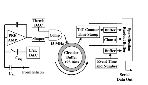
Upon receipt of an external trigger, a selectable region in the pipeline is searched for a zero-to-one transition. The transition indicates a “hit” and the number of following ones at the comparator output, divided by the clock period, represents the time-over-threshold (TOT) of the hit, which is stored as a 4-bit number and has an approximately logarithmic dependence on the input charge. This allows charge measurement over a broad dynamic range ( 40 fC) with a limited number of bits, but the limited accuracy makes the TOT unsuitable for the purpose of our measurement, where a good analog resolution is needed in order to establish small drops in the CCE. Therefore we have turned to an alternative method of measuring the charge, based on “threshold scans” [7].
A threshold scan consists in measuring, for each read-out channel at fixed injected charge at the input of the pre-amplifier, the hit efficiency as a function of the pre-set threshold of the comparator, which is varied inside the full dynamic range. The 50% turning point of the hit efficiency versus threshold distribution is the threshold offset for the channel at charge , as shown in Figure 2.
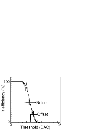
The threshold offset has a linear dependence on the charge which is given by the following expression:
| (3) |
The pedestal and the gain of the -th electronic channel can be accurately determined by means of calibration threshold scans, in which the silicon is not illuminated by the LED, and a known amount of charge is injected at the input of the pre-amplifier by closing the switch which connects it to the 50 fF capacitor Cinj. and are found by performing calibration threshold scans with different known charges and fitting the vs distribution with a linear function.
When the LED is used to generate charge in the silicon, the charge at the input of the pre-amplifier of the -th channel is , where is the total charge release by the LED in the silicon, which is proportional to the LED intensity, is the local charge collection efficiency of the detector and accounts for division of the charge between the channels and the angular distribution of the LED power. When the detector is fully depleted and the electric field intensity is sufficient to collect almost all the charge, (for both sides) and the CCE, as a function of the reverse bias voltage applied to the silicon, saturates. In our case the LED is current-driven and the light flux is proportional to the LED current, therefore . In a threshold scan performed with the silicon illuminated by the LED with current therefore the offset of the -th channel is given by
| (4) |
From threshold scans at different values of the LED current one can extract for each channel the slope by performing a linear fit to the vs distribution. By dividing the slope for the electronics gain and summing over all channels we obtain therefore a quantity which is proportional to the average CCE in the silicon region illuminated by the LED:
| (5) |
By comparing the sum before and after the irradiation of the detectors we can therefore monitor the relative CCE drop.
IV Experimental setup
IV-A Setup for the CCE measurement
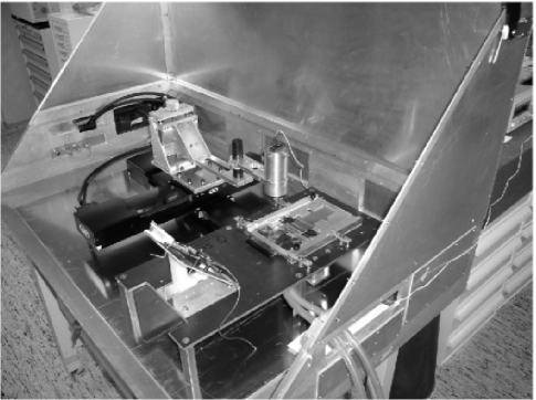
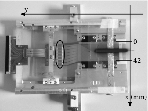
The LED is a current-driven EG&G C30116 model, with peak wavelength = 1060 nm, risetime 10 ns, typical peak flux vs LED current mW/A. It is connected through a 1 k resistor to a GPIB-controlled pulser. A thin brass foil with a 500 m diameter pinhole is placed at a distance of 3 mm from the LED lens surface. A converging lens with focal length = 45 mm is placed at a distance of 90 mm from the pinhole and at the same distance from the module plane, thus ensuring that the pinhole image is focused in the module plane. In our measurements the light emitted from the LED enters the silicon from the n+-doped (ohmic) side. The dimension of the luminous spot has been chosen to be narrower than the region in which the CCE, after irradiation with a beam with 2 mm, is supposed to change, but at the same time it is large enough that the uncertainty in the relative alignment of the LED and the silicon detectors (100 m) has a negligible impact on the uncertainty on the measured CCE. The LED, the pinhole and the lens are mounted inside a brass cylinder attached to a mechanical arm of a GPIB-controlled X-Y stage. A picture of the mechanical setup is shown in Figure 3.
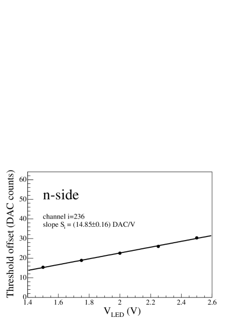
The charge generated in the silicon is controlled by changing the amplitude of the pulse driving the LED. We have selected a range of amplitudes in which the LED response is linear and the signal at the shaper output remains within the limited dynamic range of the THR-DAC, as shown in Figure 4.
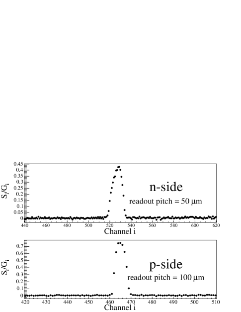
The measurement process is fully automated: a workstation controls the motion of the X-Y stage and the voltage setting of the pulser via GPIB connections, while at the same time controls through an ethernet interface a VME-based computer which is responsible for sending trigger signals to the pulser and to the readout section of the front end electronics. An example of the distribution of vs channel measured with this setup is shown in Figure 5: the peak width is consistent with the pinhole size and the readout pitch of the strips.
Once the distribution has been measured, an offline algorithm identifies the position of the peak, evaluates the baseline in channels away from the peak, and computes the baseline-subtracted sum over the whole peak, which is proportional to the average CCE in the point illuminated by the LED. Repeated tests on the control module have shown that the single measurement resolution is about 2%. Alignment in the relative position between the module and the X-Y stage and aplanarity effects have been found to introduce negligible degradation in the CCE resolution. Moreover, no significant variation (compared to the 2% intrinsic resolution) of the measured CCE has been observed over a period of several hours of continuous operations. However, differences up to 10% have been found in CCE measurements performed in different runs. For this reason the CCE measured for the irradiated module has always been normalized to the average CCE measured, with a high number of samplings, in a fixed set of points of the control module in the same environmental conditions.
IV-B Setup for the silicon irradiation
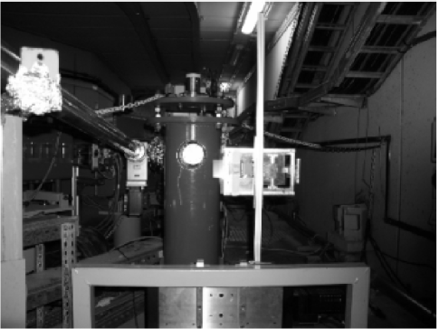
The module irradiation has been performed at the Elettra Synchrotron facility in Trieste with a 0.9 GeV electron beam. The irradiation has been performed in six steps reaching a total peak dose of about 9 Mrad. Two pictures of the module setup are shown in Figures 6 and 7.
During each irradiation step the module is mounted on a X-Y stage, which is located at the end of the Linac and is remotely controlled from the Linac Control Room through a serial connection. The alignment of the module and of the X-Y stage is such that the detector surface lies in a plane orthogonal to the beamline ( axis), and the module can be moved, by means of the X-Y stage, along the and directions. The silicon surface is a rectangle measuring mm in the direction, which is parallel to the orientation of the p+ strips, and 82.6 mm in the direction, which is parallel to the orientation of the n+ strips. The module thickness along the direction is 300 m.
Prior to the irradiation a radiochromic dosimetry film is placed close to the surface of the silicon, to keep track of the beam position during the irradiation. Another radiochromic film is placed above the chip region to check that the electronics does not receive a significant dose, thus avoiding the need in the CCE measurement to disentangle effects caused by radiation damage to the silicon from effects caused by damage to the electronics. A third radiochromic film is attached to the edge of the metal frame which hosts the module and is irradiated for a few seconds (to avoid saturation) to obtain an image of the beam profile, which is necessary to perform the alignment between the detector and the beam and is used to estimate the beam profile. The beam spot obtained with this method is shown in Figure 8. Two sets of test structures from the same wafer as the silicon detectors are mounted on the module frame in a position which corresponds to the center of the zone to be irradiated.
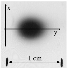
After alignment of the module with respect to the beamline, the linac is turned on and the module is moved back and forth several times in the plane , along a line parallel to the axis. The beam has a gaussian profile whose width along the axis, accurately measured by digitizing and analyzing the spot obtained on the radiochromic dosimetry film irradiated for a few seconds, is 1.4 mm. By moving the module with constant velocity 1 mm/s along , a 50 mm long region of the silicon is irradiated, with a dose profile which is uniform in and gaussian in , centered on the axis of the module and with width equal to the beam width . The beam remains several centimeters from the chips during all the irradiation.
The peak fluence and hence the peak dose are determined from the beam spread, the speed at which the module is moved during the irradiation, the number of times this operation is performed and the linac current through the relation where C is the electron charge. For typical values ( = 1.4 mm, = 1 mm/s, = 30 nA and = 10), a total peak fluence of about /cm2 (corresponding to a peak dose of about 1.4 Mrad) is delivered to the module in about ten minutes. The linac current is measured with 4% accuracy from the current flowing in a toroidal coil coaxial with the beam and is the dominating source of uncertainty in the peak fluence estimate. A less precise dose estimate, obtained from the increase in leakage current in the test structures irradiated with the detector, is used as a cross check and is consistent with the estimate from the linac current.
V Results
V-A Leakage current increase
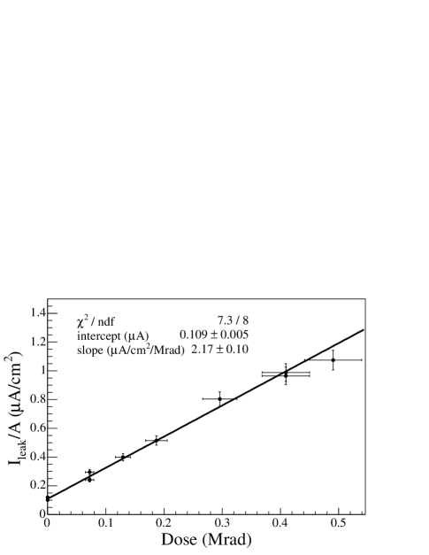
After each irradiation step we have measured the leakage current of the module from standard I-V curves at reverse bias. The leakage current per unit area increases linearly with the accumulated dose of the whole module, as shown in Figure 9. The current increase per unit area vs dose is , normalized at a temperature of C, consistent with the increase observed in the SVT during B A B AR operation. The damage constant , where is the leakage current density and is the average electron fluence delivered to the silicon, is A/cm, normalized at C.
V-B Depletion voltage shift
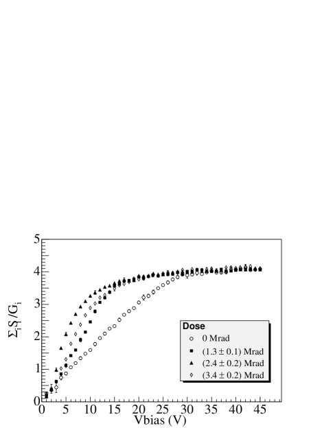
After each irradiation we have measured, at a point in the center of the most irradiated zone of the detector, the sum (which is proportional to the local CCE) as a function of the reverse bias voltage applied to the silicon. This is shown, up to the fifth irradiation step, in Figure 10.
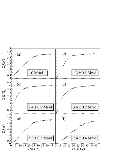
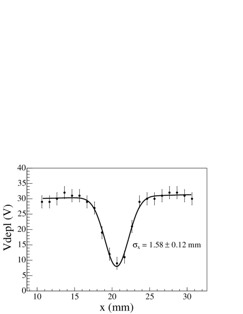
For high values of the bias voltage the vs curve is characterized by a plateau over which the CCE increases very little when the bias voltage is increased, corresponding to the fact that the trapping probability of charge carriers slowly decreases as long as the electric field inside the detector becomes stronger. We use the voltage value below which the sum and therefore the CCE fall below 90% of the plateau value as a rough estimator for the depletion voltage of the silicon in the point illuminated by the LED. As an example, consider the curve shown in Figure 10 (a), measured before the first irradiation step: in that case we estimate V, which is roughly consistent with the depletion voltage V measured in structure tests from the same wafer. is not a good estimator for the depletion voltage when is close to 0 V, because in that case there is a bias voltage range in which the detector is fully depleted but the electric field inside it is not intense enough to approach signal saturation. In that case gives only an upper limit for : indeed, in all our measurements never takes values below 10 V. However, when the depletion voltage is higher than 10 V then is a reasonable estimator for . To confirm that is a reasonable estimator of the depletion voltage, which is shifted by bulk damage of the silicon, we estimate – after the second irradiation step, corresponding to a total peak dose of 2.5 Mrad – in a set of 21 points, equally spaced (at 1mm steps), on a line which is orthogonal to the irradiation direction and crosses the irradiated region. The distribution of , shown in Figure 11, exhibits a clear peak whose width is consistent with the measured beam spread.
From the measured values of at different doses obtained from the CCE vs curves of Figure 10, we see that the depletion voltage in the damaged silicon first decreases with dose, then starts to increase again. This is evident when overlaying the curves in the same plot, as shown in Figure 12. The inversion occurs between Mrad and Mrad: we therefore estimate the inversion point, which corresponds to the bulk type inversion of the silicon, to be at Mrad. After type inversion the detector continues to operate without any problem.
V-C Charge collection efficiency drop
The CCE has been measured, before and after irradiation, in a grid of 30x30 points spanning almost the entire surface of the module. These measurements have been performed with the detector reversed biased with a potential chosen to be at least 10 V higher than the estimated depletion voltage in the most irradiated area of the silicon, to make sure that the silicon is fully depleted everywhere across the detector. The distribution of these points across the detector surface and the ratio between the CCE measured after the last irradiation step and the CCE before irradiation, for the p-side, is shown in Figure 13.
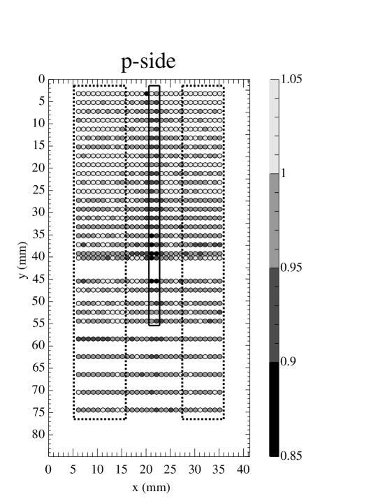
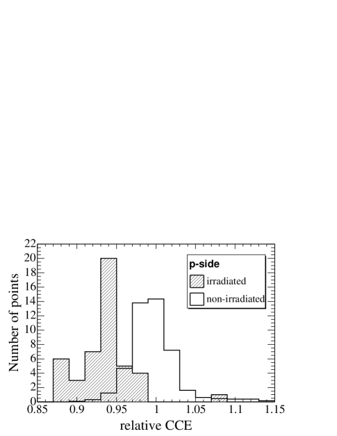
In Figure 14 we compare the CCE drop in points at the center of the irradiated zone, (the solid central rectangle in Figure 13) which have received a total dose of Mrad, with points which are at least 4 away from the irradiation axis and have received a dose of only a few krad. (the two lateral dashed rectangles in Figure 13). For points in the irradiated zone we measure a CCE decrease equal to on the p-side and on the n-side, while no CCE decrease is observed for points which have received a negligible dose.

VI Conclusion
We have irradiated, with a 0.9 GeV beam, a silicon detector identical to those in the B A B AR Silicon Vertex Tracker. We have implemented a fully automated setup by means of which we can generate charge in the silicon through illumination with a 1060 nm LED and measure the charge collection efficiency through an innovative method based on the digital output of the front-end electronics connected to the detector. We have measured an increase in leakage current per unit area at 23∘C of A/cm2/Mrad. The detector, whose initial depletion voltage was 25 V, has undergone type inversion at a dose of Mrad, after which it has continued to operate without any problem. We have measured, in points irradiated with a dose of Mrad, a moderate charge collection efficiency decrease equal to on the p-side and on the n-side. We have thus demonstrated that the SVT sensors can be operated for the whole lifetime of the B A B AR experiment and that bulk damage in the silicon will cause only a modest impact on their performances.
References
- [1] I. Rachevskaia et al., “Radiation damage of silicon structures with electrons of 900 MeV”, Nucl. Instrum. Meth. vol. A485, pp. 126-132, 2002; V. Re et al., “The B A B AR silicon-vertex tracker: performance, running experience, and radiation-damage studies”, IEEE Trans. Nucl. Sci. vol. 49, pp. 3284-3289, 2002.
- [2] B A B AR Collaboration, B. Aubert et al., “The B A B AR detector”, Nucl. Instrum. Meth. vol. A479, pp. 1-116, 2002.
- [3] “PEP-II – An asymmetric Factory, Conceptual Design Report”, SLAC-418, LBL-5379, 1993.
- [4] D. Barbieri et al., “Silicon sensors for the B A B AR Vertex Tracker: Design, Electrical Tests and Production Quality Control”, Nuovo Cimento, vol. A112, pp.113-130, 1999; C. Bozzi et al., “The design and construction of the B A B AR silicon vertex tracker”, Nucl. Instrum. Meth. vol. A447, pp. 15-25, 2000.
- [5] G. P. Summers et al., “Damage correlations in semiconductors exposed to gamma, electron and proton radiations”, IEEE Trans. Nucl. Sci. vol. 40, pp. 1372-1379, 1993.
- [6] V. Re et al, “The Rad-Hard Readout System of the B A B AR Silicon Vertex Tracker”, Nucl. Instrum. Meth. vol. A409, pp. 354-359, 1998.
- [7] C. Campagnari et al (1998, August). Study of SVT gains. [Online]. Available: http://charm.physics.ucsb.edu/BaBar/LedGainStudy.html