Rayleigh scattering, mode coupling, and optical loss in silicon microdisks
Abstract
High refractive index contrast optical microdisk resonators fabricated from silicon-on-insulator wafers are studied using an external silica fiber taper waveguide as a wafer-scale optical probe. Measurements performed in the 1500 nm wavelength band show that these silicon microdisks can support whispering-gallery modes with quality factors as high as , limited by Rayleigh scattering from fabrication induced surface roughness. Microdisks with radii as small as m are studied, with measured quality factors as high as for an optical mode volume of 5.3.
pacs:
42.60.Da, 42.81.QbRecent studies of optical resonators in glass based microspheresVernooy et al. (1998); Weiss et al. (1995); Cai et al. (2000), microringsLittle et al. (1999), and microtoroidsArmani et al. (2003) have highlighted the applications afforded by the extremely long photon lifetime of whispering-gallery-modes (WGMs) supported by these structures. Furthermore, recent work by Ilchenko et al. illustrated the advantages of creating WGMs in crystalline materialsIlchenko et al. (2004). Applications for such devices include quantum networkingKimble (1998), low threshold non-linear optical sourcesSpillane et al. (2002), and compact micro-optical circuitsLittle et al. (1999). The ability to create similar high quality factor () WGM resonators in III-V or silicon (Si) semiconductors has thus far been hampered by the large refractive index of most semiconductors and the resulting sensitivity to surface roughnessGayral et al. (1999); Choi et al. (2004). In this Letter we describe measurements of micron-sized Si microdisk resonators supporting transverse-magnetic (TM) WGMs with significantly reduced sensitivity to disk-edge roughness. These modes have measured values as high as and effective modal volumes () as small as cubic wavelengths in the material. The largest ratio is measured to be , greater than the values measured in ultra-small volume photonic crystalsSrinivasan et al. (2003) and comparable to the values measured in ultra-high- microspheres and microtoroidsVernooy et al. (1998); Armani et al. (2003); Ilchenko et al. (2004).
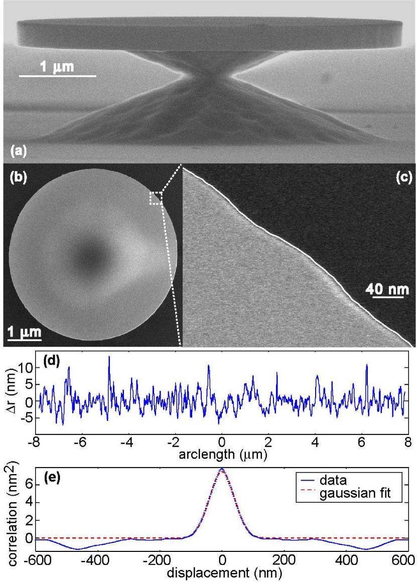
The silicon microdisks in this work are fabricated from a silicon-on-insulator (SOI) wafer consisting of a nm thick p-doped Si layer of resistivity 1-3 -cm atop a two micron SiO2 layer. Processing of the microdisks begins with the deposition of a 20 nm SiO2 protective cap layer using plasma-enhanced chemical-vapor-deposition. Electron beam lithography is used to create a polymer resist etch mask, and a low-bias voltage inductively-coupled-plasma reactive-ion-etch with SF6:C4F8 gas chemistrySrinivasan et al. (2003) then transfers the circular microdisk pattern into the top Si layer. After dry-etching, the sample is immersed in buffered hydrofluoric acid to undercut the bottom SiO2 cladding, as shown in Figure 1. The thin nm SiO2 top cap layer is also removed in this process, providing a clean, smooth top Si surface. A final rinse in deionized water is performed, followed by a high-purity nitrogen spray drying step.
In order to characterize the microdisk resonators, an evanescent fiber taper coupling technique is employedSrinivasan et al. (2003). In this process, an optical fiber is adiabatically drawn to a 1-2 m diameter so that its evanescent field is made accessible to the environment. In this work, the fiber taper is positioned to the side of the microdisks, with a center height equal to that of the middle of the microdisk. Measurements of the taper transmission as a function of the lateral taper-microdisk gap () are then performed using a swept wavelength tunable laser source ( 1509-1625 nm) with fine frequency resolution of MHz. A set of paddle wheels are used to adjust the polarization state of the fiber taper mode in the microdisk coupling region, providing selective coupling to the TE-like (TM-like) WGMs with dominant electric field parallel (normal) to the plane of the microdisk. For the 344 nm Si layer thickness of the microdisks studied here, only the fundamental vertical slab mode for TE and TM polarization are strongly guided. As such, we only consider the fundamental vertical modes of the microdisks in what follows, labeling them simply by , where is either TE or TM, and and are the characteristic radial and azimuthal number, respectivelyLittle and Chu (1996).
Microdisks of two different sizes, radius and m, are fabricated and tested. A broad wavelength scan covering the 1509-1625 nm wavelength range is initially employed to map out the different microdisk modes. As will be detailed elsewhereBorselli and Painter (2004), the adjustable polarization state in the taper along with the WGMs’ strength of coupling and linewidth is used to determine sets of modes with a common free spectral range. These measurements provided a reliable determination of radial mode number. An effective index two-dimensional model is then used to estimate the azimuthal number. Using this mode identification technique we found that the highest modes in both sizes of microdisks are consistently of TM polarization, and corresponded to the lowest radial number, .
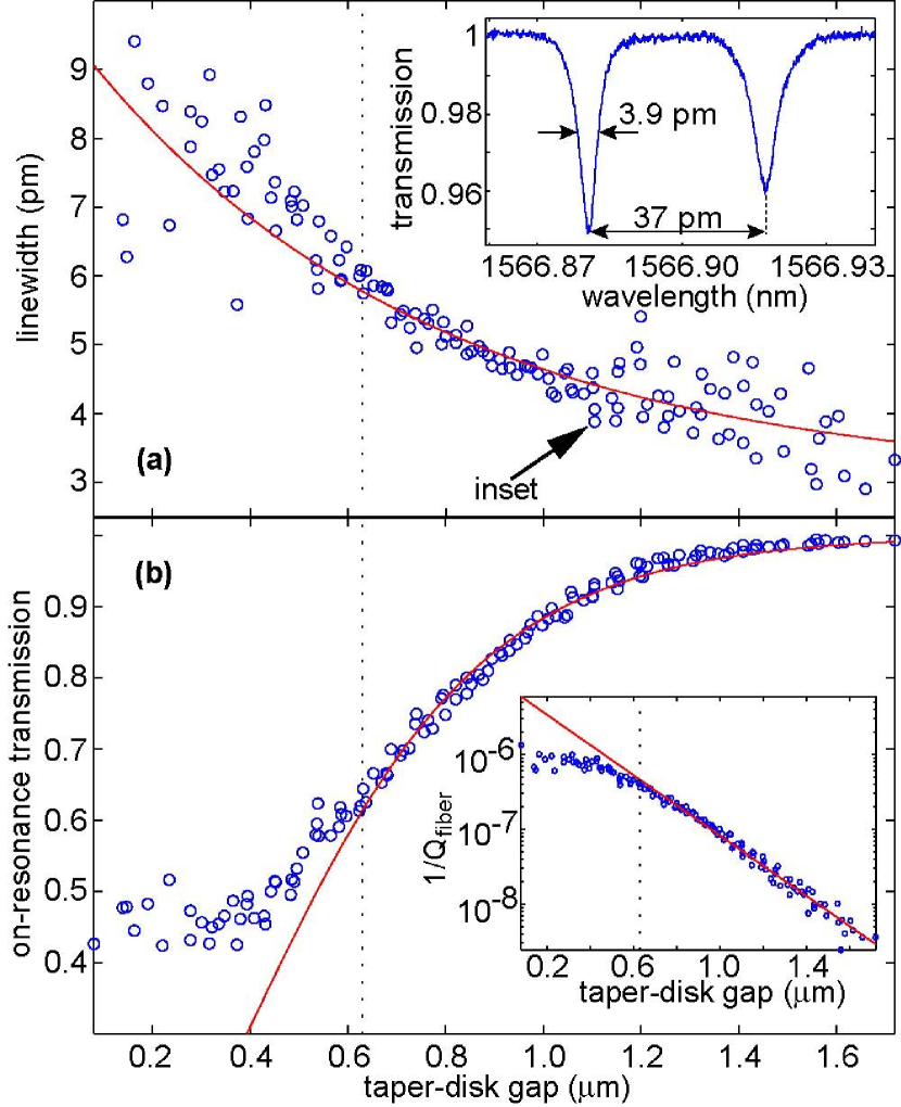
The inset of Fig. 2(a) shows the evanescent coupling to a WGM of a m microdisk, with tapered fiber positioned 1.1 m laterally from the disk edge. The observed double resonance dip (doublet) is a result of Rayleigh scattering from disk surface roughness as discussed below, which lifts the degeneracy of clockwise () and counter-clockwise () propagating WGMs in the microdiskWeiss et al. (1995). Fitting the shorter wavelength mode of the doublet to a Lorentzian yields a loaded linewidth of pm with a coupling depth. These measurements are repeated for varying taper-microdisk gaps and are recorded in Figure 2(a,b). For m, the data follows a two-port coupled mode theory with simple exponential loading dependence on taper-microdisk gapCai et al. (2000). Fits based upon this model are shown as a solid line in each of the plots of Fig. 2. The fiber loading of the microdisk is characterized here by a dimensionless effective quality factor, (inset to Fig. 2(b)). The asymptotic unloaded linewidth is found to be pm for this WGM, corresponding to a bare-cavity of . The observed non-exponential loading dependence for small is due to the large phase mismatch between the glass fiber and Si microdisk modes, further studies of which will be presented elsewhereBorselli and Painter (2004).
| (pm) | |||
|---|---|---|---|
| exp. (th.) | exp. (th.) | ||
Similar measurements are performed for all modes (of both polarizations) in each of the two different microdisk sizes, and a summary of the measured bare-cavity and doublet mode-splitting values are given in Table 1. In order to understand the limiting loss mechanisms and the observed trend of with polarization and radial mode number, a complementary theoretical analysis is also performed. Both the radiation limited (Spillane (2004)) and the free carrier absorption of the p-doped Si disk layer (estimated to be from Ref. Soref and Lorenzo (1986)), are far greater than the measured values. Surface state absorption is another possible loss mechanism; however, several trials are performed with differing final chemical cleaning steps with no perceivable change in . The rather large measured splitting of the and traveling wave modes indicates strong surface scatteringGorodetsky et al. (2000), and therefore we believe the dominant source of optical loss to be scattering from index perturbations at the microdisk surface.
Surface roughness on the top and bottom surfaces of the microdisks analyzed in this work is negligible in comparison to the azimuthal variation of the disk radius [Fig. 1(c)], a result of mask erosion and deformation during the dry etching step. For this type of roughness, the index perturbation can be approximated by , where is the free space permittivity, , is the Si refractive index, is the index of the surrounding air, is the disk height, and is the radial surface roughness relative to the unperturbed disk radiusLittle and Laine (1997). The parameters , , and correspond to the radius from the disk center, arc length along the disk perimeter, and height along the disk edge, respectively. These perturbations of the disk radius set up polarization currents, , which couple the WGMs of the perfect microdisk to radiation modes or other nearly resonant WGMs. The Volume Current MethodKuznetsov and Haus (1983) can be used to calculate the radiated power into free space from , providing an estimate for the surface-scattering quality factor, . In the limit that the correlation length of the roughness () is much smaller than the wavelength in the material,
| (1) |
where , is the average -polarized electric field energy density at the disk edge normalized to unit modal energy, is the standard deviation of the roughness, and is a geometrical radiation factor for the different electric field polarizations. The mode coupling between counterpropagating and traveling wave modes can also be found via a time-dependent perturbation theoryGorodetsky et al. (2000). This coupling breaks the degeneracy of the and modes (), creating two standing wave modes with wavelength splitting
| (2) |
where . SEM micrographs such as those shown in Figs. 1(b,c) provide high contrast images from which edge contours with near nanometer resolution can be obtained [Fig. 1(d)]. From a Gaussian fit to the autocorrelation function of the surface roughness [Fig. 1(e)], estimates for and are found to be nm and nm, respectively, typical of the fabricated microdisks in this work. Using the results from this roughness analysis in Eqs. (1) and (2), theoretical estimates for and are calculated and tabulated in Table 1, with good agreement found between theory and the measured microdisk properties. In these calculations, an effective index model based on Ref. Little and Chu (1996) is used to estimate and the effective mode volume not , with the approximate TM modes given by a single field component and the TE modes consisting of and electric field components. The salient result of this analysis is that a TE mode has roughly three times the radiated power versus a comparable TM mode. This is explained by the fact that both the and components couple to radiation modes more strongly than the component of the field. The modes of higher number are also measured and found to be lower as predicted by the disk-edge surface-scattering theory, although for the effects of the underlying SiO2 pedestal may be significant.
In summary, Si microdisks of a few microns in radius have been fabricated with measured . In contrast to theoretical predictions for an ideal microdisk, we find that the TM modes have significantly higher measured values than TE modes due to their inherent reduced sensitivity to disk-edge surface roughness. In comparison to previously measured high- semiconductor microdisks Gayral et al. (1999), the of the smallest WGMs measured in this work are times larger while maintaining a similar effective mode volume.
The authors thank S. Spillane, T. Johnson, and H. Huang for helpful contributions to this work. M.B. thanks the Moore Foundation, NPSC, and HRL Laboratories, and K.S. thanks the Hertz Foundation for their graduate fellowship support.
References
- Vernooy et al. (1998) D. W. Vernooy, V. S. Ilchenko, H. Mabuchi, E. W. Streed, and H. J. Kimble, Opt. Lett. 23, 247 (1998).
- Weiss et al. (1995) D. Weiss, V. Sandoghdar, J. Hare, V. Lefévre-Seguin, J. Raimond, and S. Haroche, Opt. Lett. 22, 1835 (1995).
- Cai et al. (2000) M. Cai, O. Painter, and K. Vahala, Phys. Rev. Lett. 85, 74 (2000).
- Little et al. (1999) B. E. Little, S. T. Chu, W. Pan, D. Ripin, T. Kaneko, Y. Kokubun, and E. Ippen, IEEE Photonics Tech. Lett. 11, 215 (1999).
- Armani et al. (2003) D. K. Armani, T. J. Kippenberg, S. M. Spillane, and K. J. Vahala, Nature 421, 925 (2003).
- Ilchenko et al. (2004) V. S. Ilchenko, A. A. Savchenkov, A. B. Matsko, and L. Maleki, Phys. Rev. Lett. 92, 043903 (2004).
- Kimble (1998) H. J. Kimble, Physica Scripta T76, 127 (1998).
- Spillane et al. (2002) S. M. Spillane, T. J. Kippenberg, and K. J. Vahala, Nature 415, 621 (2002).
- Gayral et al. (1999) B. Gayral, J. M. Gérard, A. Lematre, C. Dupuis, L. Manin, and J. L. Pelouard, Appl. Phys. Lett. 75, 1908 (1999).
- Choi et al. (2004) S. J. Choi, Q. Yang, Z. Peng, S. J. Choi, and P. D. Dapkus, in Conference on Lasers and Electro-Optics (2004), OSA Technical Digest Series, cThF1.
- Srinivasan et al. (2003) K. Srinivasan, P. E. Barclay, M. Borselli, and O. Painter (2003), submitted to Physical Review Letters (available at http://arxiv.org/quant-ph/abs/0309190).
- Little and Chu (1996) B. E. Little and S. T. Chu, Opt. Lett. 21, 1390 (1996).
- Borselli and Painter (2004) M. Borselli and O. Painter (2004), in preparation.
- Spillane (2004) S. Spillane (2004), private communication.
- Soref and Lorenzo (1986) R. A. Soref and J. P. Lorenzo, IEEE J. Quan. Elec. 22, 873 (1986).
- Gorodetsky et al. (2000) M. Gorodetsky, A. Pryamikov, and V. Ilchenko, J. Opt. Soc. Am. B 17, 1051 (2000).
- Little and Laine (1997) B. E. Little and J.-P. Laine, Opt. Lett. 22, 4 (1997).
- Kuznetsov and Haus (1983) M. Kuznetsov and H. A. Haus, IEEE J. Quan. Elec. 19, 1505 (1983).
- (19) is defined as the electric field energy within the cavity normalized to the peak electric field energy densityAndreani et al. (1999).
- Andreani et al. (1999) L. C. Andreani, G. Panzarini, and J.-M. Gérard, Phys. Rev. B 60, 13276 (1999).