Time-Domain Simulation of the Full Hydrodynamic Model
Abstract
A simple upwind discretization of the highly coupled non-linear differential equations which define the hydrodynamic model for semiconductors is given in full detail. The hydrodynamic model is able to describe inertia effects which play an increasing role in different fields of opto- and microelectronics. A silicon -structure is simulated, using the energy-balance model and the full hydrodynamic model. Results for stationary cases are then compared, and it is pointed out where the energy-balance model, which is implemented in most of today’s commercial semiconductor device simulators, fails to describe accurately the electron dynamics. Additionally, a GaAs -structure is simulated in time-domain in order to illustrate the importance of inertia effects at high frequencies in modern submicron devices.
keywords:
Semiconductor device modeling; charge transport models; hydrodynamic model; upwind discretization; submicron devices; hot electrons; velocity overshoot161174162803
A. Aste and R. Vahldieck Time-Domain Simulation of the Full Hydrodynamic Model
Institute for Theoretical Physics, Klingelbergstrasse 82, 4054 Basel, Switzerland
1 Introduction
Our paper emerges from the the fact that today’s submicron semiconductor devices are operated under high frequencies and strong electric fields. Information transmission using electromagnetic waves at very high frequencies will have a direct impact on how we design active and passive components in different fields of micro- and optoelectronics. In such cases, quasi-static semiconductor device models like the energy-balance model (EBM) are no longer adequate. Especially in GaAs and related materials used for high-speed device design, inertia effects play an important role since the impulse and energy relaxation times of the electron gas are close to the picosecond range.
The most elaborate and practicable approach for the description of charge transport in semiconductors used for device simulation would be the Monte Carlo (MC) method . The advantage of this technique is a complete picture of carrier dynamics with reference to microscopic material parameters, e.g. effective masses and scattering parameters. But the method must be still considered as very time consuming and hence not economical to be used by device designers.
Besides the simplest concept which is the traditional drift-diffusion model (DDM), there is a much more rigorous approach to the problem, namely the so-called hydrodynamic model (HDM). This model makes use of electron temperature (or energy density) as additional quantities for the description of charge transport. Starting from the Boltzmann equation, Blotekjaer [2] and many others presented a derivation of such equations for the first time. The physical parameters used in the HDM can be obtained from theoretical considerations or MC simulations. A simplified version of the HDM is the so-called energy-balance model (EBM).
In the first part of this work, we give a short definition of the charge transport models. We will illustrate how the different models and their parameters can be related to each other. In a second part, we give a simple discretization scheme for the full hydrodynamic model. In the last part, we compare the different models for the case of a submicron silicon ballistic diode (an structure) and a Gallium Arsenide ballistic diode.
2 The HDM for silicon
Since we will illustrate the HDM for the case of an n-doped ballistic diode where the contribution of electron holes to the current transport is negligible, we will only discuss the charge transport models for electrons. Generalization of the models to the case where both charge carriers are present is straightforward.
The four hydrodynamic equations for parabolic energy bands are
| (1) |
| (2) |
| (3) |
and
| (4) |
where is the electron density, the drift velocity of the electron gas, the elemental charge, the electric field, the quasi-static electric potential, T the electron gas temperature, the electron energy density, the thermal conductivity, is the dielectric constant, and is the density of donors.
The particle current density is related to the current density by the simple formula .
Eq. (1) is simply the continuity equation which expresses particle number conservation. Eq. (2) is the so-called impulse balance equation, eq. (3) the energy balance equation and eq. (4) the well-known Poisson equation.
We will solve the hydrodynamic equations for and . To close the set of equations, we relate the electron energy density to the thermal and kinetic energy of the electrons by assuming parabolic energy bands
| (5) |
In fact, we already assumed implicitly parabolic bands for the impulse balance equation, which is usually given in the form
| (6) |
i.e. we replaced the electron impulse density by the particle current density by assuming , where is a constant effective electron mass.
The impulse relaxation time describes the impulse loss of the electron gas due to the interaction with the crystal, the energy relaxation time the energy transfer between the electron gas with temperature and the crystal lattice with temperature . and are usually modelled as a function of the total doping density where is the density of acceptors, the lattice temperature , the electron temperature or alternatively the mean energy per electron .
A simplification of the full HDM is the energy-balance model. In the EBM, the convective terms of the impulse balance equation are skipped. The energy balance equation is simplified by the assumption that the time derivative of the mean electron energy is small compared to the other terms and that the kinetic part in can also be neglected, i.e.
| (7) |
This non-degenerate approximation which avoids a description by Fermi integrals is justified for the low electron densities in the relevant region of the simulation examples, where velocity overshoot can be observed.
The energy balance equation then becomes
| (8) |
and the impulse balance equation becomes the current equation
| (9) |
Continuity equation and Poisson equation are of course still valid in the EBM. Neglecting the time derivative of the current density is equivalent to the assumption that the electron momentum is able to adjust itself to a change in the electric field within a very short time. While this assumption is justified for relatively long-gated field effect transistors, it needs to be investigated for short-gate cases.
A further simplification of the EBM leads to the drift-diffusion model. The energy balance equation is completely removed from the set of equations, therefore it is no longer possible to include the electron temperature in the current equation. is simply replaced by the lattice temperature . Therefore the DDM consists of the continuity equation, the Poisson equation and the current equation
| (10) |
and it is assumed that the electron mobility is a function of the electric field. But at least, the electron temperature is taken into account in an implicit way: If one considers the stationary and homogeneous case in the HDM, where spatial and temporal derivatives can be neglected, one has for the current equation
| (11) |
or
| (12) |
and the energy balance equation becomes simply
| (13) |
Combining eq. (12) and (13) leads to the relation
| (14) |
In our simulations for silicon, we will use the Baccarani-Wordemann model, which defines the relaxation times by
| (15) |
| (16) |
is the saturation velocity, i.e. the drift velocity of the electron gas at high electric fields. is the low field mobility, which depends mainly on the lattice temperature and the total doping density.
For the sake of completeness, we mention that inserting the expressions for the relaxation times into eqs. (12) and (13) leads to the -relation
| (17) |
and the electron mobility is given by
| (18) |
This is the well-known Caughey-Thomas mobility model [3]. It has the important property that for and for .
The EBM has the big advantage that it includes the electron temperature , such that the electron temperature gradient can be included in the current equation, and the mobility can be modelled more accurately as a function of .
An expression is needed for the thermal conductivity of the electron gas, which stems from theoretical considerations
| (19) |
Several different choices for r can be found in the literature, and many authors [4, 5] even neglect heat conduction in their models. But Baccarani and Wordeman point out in [6] that neglecting this term can lead to nonphysical results and mathematical instability. Although their work is directed to Si, their remarks should be equally valid for GaAs since the equations have the same form in both cases. We will present a GaAs MESFET simulation comparable to the one of Ghazaly et al. [5] in a forthcoming paper, but with heat conduction included. The best value for appears to be for silicon at 300 K, according to comparisons of hydrodynamic and MC simulations of the ballistic diode [7].
3 Discretization scheme
Today, many elaborate discretization methods are available for the DDM equations or EBM equations. The well-known Scharfetter-Gummel method [9] for the DDM makes use of the fact that the current density is a slowly varying quantity. The current equation is then solved exactly under the assumption of a constant current density over a discretization cell, which leads to an improved expression for the current density than it is given by simple central differences. It is therefore possible to implement physical arguments into the discretization method. Similar techniques have been worked out for the EBM [10]. But due to the complexity of the HDM equations, no satisfactory discretization methods which include physical input are available for this case. For the one dimensional case, this is not a very big disadvantage, since the accuracy of the calculations can be improved by choosing a finer grid, without rising very strongly the computation time.
Therefore, we developed a shock-capturing upwind discretization method, which has the advantage of being simple and reliable. For our purposes, it was sufficient to use a homogeneous mesh and a constant time step. But the method can be generalized without any problems to the non-homogeneous case. Also a generalization to two dimensions causes no problems, and we are currently studying two dimensional simulations of GaAs MESFETs.
The fact that the discretization scheme is fully explicit should not mislead to the presumption that it is of a trivial kind. In fact, stabilizing a fully explicit discretization scheme for such a highly non-linear system of differential equations like the HDM is a difficult task, and a slight change in the discretization strategy may cause instabilities. Therefore, naive application of the upwind method does not lead to the desired result. The order how the different quantities are updated is also of crucial importance for the maximal timesteps that are allowed. The timesteps can be enhanced by using an implicit scheme, but only at the cost of an increased amount of computations needed for the iterative numerical solution of the implicit nonlinear equations.
The device of length is decomposed into cells of equal length . ’Scalar’ quantities like the electron density , , the potential and the electron energy density are thought to be located at the center of the cells, whereas ’vectorial’ quantities like the particle current , and the electric field are located at the boundaries of the cells. If necessary, we can define e.g. by
| (20) |
but a different definition will apply to e.g. , as we shall see.
The fundamental variables that we will have to compute at each timestep are , , (or ) for , and for , if , , , , , and are fixed by boundary conditions. All other variables used in the sequel should be considered as derived quantities.
The constant timestep used in our simulations was typically of the order of a few tenths of a femtosecond, and quantities at time carry an upper integer index .
Having calculated for a timestep , we define the electron density at the midpoint by
| (21) |
i.e the electron density is extrapolated from neighbouring points in the direction of the electron flow, and further
| (22) |
The upwind extrapolation of the electron density which is given by the weighting factors and is improving the accuracy of the scheme compared to the usual upwind choice , where simply the neighbouring value in upwind direction is used. Analogously we define
| (23) |
and
| (24) |
The discretization of the Poisson equation can be done by central differences. The continuity equation is discretized as follows:
| (25) |
and thus can be calculated from quantities at . Eq. 25 defines a conservative discretization, since the total number of electrons can only be changed at the boundaries, where electrons may enter or leave the device. Electrons inside the device which leave cell at its right boundary enter cell from the left. The values of and will not be needed in our simulations, since we will use boundary conditions for the electron density which fix and .
As a next step we have to discretize the impulse balance equation. Most of the terms can be discretized by central differences:
| (26) | |||
| (27) |
but the convective terms require an upwind discretization
| (28) | |||||
if or have positive direction and otherwise
| (29) | |||||
We observed that the stability of the scheme is improved for silicon if the current density is first updated by
| (30) |
and then is updated by the convective terms, but with and replaced by the values resulting from .
The electron temperature is related to the energy density by the relation and can therefore be regarded as a dependent variable. The energy balance equation is discretized by defining first
| (31) |
such that is also defined by our upwind procedure. Then the discretization is given by
| (32) | |||||
where we have defined three energy currents
| (33) |
| (34) |
and
| (35) |
4 Stationary simulation results
We simulated an ballistic diode, which models the electron flow in the channel of a MOSFET, and exhibits hot electron effects at scales on the order of a micrometer. Our diode begins with an m ”source” region with doping density , is followed by an m n ”channel” region (), and ends with an m ”drain” region (again ). The doping density was slightly smeared out at the junctions. We used the following physical parameters for silicon at [11]: The effective electron mass , where is the electron mass, , and . The low field mobility is given by the empirical formula
| (36) |
| (37) |
| (38) |
The temperature dependent mobilities and relaxation times follow from the low field values according to eqs. (15,16).
For boundary conditions we have taken charge neutral contacts in thermal equilibrium with the ambient temperature at and m, with a bias across the device:
| (39) |
| (40) |
Iinitial values were taken from a simple DDM equilibrium state simulation.
Stationary results were obtained by applying to the device in thermal equilibrium a bias which increased at a rate of typically 1 Volt per picosecond from zero Volts to the desired final value. After 6 picoseconds, the stationary state was de facto reached, i.e. the current density was then constant up to %.
In most cases we used discretization cells, which proved to be accurate enough, and time steps of the order of a femtosecond. A comparison with simulations with shows that all relevant quantities do not differ more than about 5% from the exact solution.
The computation of a stationary state on a typical modern workstation requires only few seconds of CPU time, if FORTRAN 95 is used.
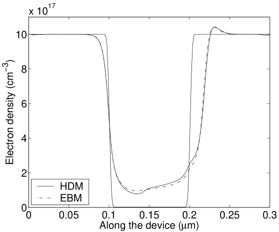
Fig. 1 shows the electron density for the EB and HD charge transport models for a bias of 1 V. The choice of 1 V is meaningful since at higher bias ( V), the HDM would no longer be applicable or the device would even be destroyed.
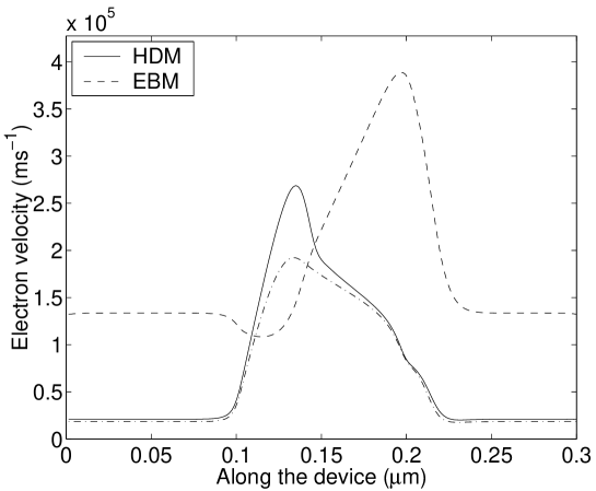
In this paper, solid lines refer always to the HDM anddashdotted lines to the EBM. The HDM exhibits more structure than the EBM. It is interesting to observe that the electron flow becomes supersonic at m in the HDM (whereas it remains subsonic in the DDM). Fig. 2 shows also the soundspeed in the electron gas calculated from the electron temperature in the HDM, which is given by if heat conduction is included and by otherwise (dashed curve). In fact, a shock wave develops in the region where the Mach number is greater than one. In the DDM, the electron velocity exceeds the saturation at most by 30%. The maximum electron velocity in the HDM is , in the EBM only .
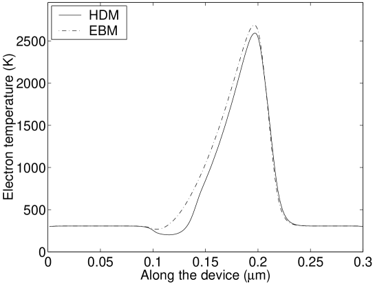
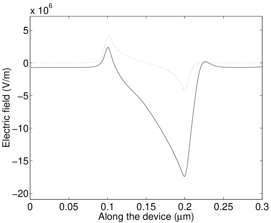
Finally we observe in Fig. 3 that the EBM is able to describe the electron temperature in an acceptable way. It also predicts the cooling of the electron gas near , which is caused by the little energy barrier visible in Fig. 4, where the electric field has a positive value. The dotted line in Fig. 4 show the electric field in thermal equilibrium.
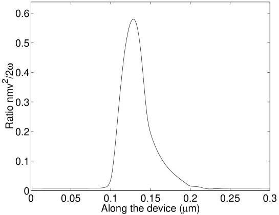
But still it is interesting to note that the drift part of the mean electron energy becomes large in a small region around the drain-source junction, where the electron kinetic energy can be as large as 58% of the total energy (Fig. 5).
From the point of view of device modeling, the J-V-characteristics resulting from the three models is of importance (Fig. 6). At low bias, the electron mobility is in all three models is governed by the low field mobility .
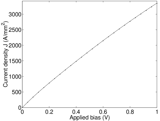
But it is quite astonishing how the EBM predicts a J-V-curve which is in very good agreement with the HDM prediction also in the range of higher biases, such that the two curves in Fig. 6 are nearly undistinguishable. As we have already mentioned, the EBM does not take inertia effects into account, which play no role for the stationary case. The predictive power of the two models is quite different, as we will see in the next section. But in the stationary case, the difference in the J-V-characteristics is, roughly speaking, averaged out.
5 Inertia effects
For GaAs, the relaxation times are quite high. Therefore, inertia effects will become important if the applied electric field changes at a high frequency. We simulated therefore a GaAs ballistic diode at 300 K. The diode begins with an m source region with doping density , is followed by an m n channel region (), and ends with an m drain region (). The relevant data like energy-dependent relaxation times and electron mass were obtained by two-valley MC simulations, where also the non-parabolicity of the two lowest conduction band valleys in GaAs was taken into account. For the sake of brevity we will not go into details here, which will be given in a forthcoming paper concerning the full hydrodynamic simulation of a GaAs MESFET structure.
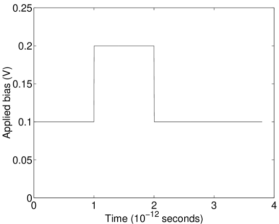
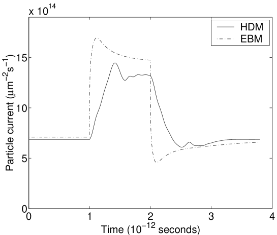
In order to show the different behavior of the HDM and EBM in time-domain, we applied to the 0.1 V pre-biased ballistic diode an additional 0.1 V pulse of 1 picosecond duration (see Fig. 7). Fig. 8 shows the particle current density in the exact middle of the device for both models as a function of time. Whereas the current in the EBM reacts immediately to the applied field, the current in the HDM shows relaxation effects. The impulse relaxation time in the channel of the diode is of the order of 0.3 picoseconds, the energy relaxation time lies between 0.3 and 1 picosecond. We emphasize the fact that considering the total current
| (41) |
does not help; the effect remains. Therefore we must conclude that the EBM, which is often termed ”hydrodynamic model” in commercial semiconductor device simulators, may lead accidentally to reasonable (static) characteristics of a device, although the physical processes inside the device are modelled incorrectly.
6 Conclusion
A simple discretization scheme for the hydrodynamic model is given in full detail which gives a valuable tool to the practitioner entering the field of hydrodynamic device modeling. Comparisons of the different transport models show that the energy-balance model is capable of describing the behavior of submicron devices fairly well, but full hydrodynamic simulations are needed in order to give a satisfactory description of the device from the physical point of view. At high frequencies, inertia effects become important in GaAs and related materials. It is therefore clear that the EBM will be no longer adequate for simulation of high-speed submicron devices in the near future.
References
- [1] K. Tomizawa, Numerical simulation of submicron semiconductor devices. Artech House: London, Boston, 1993.
- [2] K. Blotekjaer,”Transport equations for electrons in two-valley semiconductors,” IEEE Trans. Electron Dev., vol. 12, pp. 38-47, 1970.
- [3] D.M. Caughey, R.E. Thomas, ”Carrier mobilities in silicon empirically related to doping and field,” IEEE Proc., vol. 55, pp. 2192-2193, 1967.
- [4] Y.K. Feng, A. Hintz, ”Simulation of submicrometer GaAs MESFETs using a full dynamic transport model,” IEEE Trans. Electron Dev., vol. 35, pp. 1419-1431, 1988.
- [5] M.A. Alsunaidi, S.M. Hammadi, S.M. El-Ghazaly, ”A parallel implementation of a two-dimensional hydrodynamic model for microwave semiconductor device including inertia effects in momentum relaxation,” Int. J. Num. Mod.: Netw. Dev. Fields, vol. 10, pp. 107-119, 1997.
- [6] G. Baccarani, M.R. Wordemann, ”An investigation of steady-state velocity overshoot in silicon,” Solid-State Electron., vol. 28, pp. 407-416, 1985.
- [7] A. Gnudi, F. Odeh, M. Rudan, ”Investigation of nonlocal transport phenomena in small semiconductor devices,” European Transactions on Telecommunications and Related Technologies, vol. 1, no.3, pp. 307-312, 1990.
- [8] C. Canali, C. Jacoboni, G. Ottaviani, A. Alberigi Quaranta, ”High-field diffusion of electrons in silicon,” Appl. Phys. Lett., vol. 27, pp. 278-280, 1975.
- [9] D.L. Scharfetter, H.K. Gummel, ”Large-signal analysis of a silicon Read diode oscillator,” IEEE Trans. Electron Dev., vol. 16, no.1, pp. 64-77, 1969.
- [10] T. Tang, ”Extension of the Scharfetter-Gummel algorithm to the energy balance equation,” IEEE Trans. Electron Dev. 1984, vol. 1, no. 12, pp. 1912-1914, 1984.
- [11] C.L. Gardner, ”Numerical simulation of a steady-state electron shock wave in a submicrometer semiconductor device,” IEEE Trans. Electron Dev., vol. 38, pp. 392-398, 1991.
Biographies
Andreas Aste received the diploma degree in theoretical physics from the University of Basel, Basel, Switzerland, in 1993, and the Ph.D. degree from the University of Zürich, Zürich, Switzerland, in 1997. From 1997 to 1998 he was a post doctoral assistant at the Institute for Theoretical Physics in Zürich. From 1998 to 2001 he was a research assistant and Project Leader in the Laboratory for Electromagnetic Fields and Microwave Electronics of the Swiss Federal Institute of Technology ETH. Since 2001 he is working as a researcher at the Institute for Theoretical Physics at the University of Basel.
Dr. Aste is a member of the American Physical Society APS.
Rüdiger Vahldieck received the Dipl.-Ing. and Dr.-Ing. degrees in electrical engineering from the University of Bremen, Germany, in 1980 and 1983, respectively. From 1984 to 1986, he was a Research Associate at the University of Ottawa, Ottawa, Canada. In 1986, he joined the Department of Electrical and Computer Engineering, University of Victoria, British Columbia, Canada, where he became a Full Professor in 1991. During Fall and Spring 1992-1993, he was visiting scientist at the Ferdinand-Braun-Institute für Hochfrequenztechnik in Berlin, Germany. Since 1997, he is Professor of field theory at the Swiss Federal Institute of Technology, Zürich, Switzerland. His research interests include numerical methods to model electromagnetic fields in the general area of electromagnetic compatibility (EMC) and in particular for computer-aided design of microwave, millimeter wave and opto-electronic integrated circuits.
Prof. Vahldieck, together with three co-authors, received the 1983 Outstanding Publication Award presented by the Institution of Electronic and Radio Engineers. In 1996, he received the 1995 J. K. Mitra Award of the Institution of Electronics and Telecommunication Engineers (IETE) for the best research paper. Since 1981 he has published over 170 technical papers in books, journals and conferences, mainly in the field of microwave computer-aided design. He is the president of the IEEE 2000 International Zürich Seminar on Broadband Communications (IZS’2000) and President of the EMC Congress in Zürich. He is an Associate Editor of the IEEE Microwave and Wireless Components Letters and a member of the Editorial Board of the IEEE Transaction on Microwave Theory and Techniques. Since 1992, he serves also on the Technical Program Committee of the IEEE International Microwave Symposium, the MTT-S Technical Committee on Microwave Field Theory and in 1999 on the Technical Program Committee of the European Microwave Conference. He is the chairman of the IEEE Swiss Joint Chapter on IEEE MTT-S, IEEE AP-S, and IEEE EMC-S.