Spatiotemporal patterns in a DC semiconductor-gas-discharge system:
Stability analysis and full numerical solutions
Abstract
A system very similar to a dielectric barrier discharge, but with a simple stationary DC voltage, can be realized by sandwiching a gas discharge and a high-ohmic semiconductor layer between two planar electrodes. In experiments this system forms spatiotemporal and temporal patterns spontaneously, quite similarly to e.g., Rayleigh-Bénard convection. Here it is modeled with a simple discharge model with space charge effects, and the semiconductor is approximated as a linear conductor. In previous work, this model has reproduced the phase transition from homogeneous stationary to homogeneous oscillating states semiquantitatively. In the present work, the formation of spatial patterns is investigated through linear stability analysis and through numerical simulations of the initial value problem; the methods agree well. They show the onset of spatiotemporal patterns for high semiconductor resistance. The parameter dependence of temporal or spatiotemporal pattern formation is discussed in detail.
pacs:
05.45.–a, 52.80.–s, 47.54.–r, 02.60.CbI Introduction
I.1 Experiments and observations
Spontaneous pattern formation is a general feature in the natural and technical sciences in systems far from equilibrium Cross . It is a fascinating phenomenon, but can also be detrimental when homogeneity and stationarity are required in a technical process. Pattern formation occurs frequently in gas discharges, like in dielectric barrier discharges Kogel1 ; Kogel2 that are used, e.g., for ozone production and in plasma display panels. It is therefore both fundamentally interesting and technically relevant to understand the mechanisms and conditions of spontaneous symmetry breaking in such systems.
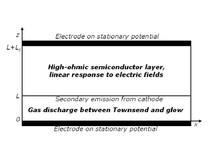
A dielectric barrier discharge system consists of a layered structure that in the simplest case consists of a planar electrode, a dielectric layer, a gas discharge layer, and another planar electrode Kogel1 ; Kogel2 . To the outer electrodes, an AC voltage is applied that forces the system periodically in time. In the present paper, an even simpler physical system will be analyzed: a system with essentially the same set-up, but with a DC voltage supply, i.e., a stationary drive. The system is illustrated in Fig. 1. To allow current to flow with the DC drive, the dielectric layer is replaced by a high-Ohmic semiconductor.
Independently of the above technical applications, both the AC and the DC system have attracted much attention in the pattern formation community in the past two decades, since they are easy to operate, have convenient length and time scales and a wealth of spontaneously created spatio-temporal patterns. When the transversal extension of the layers is large enough, experiments show homogeneous stationary and oscillating modes, and patterns with spatial and spatio-temporal structure like stripes, spots, and spirals Willebrand ; Gwinn ; Str1 ; Str2 ; Str3 ; Str4 ; StrTh ; Astr1 ; Astr2 ; Astr3 ; Astr4 ; Astr5 ; Astr6 ; Astr7 ; Astr8 ; Astr9 . The aspect ratio of a thin layer with wide lateral extension and the observation from above are reminiscent of Rayleigh-Bénard convection as the classical pattern forming system in hydrodynamics.
The experiments on DC driven ”barrier” discharges in Ref. Str1 ; Str2 ; Str3 ; Str4 ; StrTh describe not only phenomena at one particular set of parameters, but in Str2 ; StrTh also explore parameter space and draw phase diagrams for the transition between different states; therefore we concentrate on those — we are not aware of other experimental investigations of such phase diagrams. The experiments Str2 ; StrTh are performed on a nitrogen discharge at 40 mbar in a gap of 1 mm. The semiconductor layer consists of 1.5 mm of GaAs. The applied voltages are in the range of 580 V to 740 V. Through photosensitive doping, the conductivity of the semiconductor layer can be increased by an order of magnitude; the dark conductivity is . These parameters imply that the product of pressure and distance of the gas discharge is short, but still sufficiently far on the right hand side of the Paschen curve that the transition from Townsend to glow discharge is subcritical, i.e., that the voltage at stationary operation drops when the current rises. The resistance of the semiconductor together with the applied voltage constrain the operation to this transition regime from Townsend to glow discharge. The system forms stationary states of the discharge that are homogeneous in the transversal direction, as well as spontaneously oscillating states that still are spatially homogeneous and also oscillating states that show spatial patterns in the transversal directions as well. In mathematical terms, the last two states emerge from the homogeneous stationary state through a Hopf-bifurcation (leading to spontaneous oscillations) or through a Turing-Hopf-bifurcation (leading to spatial and temporal structures). While we investigated the Hopf-bifurcation in previous work first ; second , we here include possible structures in the transversal direction and analyze the occurrence of Turing-, Turing-Hopf- and Hopf-bifurcations.
I.2 Theoretical approaches and understanding
Theoretical studies both of the DC and of the AC driven barrier discharge are few; they basically fall into two classes: simulations or reduced 2D reaction-diffusion models. Simulations can only be carried out for particular parameter sets; for these parameters, physical mechanisms of pattern formation can be identified and visualized. Reaction-diffusion models Willebrand ; fronts ; RGM in the transversal 2D plane can be investigated analytically, but their derivation from the full 3D physical model depends on ad hoc approximations whose range of validity beyond the linear regime fronts of the Townsend discharge remains unclear.
In previous first ; second and in the present work, we have chosen a third line of theoretical investigation. Namely, we investigate the linear stability of the homogeneous stationary state and identify the physical nature of the fastest growing destabilization modes. This allows us to derive complete phase transition diagrams. This approach is used in many branches of the sciences, but has been little explored in gas discharges. The stability analysis gives a clue for interesting parameter regimes that can be further investigated by simulations.
In more physical detail, the state of theoretical understanding and simulations is summarized as follows.
First, for the AC system, the importance of surface charges deposited on the discharge boundaries in each half-cycle of the voltage drive was identified in Gwinn and elaborated in Ingo1 ; Ingo2 ; ChinaAC . Simulations use the same fluid models with self generated electric fields as simulations of plasma display panels Punset , most work is performed in two spatial dimensions. Fully three dimensional simulations have recently been performed in 3DAC . These simulations are in reasonable agreement with experimental results, given the uncertainty of the microscopic parameters in the discharge models. Note that even in the 2D system, simulations do not cover many periods of the AC drive, typically not more than 20; therefore, they have to start from initial conditions fairly close to the final state and cannot follow intermediate transients in detail.
For the simpler DC driven system, we are not aware of studies of the full discharge model coupled to the high-Ohmic semiconductor layer, except for a reaction-diffusion model of the system in the two transversal directions, that is developed, e.g., in Astr9 ; fronts ; as said above, this approach does not appropriately resolve the dynamics in the direction normal to the layers. Of course, surface charges on the gas-semiconductor interface again have to play a role like in the AC system, as the electric field can be discontinuous across the interface first ; second ; fronts . But a full model needs to account for space charges and ion travel times in the bulk of the gas discharge as well, cf. first ; second .
In our previous work first ; second , we concentrated on the purely temporal oscillations that occur in a spatially homogeneous mode, therefore the analysis was restricted to the direction normal to the layers, assuming homogeneity in the transversal direction. The results presented in first showed that a simple two-component reaction-diffusion approximation for current and voltage in the gas discharge layer is not sufficient to describe the oscillations, though such a model is suggested through phenomenological analogies with pattern forming systems like Belousov-Zhabotinski reaction, Rayleigh-Bénard convection, patterns in bacterial colonies etc. In second , we predicted the phase transition diagram from a homogeneous stationary to a homogeneous oscillating state. These predictions were in semi-quantitative agreement with the experiments described in Str2 .
I.3 Questions addressed in this paper
Here we investigate the spontaneous emergence of spatio-temporal patterns in DC driven systems, and predict in which parameter regimes pattern formation can be expected. While our previous work dealt with the stationary solutions Dana ; RES or the dynamics in the single direction normal to the layers first ; second , now the transversal direction is included into analysis and simulations as well. The experiments described in the paper Str2 and thesis StrTh systematically explore the parameter dependence of pattern formation in the system, and we do the same, but theoretically. The system in Str2 never forms modes that are only spatially structured, but stationary, i.e., it never undergoes a pure Turing transition. Rather, starting from a homogeneous stationary state, either the homogeneous oscillating state from second is reached through a Hopf-bifurcation, or a spatially structured time-dependent state through a Turing-Hopf-bifurcation. Furthermore, for high semiconductor resistivity, typically a spatially structured oscillating state is reached while for low resistivity, the oscillating structures are homogeneous in the transversal direction. Within the present paper we investigate these transitions first through linear stability analysis; furthermore interesting parameters regimes are investigated through simulations as well. We use a fluid model for gas discharge and semiconductor layer coupled to the electrostatic Poisson equation; in the gas discharge model electrons are adiabatically eliminated to reduce computational costs.
The paper is organized as follows. In Sec. II we introduce the model, perform dimensional analysis, and reduce the model by adiabatic elimination of electrons. In Sec. III, the problem of linear stability analysis of the homogeneous stationary state is formulated, the equations are rewritten and numerical solution strategies are discussed. Sec. IV contains the results of the stability analysis, first the qualitative behavior of the dispersion relation as a function of the transversal wave number , and then predictions on the parameter dependence of the dispersion relations. Sec. V presents numerical solutions of the full initial value problem and a comparison with the stability analysis results; they reveal that both methods can be trusted. Finally, Sec. VI contains discussion and conclusions. The numerical details for the solution of the full p.d.e. system are given in the appendix.
II The Model
In this section, the simplest model for the full two-dimensional glow discharge–semiconductor system is introduced. Its schematic structure is shown in Fig. 1. For the gas discharge, it contains electron and ion drift in the electric field, bulk impact ionization and secondary emission from the cathode as well as space charge effects. The semiconductor is approximated with a constant conductivity. The same physics was previously studied, e.g., in Engel ; Raizer and in our previous papers Dana ; RES ; first ; second . However, in these previous papers, any pattern formation in the transversal direction was excluded and only the single dimension normal to the layers was resolved. The model then only allows for stationary solutions Dana ; RES or temporal oscillations first ; second . We now study the onset of patterns in the direction parallel to the layers. If the layers are laterally sufficiently extended, there is rotation and translation invariance within the plane. Linear perturbations can then be decomposed into Fourier modes. These Fourier modes can be studied in a two-dimensional setting, i.e., in one direction normal and one direction parallel to the layers. They are the subject of the paper.
II.1 Gas-discharge and semiconductor layers
The gas-discharge part of the model consists of continuity equations for two charged species, namely, electrons and positive ions with particle densities and :
| (1) | |||||
| (2) |
which are coupled to Poisson’s equation for the electric field in electrostatic approximation:
| (3) |
Here, is the electric potential, is the electric field in the gas discharge, is the elementary charge, and is the dielectric constant. The vector fields and are the particle current densities, that in simplest approximation are described by drift only. In general, particle diffusion could be included, however, diffusion is not likely to generate any new structures, but rather to smoothen out the structures found here. The drift velocities are assumed to depend linearly on the local electric field with mobilities :
| (4) |
hence the electric current in the discharge is
| (5) |
Two types of ionization processes are taken into account: the process of electron impact ionization in the bulk of the gas, and the process of electron emission by ion impact onto the cathode. In a local field approximation, the process determines the source terms in the continuity equations (1) and (2):
| (6) |
We use the classical Townsend approximation
| (7) |
The gas discharge layer has a thickness , where subscripts or refer to gas or semiconductor layer, respectively. The semiconductor layer of thickness is assumed to have a homogeneous and field-independent conductivity and dielectric constant :
| (8) |
The space charge density inside the semiconductor with constant conductivity is assumed to vanish.
II.2 Boundary conditions
In dimensional units, parametrizes the direction parallel to the layers, and the direction normal to them. The anode of the gas discharge is at , the cathode end of the discharge is at , and the semiconductor extends up to . (Below, in dimensionless units, this corresponds to coordinates and .)
When diffusion is neglected, the ion current and the ion density at the anode vanish. This is described by the boundary condition on the anode :
| (9) |
The boundary condition at the cathode, , describes the -process of secondary electron emission:
| (10) | |||||
Across the boundary between gas layer and semiconductor layer, the electric potential is continuous while the discontinuity of the normal electric field is determined by the surface charge
| (11) |
where is the normal vector on the boundary, directed from the gas toward the semiconductor, i.e., in the direction of growing . The change of surface charge in every point of the line is determined by the electric current densities in the adjacent gas and semiconductor layers as
| (12) |
where and are the current densities at in gas and semiconductor. is given in Eq. (8), on the boundary due to condition (10) is
| (13) |
Equations (11)–(13) are summarized as
This boundary condition is valid in any point of the gas-semiconductor boundary .
Finally, a DC voltage is applied to the gas-semiconductor system determining the electric potential on the outer boundaries
| (15) |
Here the first potential vanishes due to gauge freedom.
II.3 Dimensional analysis
The dimensional analysis is performed essentially as in first ; second ; saarlos ; Dana ; RES . However, as it is useful to measure the time in terms of the ion mobility rather than the electron mobility, we introduce the intrinsic parameters of the system as
| (16) |
Here time immediately is measured in units of , while in second , first the time scale was used. The intrinsic dimensionless parameters of the gas discharge are the mobility ratio of electrons and ions and the length ratio of discharge gap width and impact ionization length:
| (17) |
The dimensionless time, coordinates and fields are
| (18) |
Here the dimensional is expressed by coordinates and the dimensionless by .
The total applied voltage is rescaled as
| (19) |
The dimensionless parameters of the semiconductor are conductivity and width :
| (20) |
Note that the dimensionless conductivity is now also measured on the scale of ion mobility. Dimensionless capacitance and resistance of the semiconductor and its characteristic relaxation time are expressed in terms of these quantities as
| (21) |
II.4 Adiabatic elimination of electrons and final formulation of the problem
The dynamics of a glow discharge takes place through ion motion where the ions are much slower than the electrons. As in second , the electrons therefore equilibrate on the time scale of ion motion and can hence be adiabatically eliminated: After substituting , the gas discharge part of the system has the form
| (22) | |||||
| (23) | |||||
| (24) |
and in the limit of , it becomes
| (25) | |||||
| (26) | |||||
| (27) |
As in second , the electric field is now only influenced by the ion density , and not by the much smaller density of fast electrons (since the electrons are generated in equal numbers, but leave the system much more rapidly), and the electrons follow the ion motion instantaneously: given the electron density on the cathode and the field distribution in the gas gap, the electron density is determined everywhere through (25). The boundary conditions (9) and (10) for electrons and ions are
| (28) |
After rescaling, the semiconductor is written as
| (29) |
and the condition (II.2) for the charge on the semiconductor-gas boundary becomes
| (30) | |||
In the perturbation analysis, the differential form of charge conservation on the boundary is used
| (31) |
The total width of the layered structure is . On its outer boundaries and , the electrodes are on the electric potential and , respectively. Finally, in the numerical solutions of the PDEs, lateral boundaries at and with periodic boundary conditions for , , and are introduced.
II.5 Parameter regime of the experiments
The parameters are taken as in the experiments Str2 ; StrTh and in our previous work second . The discharge is in nitrogen at 40 mbar in a gap of 1 mm. The semiconductor layer consists of 1.5 mm of GaAs with dielectric constant . The applied voltages are in the range of 580–740 V. Through photosensitive doping, the conductivity of the semiconductor layer could be increased by an order of magnitude; the dark conductivity was .
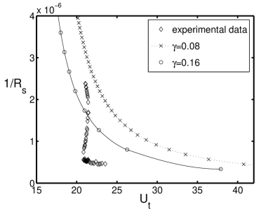
For the gas discharge, we used the ion mobility and electron mobility , therefore the mobility ratio is . For and for , we used values from Raizer . The secondary emission coefficient was taken as . (Comparison with experiment in second as reproduced in Fig. 3 below might suggest , but that seems unreasonably large.) Therefore the intrinsic scales from (16) are
| (32) | |||||
the gas gap width of mm corresponds to in dimensionless units, and the semiconductor width of mm to a dimensionless value of . The dimensionless applied voltages are in the range of , which correspond to the dimensional range of . The dimensionless capacitance of the semiconductor is . We investigate the conductivity range of which corresponds to a semiconductor resistance of 700 to 7000 in the new dimensionless units (or to to in the units of our previous papers first ; second ).
For the lowest conductivity of , pattern formation consistently occurs neither in our analysis nor in the experiment; this case is not discussed further in this paper.
II.6 Experiment: between Townsend and glow
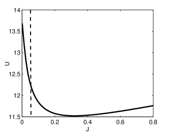
The parameter regime of the experiments Str2 ; StrTh as discussed above can now be placed in the transition regime between Townsend and glow discharge as follows. We recall Dana ; RES that the stationary voltage of the space charge free Townsend regime is minimal at a discharge length of , which is for or for example for . ( is known as the Paschen curve.) Continuing with in the remainder of the paper, the transition from Townsend discharge to the space charge dominated glow discharge is purely subcritical, i.e., the current-voltage characteristic is falling, if the discharge is longer than ; this is here the case. In fact, for the experimental value and , the Townsend voltage is , while the minimum of the voltage in the glow regime is , it is reached at a current of as shown in figure 2. In the experiment the applied voltage does not exceed , and the resistance of the semiconductor is at least , this situation is indicated as the dashed load line in figure 2. Therefore the current in the stationary homogeneous mode does not exceed 0.07, i.e., it stays in the transition region between Townsend and glow regime.
III Stability analysis: Method
In this section, the stability analysis of the homogeneous stationary state is set up. While in earlier work second , only temporal oscillations were admitted, here the stability with respect to temporal and spatial perturbations is analyzed. In particular, linearized equations are derived that define an eigenvalue problem, and the numerical solution strategy is discussed. It becomes particularly demanding for large wave numbers . The method developed in this chapter forms the basis for the derivation of dispersion relations in Chapter IV.
III.1 Linear perturbation analysis for transversal Fourier modes: problem definition
Here the equations are derived that describe linear perturbations of the stationary state that is furthermore homogeneous in the transversal direction, in agreement with the external boundary conditions. The analysis is set up as in second , but now also transversal perturbations are admitted. The unperturbed equations are denoted by a subscript 0, they are for
| (33) | |||||
| (34) | |||||
| (35) |
with boundary conditions
| (36) | |||||
Here is the total current and is the applied voltage. For a further discussion, see Dana ; RES ; second .
The first order perturbation theory is denoted by a subscript 1. As the transversal modes can be decomposed into Fourier modes with wavenumber within linear perturbation theory, the ansatz
| (37) | |||
| (38) | |||
| (39) |
is used where the perturbation is supposed to be small. Insertion of this ansatz into the equations for the gas discharge (25)–(27) yields
| (42) | |||||
| (43) |
Here is the field perturbation in the direction. The boundary conditions are:
| (44) |
where is the boundary between gas discharge and semiconductor layer.
In the semiconductor layer, the equation with the boundary condition at the position of the cathode has to be solved. For , this means that we have to solve with . This problem is solved explicitly for by
| (45) |
with the arbitrary coefficient . The ’jump’ condition (30), (31) for the electric field on the semiconductor gas discharge boundary is expressed as
| (46) |
after is eliminated. As the potential (45) is continuous we get on the boundary of the gas discharge region
| (47) |
Now in (III.1) can be substituted by through (47). The result is the second boundary condition at
| (48) |
Now the semiconductor is integrated out, and we are left with four first order ordinary differential equations (III.1)–(43) and four boundary conditions (44), (48) that together determine an eigenvalue problem for .
III.2 New fields lead to compacter equations
It is convenient to write the equations (III.1) in terms of the fields and
| (49) |
as in second . Furthermore, for non-vanishing wave-numbers , it is convenient to use charge conservation
| (50) |
to eliminate particle densities completely in favor of the component of the total current density
| (51) |
This leads to a compacter form of the system (III.1)–(43):
| (52) | |||||
| (53) | |||||
| (54) | |||||
| (55) |
The boundary conditions (44) and (48) are rewritten as:
| (56) | |||||
| (57) | |||||
| (58) | |||||
| (59) |
Note that in the last equation, the identity was used. Note further that the limit of of these equations reproduces the limit of of the analogous 1D equations in second .
III.3 Formal solution and numerical implementation
In matrix form, the linearized equations (52)–(55) are
| (64) | |||
| (69) |
The matrix depends on wavenumber and eigenvalue and total current . It depends on through the functions , , and .
The boundary conditions (56), (57) at mean that the general solution of the linear equation can be written as a superposition of two independent solutions of (64)
| (78) |
The solution (III.3) has to obey the boundary conditions (58) and (59) at as well. Denoting the components of the solutions as for , we get
| (79) | |||
| (80) |
These equations have nontrivial solutions, if the determinant
| (81) | |||
| (84) |
vanishes at
| (85) |
Now for a fixed , we start with some initial estimate for the eigenvalue and solve equation (III.3) numerically for both initial values. The next estimate for can be found from condition (85) since it is quadratic in . This process is iterated until the accuracy is sufficient. We used the condition for the ’th iteration step to finish iterations. For the stability of the iteration process under-relaxation was used. For the integration of the equations (64), we used the classic fourth-order Runge-Kutta method on a grid with 500 nodes. The majority of investigated solutions of the present problem are oscillating, therefore the eigenvalues are complex, and the eigenfunctions are complex as well. We have taken this into account by working with complex fields.
After the eigenvalue is found, the eigenfunction is determined by inserting the ratio
| (86) |
into Eq. (III.3).
III.4 Numerical strategy for large
The above method gives reliable results for small values of and has been used to derive the results presented in Sect. IV.2. However, for investigating possible instabilities for large wave number as in Sect. IV.1, e.g., for finding both solution branches for in Fig. 4, a better strategy is needed.
There are two points where the integration routine has to be improved for large . There is first the fact that the matrix of coefficients is poorly conditioned. This can be seen by noting that one column is much bigger than another one. A more precise measure of numerical ill-conditioning of a matrix is provided by computing the normalized determinant of the matrix. When the normalized determinant is much smaller than unity, the matrix is ill-conditioned. The normalized determinant is obtained by dividing the value of the determinant of the matrix by the product of the norms of the vectors forming the rows of the matrix.
The second point is the so-called ‘build-up’ error. The difficulty arises because the solution (III.3) requires combining numbers which are large compared to the desired solution; that is and can be up to 3 orders of magnitude larger than their linear combination, which is the actual solution. Hence significant digits are lost through subtraction. This error cannot be avoided by a more accurate integration unless all computations are carried out with higher precision. Godunov Godunov proposed a method for avoiding the loss of significance which does not require multi-precision arithmetics and which is based on keeping the matrix of base solutions orthogonal at each step of the integration.
A modification of Godunov’s method Conte , which is computationally more efficient and which yields better accuracy, is implemented in the algorithm used for large . The main difference to the algorithm described in Section III.3 is that here we examine the base solutions (obtained by any standard integration method) at each mesh point and when they exceed certain nonorthogonality criteria we orthonormalize the base solution. We have to start with initial conditions that are orthogonal to each other and not only to the boundary conditions:
| (91) | |||||
| (96) |
| (97) |
Based on the orthogonalization developed in Conte , the differential equation (64) can be solved very accurately even for large , which allows us to find the eigenvalues according to the criteria described in the previous section.
Since we must solve the matrix equation (64) several times for different values of , we must insist that the orthonormalization is the same for all these solutions. In essence we must insist that the determinant is uniformly scaled in order for the successive approximations for to be consistent. Numerically this can be accomplished by determining the set of orthonormalization points and matrices for the solution corresponding to the first initial guess for and thereafter applying the same matrices at the corresponding points for all successive solutions.
The program is written in C, and the integration method is one-step simple Runge-Kutta and on the domain L=36 the number of grid points is varied from n=500 to n=18000 depending on the range of .
IV Stability analysis: dispersion relations
Having set the mathematical basis for the stability analysis, now dispersion relations and bifurcation diagrams can be derived and discussed. In previous work second , we have analyzed pure Hopf transitions where the homogeneous stationary state becomes unstable to homogeneous oscillations. The bifurcation diagram for the Hopf transition for the experimental parameters described in Sections II.5 and II.6 is shown in Fig. 3, it is reproduced from Fig. 11 in second . Any structures in the transversal direction were excluded in this earlier work. We now take this diagram as a basis and investigate which additional spatial or spatio-temporal instabilities can occur.
IV.1 Hopf or Turing-Hopf bifurcations
If patterns form spontaneously in the system due to a linear instability, i.e., in a supercritical bifurcation, its signature will be found in the dispersion relation . More precisely, there will be a band of Fourier modes with positive growth rate Re . If the instability is purely growing or shrinking without oscillations, i.e., if Im , it is called a Turing instability. On the other hand, if the imaginary part of the dispersion relation does not vanish (Im ), the system oscillates. If the most unstable mode has no spatial structure, , but only oscillates, we speak of a Hopf transition, while if , the transition is called Turing-Hopf.
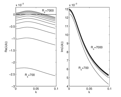
For three values of , namely for 700, 1400 and 7000, the dependence of the dispersion relation on the applied voltage was investigated.
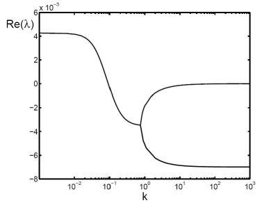
IV.1.1 Qualitative behavior for and 1400
For , a generic shape of the dispersion relation is presented in Fig. 4. Here a very large range of values is shown on a logarithmic scale. The point on the axis was previously treated in second . The dispersion curves extend continuously from to small : there is a pair of complex conjugate eigenvalues that is represented by the single line for Re. For of order unity, the two complex conjugate solutions in Fig. 4 merge and form two solutions with different real part and vanishing imaginary part.
The dynamic behavior is typically dominated by the mode with the largest positive growth rate Re. If the growth rate is negative for all , the system is dynamically stable. Here the mode with the largest growth rate has vanishing wave number and nonvanishing Im ; therefore we expect a Hopf bifurcation towards oscillating homogeneous states. If the upper solution in Fig. 4 would develop a positive growth rate for large , we had found an exponentially growing, purely spatial Turing instability at short wave lengths, but we haven’t found such behavior.
Variation of the applied voltage leads to the same qualitative behavior: the temporally oscillating, but spatially homogeneous mode has the largest growth rate. Whether this maximal growth rate is positive or negative, can be read from Fig. 3. The behavior for is qualitatively the same.
IV.1.2 Qualitative behavior for
Further increase of the semiconductor resistivity to creates a new feature, namely a Turing-Hopf-instability: the growth rate becomes maximal for some non-vanishing, but very small value of , as can be seen in Fig. 5.
In Fig. 6, real and imaginary part of the two largest eigenvalues are plotted for a larger range of . Up to , a pair of complex conjugate eigenvalues is found, then two different branches of purely real eigenvalues emerge, similarly to the behavior for smaller in Fig. 4.
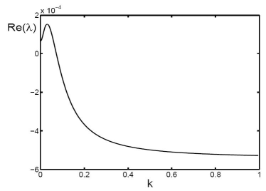
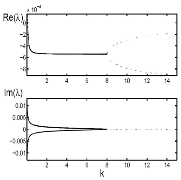
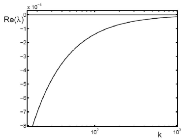
Finally, Fig. 7 shows that the most unstable branch of eigenvalues approaches Re from below for , but does not develop any positive growth rate. Growth rates for large always stayed negative when exploring the parameters of the system numerically. If positive growth rates would exist, they would indicate a purely growing spatial mode with very short wave length.
IV.1.3 Quantitative predictions
The above observations are now quantified in Figure 8. It shows how the most unstable wave number and real and imaginary part of the corresponding eigenvalue depend on the feeding voltage at different dimensionless resistances , 1400 and 7000. The curves begin where the applied voltage equals the Townsend breakdown voltage 13.7, cf. Section II.6.
Panel (a) shows that for small the most unstable wavelength is always non-vanishing, and that it decreases for growing until it vanishes at some critical . Panel (b) shows that the growth rate Re of the most unstable mode can stay negative in the whole range where . This explains why the finite wave length instabilities were not seen above for small . Panel (c) shows that the most unstable modes are always oscillating in time.
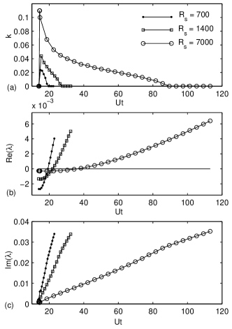
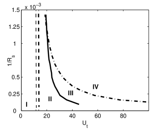
These results are further summarized in Figure 9 which is the counterpart of Fig. 3, but with , i.e., with the definition of of the present paper. The solid line in Fig. 9 is the line where Re changes sign. This line is essentially identical with the solid line in Fig. 3 that denotes the sign change of Re . The dash-dotted line denotes where the most unstable wave number vanishes. The dashed lines denote the voltage of the Townsend and the glow discharge.
The figure shows a calculated bifurcation diagram: In region I, a discharge cannot form, in region II, the homogeneous stationary discharge is stable, in region III, it is Turing-Hopf-unstable, and in region IV, it is Hopf-unstable.
IV.1.4 Comparison with experiments
Comparing this calculated bifurcation diagram with the experimental one in Str2 ; StrTh , there is one point in common and one differs.
The common point is that there are no purely spatial patterns without oscillations in the experiment, in agreement with the theoretical prediction that there is no pure Turing instability. Furthermore the transition from stationary to oscillating states occurs roughly in the same parameter regime, cf. Fig. 3. The oscillations are due to the following cycle: the voltage on the gas discharge is above the Townsend value and the ionization in the discharge increases, the discharge deposits a surface charge on the gas-semiconductor interface hence reducing the voltage on the discharge and eventually extinguishing it, the high resistance of the semiconductor leads to a long Maxwell relaxation time of the initial voltage distribution between gas and semiconductor, after which the cycle repeats.
The difference between experiment and calculation lies in the sequence of temporal and spatio-temporal patterns. In the experiments, for large conductivity on increasing first purely temporal and then spatio-temporal patterns are formed. For smaller , the system goes from stationary to oscillating and back to stationary behavior without loosing homogeneity. In our calculation, for large , the system directly transits from homogeneous stationary to homogeneous oscillating, while for small there is first a range of a Turing-Hopf-instability, and then a pure Hopf-instability takes over.
On this discrepancy, three remarks are in place. The nature of the linear instability of the homogeneous stationary system does not automatically predict the fully developed nonlinear pattern. Our spatial patterns have wave numbers typically much smaller than 0.1 which corresponds to wave lengths much larger than 60. Therefore our spatio-temporal instabilities do not correspond to the dynamic filaments described in Str2 , but rather to a range of diffuse moving bands. These diffuse moving bands occur before the blinking filaments discussed in Str2 ; they are only shortly described in the later Ph.D. thesis StrTh . We therefore suggest that the moving waves or bands can be identified with our predicted Turing-Hopf-instability, that creates running waves as well; the experimental data in StrTh do not allow a further comparison with theory and we therefore invite further experimental investigations. The authors of the experimental papers have suggested later Str4 ; Astr9 ; Mech that their experiment is more complex than our simple model due to nonlinearities in the semiconductor and in gas heating. Our calculation therefore shows that already this simple model exhibits Hopf- and Turing-Hopf-instabilities in the same parameter range.
IV.2 Dependence on gap lengths and resistance
We now investigate how the dispersion relations change when other system parameters are varied. While keeping material parameters for gas and semiconductor fixed, the following physical parameters can be varied: the widths and of the semiconductor and the gas layer, the externally applied voltage and the semiconductor resistance by a factor of 10 through photo-illumination. The dependence on was already discussed above; here the role of the other three parameters is investigated.
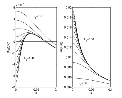
IV.2.1 Dependence on semiconductor width
In Fig. 10, we fixed the conductivity at its smallest value and varied from 10 to 150 in equal steps; resistance and capacitance then depend on like and according to equation (21) in section II.3. In physical units, the width of the semiconductor layer was changed from 0.28 mm to 4.17 mm. The length of the gas gap was . Rather than the total applied voltage , the current was fixed. For the value , the corresponding parameter values are , and as in Figs. 5, 6 and 7 above.
For small width the system shows a pure Hopf-instability (), but with increasing , the most unstable mode suddenly becomes nonvanishing, i.e., the system undergoes a first order transition to spatio-temporal patterns. Furthermore, the growth rates Re decrease and the oscillation frequencies Im increase when increases while the Maxwell relaxation time of the semiconductor does not vary.
For the smaller value , a similar behavior is observed: for the parameters of Fig. 4, there is still a Hopf bifurcation, but for increasing , the most unstable mode can become positive as well and a Turing-Hopf-instability occurs.
IV.2.2 Dependence on semiconductor resistance
Now the dependence on the conductivity of the semiconductor is tested that can be varied by illumination by a factor of 10. Accordingly, in Fig. 11, the resistance varies in the interval between 700 and 7000, while the other parameters are chosen as in the previous section: , , . The current is fixed; this value corresponds to a voltage of for . Therefore, the upper line in Fig. 11 is the same as the one in Figs. 5, 6 and 7.
For all values of the resistivity, the wave number where the growth rate Re is maximal, stays positive (), but it drops below zero for smaller making the homogeneous stationary state stable. Furthermore, for the smallest investigated , namely , and fixed , the voltage is , but when the growth rate is positive for the same range and has maximum for as can be seen in Fig. 4.
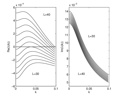
IV.2.3 Dependence on length of gas gap
Fig. 12 shows for the same parameter values that with increasing gas gap width , the growth rate increases and the oscillation frequency decreases, while the most unstable mode stays nonvanishing: . The explored gap lengths all correspond to a falling current voltage characteristics of the gas discharge, cf. section II.6.
V Numerical solutions of the initial value problem
V.1 Implementation and results
The full dynamical problem was also solved numerically as an initial value problem. This allows us to test the results of the stability analysis, to visualize the actual dynamics and also to study the behavior beyond the range of linear stability analysis. Details of the numerical implementation are given in the appendix.
We study the case of high resistivity that leads to spatial pattern formation as discussed above. Two values of the applied potential were investigated: where the homogeneous stationary state is stable, and where this state is Turing-Hopf-unstable.
In the transversal direction, we use periodic boundary conditions. We choose the lateral extension as a multiple of the most unstable wave length . After some tests with higher multiples showing essentially the same behavior, we used , i.e., the lateral extension is twice the expected wave length. The initial condition is
| (98) |
where is the wavenumber of the most unstable mode, is the stationary solution, and is the eigenfunction for constructed in Sect. III.3. The constant is chosen such that the perturbation is small compared to . Note that we need to specify the initial conditions for the ion density only, since electron density and field are determined instantaneously due to the adiabatic elimination of the fast electron dynamics.
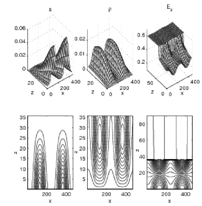
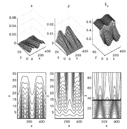
Figure 13 shows about one period of oscillation within 4 time steps for the pattern forming case (). For each instant of time, the rescaled electron density and the ion density are shown in the gas discharge region, and the electric field is shown both in the gas discharge and the semiconductor region, as will be discussed in more detail later. The upper row contains 3D plots and the lower row contour plots. The figures show the characteristic electron and ion distribution of a glow discharge, but with a strong spatio-temporal modulation.
The temporal period predicted by linear perturbation theory is 528. This is agrees approximately with the numerical results. On the other hand, the destabilization of the homogeneous stationary state in Fig. 13 is already far developed and in the fully nonlinear regime. Therefore the results of the stability theory at this time give only an indication for the full behavior. In particular, the nonlinearity has created an onset to doubling the spatial period that is absent for small perturbations.
![[Uncaptioned image]](/html/nlin/0608053/assets/x13.png)
![[Uncaptioned image]](/html/nlin/0608053/assets/x14.png)
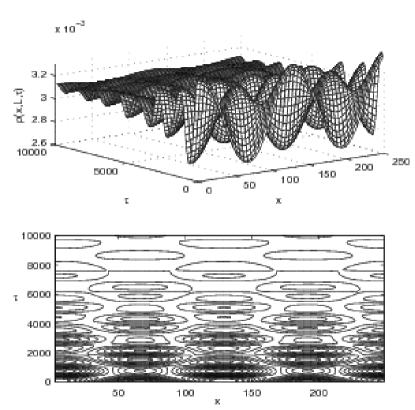
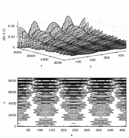
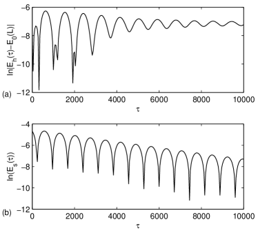
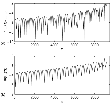
For presenting the evolution in time, the spatial structure has to be represented on a line rather than in the full -plane. Obviously, the ion density on the semiconductor-gas-interface is an appropriate quantity, since it characterizes the local intensity of the discharge glow in the transversal direction. Figures 14 and 15 show the complete temporal evolution in such a presentation. Fig. 14 presents data of a perturbation decaying towards the stationary homogeneous state for , while Fig. 15 shows the growing destabilization of the homogeneous stationary state for ; the late stage of this evolution was shown in Fig. 13.
V.2 Comparison of numerical and stability results
When one wants to compare results of the numerical simulation and of the stability analysis, the evolution of different spatial modes has to be extracted from the simulation. Appropriate quantities are the transversally averaged electric field on the gas-semiconductor interface
| (99) |
and the spatial modulation of the field
| (100) |
These quantities, or rather the logarithms of and of are shown for the stabilizing case in Fig. 16, and for the destabilizing case in Fig. 17.
In this logarithmic plot for the fields, the lines through the maxima are approximately straight, which means that the growth is exponential. For the destabilizing case, the growth rate of the spatial mode is slightly larger than that of the homogeneous mode which implies that the most unstable mode has a non-vanishing wave number : in agreement with linear stability analysis. Furthermore, at late stages when the dynamics is beyond the range of linear perturbation theory and becomes nonlinear, the growth of all modes accelerates.
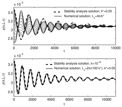
Figs. 18 and 19 show a quantitative comparison between stability analysis and computational results. Fig. 18 shows the stabilizing case . The stability analysis predicts that is the most unstable mode; it has the eigenvalue . Therefore, the period of the temporal oscillations is predicted as , the characteristic decay time as , and the characteristic wave length as . This predicted behavior is shown as the dashed line in the upper panel of Fig. 18. The solid lines show the numerical solution, more precisely the time evolution of the ion density evaluated on the grid nodes in the range between and on the gas-semiconductor interface . Period and growth rate agree quantitatively, therefore both simulations and stability analysis can be trusted.
The predictions on the -mode are tested in the lower panel of Fig. 18: here the transversal extension of the simulation system was chosen so narrow that transversal modes had no space to develop: the width was taken as where is the most unstable wave length. In this case, only the -mode can grow, it has . The plot again shows a very good agreement between stability analysis and simulation, now effectively for the one-dimensional case.
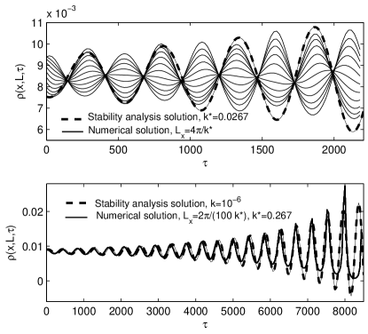
Finally, in Fig. 19 again the destabilizing state for is shown. The stability analysis predicts the most unstable wave number and its eigenvalue . The two panels show again the predicted and the simulated oscillations in a laterally wide system allowing the formation of the -mode, and in the narrow system that only has space for the -mode. Again, the agreement is convincing.
VI Conclusions and discussions
We have investigated the onset or decay of spatio-temporal patterns in a layered semiconductor-gas discharge system subject to a DC voltage. By means of linear stability analysis, we were able to derive complete phase transition diagrams, rather than only to investigate single points in parameter space in a simulation.
We have used the simplest model possible: Only the drift motion of electron and ion densities is taken into account, and the electrons are adiabatically eliminated. The semiconductor is approximated as a linear Ohmic conductor, and nonlinear effects come in only through the space charges of the ions in the gas discharge gap and through the surface charges on the gas-semiconductor interface. (We remark that particle diffusion has a smoothening effect and is not expected to generate any new structures. However, effects like gas heating or nonlinear semiconductor characteristics can create additional destabilization mechanisms.)
Methods and results of the linear stability analysis of the homogeneous stationary state and of the full numerical simulation of the initial value problem are presented. The choice of parameters is guided by the experiment described in Str2 ; they are summarized in Sect. II.5. In the experiment Str2 , the resistance of the semiconductor can be changed by a factor of 10 by photo-illumination without changing any other system parameter, and a full phase transition diagram is derived experimentally. It is seen that the system never relaxes to a spatially structured time-independent state, but depending on the resistance, it either forms a homogeneous oscillating or a spatially structured oscillating state.
Like in the experiments, the homogeneous stationary state is either stable, or it can be destabilized by a temporal (Hopf) or spatio-temporal (Turing-Hopf) mode; a purely spatial destabilization (Turing) is observed neither in experiments nor in theory. The transition from stable to unstable behavior is in about the same parameter regime in a diagram spanned by applied voltage and inverse resistance of the semiconductor . However, the parameter range where either Hopf- or Turing-Hopf-destabilization is predicted, does not agree with the experimental range where purely temporal or spatio-temporal patterns are observed. This is discussed in detail in Section IV.1.4. A possible explanation is that we might be comparing the wrong transitions. The theoretical prediction of linear perturbation theory concerns a destabilization to weak running waves of long wave lengths. These waves resemble much more the ”diffuse” moving bands reported only in the Ph.D. thesis StrTh , than the very nonlinear small dynamic filament structures described in Str2 . This suggestion actually asks for further experimental investigations. It is interesting to note that the physical mechanism of these “diffuse” bands has nothing to do with particle diffusion, but only with the Laplacian nature of the created electric fields. For further predictions on the parameter dependence of the linear instabilities, we refer to Section IV.2.
Our numerical solutions of the initial value problem in Section V agree well with our linear stability analysis within its range of validity. First of all, this proves the correct implementation of both methods. Second, for larger amplitudes, new nonlinear spatial structures appear such as the spatial period doubling in Fig. 13. For and , these oscillations actually have been seen to reach a limit cycle that corresponds to a standing wave. Of course, the full nonlinear behavior in three spatial dimensions should be investigated in the future, but the 2D results give a first indication for the behavior.
We remark finally that only the simplest possible model with nonlinear space charge effects was investigated. Of course, the model can be extended by various additional mechanisms, but obviously the simple model already contains all relevant physics to predict the onset of pattern formation in the correct parameter regime.
Acknowledgements.
The authors thank Alexander Morozov from Instituut-Lorentz, Leiden University, for advice on the numerical method described in Section III.4 and for help with its implementation. I.R. acknowledges numerous discussions with W. Hundsdorfer at the Center for Mathematics and Computer Science (CWI) Amsterdam on numerical mathematics. I.R. acknowledges financial support by ERCIM and FOM, and D.S. by FOM for their work in Amsterdam where the numerical stability analysis was performed and the numerical PDE work was initiated.Appendix A Numerical procedure
Here we describe the numerical method used for solving the initial value problem numerically. The computation is based on a finite-difference technique to solve equations (25)–(27) with boundary conditions (28)–(II.4) and periodic boundary conditions in the transversal direction.
The computational domain is a rectangular region on a two-dimensional Cartesian coordinate system , which consists of two layers – gas and semiconductor, see Figs. 1 and 20. We use a uniform vertex-centered grid in the ’vertical’ -direction with nodes
and a uniform cell-centered grid with nodes
on the ’horizontal’ x-direction. The grid is spaced such that the internal interface between semiconductor and gas region lies exactly on the grid line.
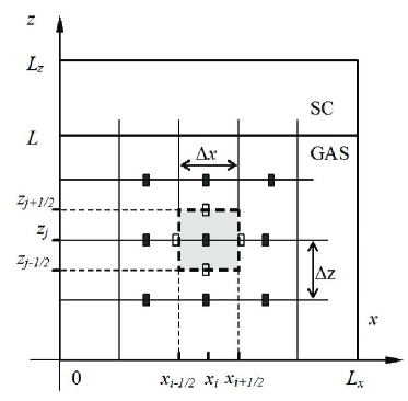
The densities and and the electric potential are evaluated on the nodes of the grid, while the and components of the electric field ( and , respectively) are calculated on the surfaces of the computational cell (Fig. 20).
To obtain a finite-difference representation of equations (25) and (26), we first integrate them over the cell volume . Let us consider in detail the equation for the ions (26). After its integration, we come to
| (101) | |||||
The subscripts and are related to (transversal) and (longitudinal) directions respectively and stands for the source term of Eq. (26).
The choice of and at the surfaces of the computational cell determines the concrete discretization method for the convective terms of Eq. (26). We used the third-order upwind-biased scheme (see, e.g., Willem , p. 83), which in - and -direction is given by
Here, the electric field components are
and is discretized as
| (103) |
For the numerical time integration, we used the extrapolated second order BDF2 method, see Willem , p. 204, Wes , p. 197, whose variable step size version has the form
| (104) |
where the superscript denotes the time with step size and step size ratio . Here contains the discretized convective terms and a source term. Note that we have dropped spatial indices in Eq. (A). Since the two-step method needs and as starting values, the explicit Euler method
| (105) |
is used for the first step . Because of the explicit time integration, we are restricted by the standard CFL stability condition.
The same space discretization technique and time integration method are used also for the electron density equation (25) that contains no temporal derivative. Note that in this case the -direction plays the role of ’time’ in (A) and (105).
To obtain a finite-difference approximation for Poisson’s equation (27), we use the traditional second order discretization:
| (108) |
This equation is valid everywhere except at the gas semiconductor interface where one has to account for a finite surface charge as well as for a discontinuity of the dielectricity constant. On this interface, the discrete version of the ’jump’ condition (30) is used instead of (108). The system of resulting difference equations is solved by a symmetrical successive over-relaxation method (SSOR), see Thomas , p. 343.
The complete numerical procedure was organized as follows. For every new th time step, first Poisson’s equation was solved using the known ion density and surface charge value in the jump condition (30), determining the electric field components in the new time step. Second, the electron density in the new time step was calculated. This determined the source term in the continuity equation for ions. Third the ion density was calculated, which finally determined the new value for the surface charge in (30).
The numerical convergence was checked by performing several calculations with different error tolerance parameters for Poisson’s equation, using refinement of the space grid, and different time stepping parameters. The number of grid nodes used in the calculations was in the and directions, respectively, for the potential in the whole gas discharge - semiconductor region, and in the and directions for the particle densities in the gas discharge region. When solving Poisson’s equation, the iteration process is stopped when the relative error is .
References
- (1) M.C. Cross and P.C. Hohenberg, Rev. Mod. Phys. 65, 851 – 1112 (1993).
- (2) U. Kogelschatz, IEEE Trans. Plasma Science 30, 1400–1408 (2002).
- (3) U. Kogelschatz, Plasma Chem. Plasma Process, 23, 1 (2003).
- (4) H. Willebrand, F.-J. Niedernostheide, E. Ammelt, R. Dohmen, and H.-G. Purwins, Phys. Lett. A 153, 437 (1991).
- (5) W. Breazeal, K.M. Flynn, and E.G. Gwinn, Phys. Rev. E 52, 1503 (1995).
- (6) C. Strümpel, Y.A. Astrov, E. Ammelt, and H.-G. Purwins, Phys. Rev. E 61, 4899 – 4905 (2000).
- (7) C. Strümpel, Y.A. Astrov, and H.-G. Purwins, Phys. Rev. E 62, 4889 – 4897 (2000).
- (8) C. Strümpel, H.-G. Purwins, and Y.A. Astrov, Phys. Rev. E 63, 026409 (2001).
- (9) C. Strümpel, Y.A. Astrov, and H.-G. Purwins, Phys. Rev. E 65, 066210 (2002).
- (10) C. Strümpel. Ph.D. thesis, Univ. Münster, Germany, 2001.
- (11) Yu.A. Astrov, E. Ammelt, S. Teperick, and H.-G. Purwins, Phys. Lett. A 211, 184 (1996).
- (12) Yu.A. Astrov, E. Ammelt, and H.-G. Purwins, Phys. Rev. Lett. 78, 3129 (1997).
- (13) Yu.A. Astrov and Y. A. Logvin, Phys. Rev. Lett. 79, 2983 (1997).
- (14) E. Ammelt, Yu.A. Astrov, and H.-G. Purwins, Phys. Rev. E 55, 6731 (1997).
- (15) Y.A. Astrov, I. Müller, E. Ammelt, and H.-G. Purwins, Phys. Rev. Lett. 80, 5341 (1998).
- (16) E.Ammelt, Yu.A. Astrov, and H.-G. Purwins, Phys. Rev. E 58, 7109 (1998).
- (17) Y.A. Astrov and H.-G. Purwins, Phys. Lett. A 283, 349 (2001).
- (18) E.L. Gurevich, A.S. Moskalenko, A.L. Zanin, and H.-G. Purwins, Phys. Lett. A 307, 299 (2003).
- (19) E.L. Gurevich, Yu.A. Astrov, and H.-G. Purwins, J. Phys. D: Appl. Phys. 38, 468 (2005).
- (20) Sh. Amiranashvili, S.V. Gurevich and H.-G. Purwins, Phys. Rev. E 71, 066404 (2005).
- (21) Y.P. Raizer, E.L. Gurevich, and M.S. Mokrov, Tech. Phys. 51, 185 (2006).
- (22) D.D. Šijačić, U. Ebert, and I. Rafatov, Phys. Rev. E 70, 056220 (2004).
- (23) D.D. Šijačić, U. Ebert, and I. Rafatov, Phys. Rev. E 71, 066402 (2005).
- (24) I. Brauer, C. Punset, H.-G. Purwins and J.-P. Boeuf, J. Appl. Phys. 85, 7569 (1999).
- (25) I. Brauer, M. Bode, E. Ammelt, H.-G. Purwins, Phys. Rev. Lett. 84, 4104 (2000).
- (26) Y.T. Zhang, D.Z. Wang and M.G. Kong, J. Appl. Phys. 98, 113308 (2005).
- (27) C. Punset, J.-P. Boeuf and L.C. Pitchford, J. Appl. Phys. 83, 1884 (1998).
- (28) L. Stollenwerk, Sh. Amiranashvili, J.-P. Boeuf and H.-G. Purwins, Phys. Rev. Lett. 96, 255001 (2006).
- (29) U. Ebert, W. van Saarloos, and C. Caroli, Phys. Rev. E 55, 1530 (1997).
- (30) D.D. Šijačić and U. Ebert, Phys. Rev. E 66, 066410 (2002).
- (31) Yu.P. Raizer, U. Ebert, and D.D. Šijačić, Phys. Rev. E 70, 017401 (2004).
- (32) A. von Engel and M.Steenbeck, Elektrische Gasentladungen (Springer, Berlin, 1934), Vol. II.
- (33) Y.P. Raizer, Gas Discharge Physics (Springer, Berlin, 2nd corrected printing, 1997).
- (34) S. Godunov, Uspekhi Mat. Nauk. 16, 243-255 (1961).
- (35) S.D. Conte, SIAM Review 8, 309-321 (1966).
- (36) E.L. Gurevich, Sh. Amiranashvili, H.-G. Purwins, J. Phys. D: Appl. Phys. 38, 1029 (2005).
- (37) W. Hundsdorfer and J.G. Verwer, Numerical solution of time-dependent advection-diffusion-reaction equations, Springer Series in Computational Mathematics 33 (Springer, Berlin, 2003).
- (38) P. Wesseling, Principles of computational fluid dynamics, Springer Series in Computational Mathematics 29 (Springer, Berlin, 2001).
- (39) J.W. Thomas, Numerical Partial Differential Equations: Conservation Laws and Elliptic Equations, Texts in Applied Mathematics 33 (Springer, Berlin, 1999).