2Institute für Theoretische Physik, Technische Universität Berlin, Hardenbergstr. 36, 10623 Berlin, Germany
3Institute for Physics of Microstructures, Russian Academy of Science, 603600 Nizhny Novgorod, Russia
Transport in semiconductor superlattices: from quantum kinetics to terahertz-photon detectors
Abstract
Semiconductor superlattices are interesting for two distinct reasons: the possibility to design their structure (band-width(s), doping, etc.) gives access to a large parameter space where different physical phenomena can be explored. Secondly, many important device applications have been proposed, and then subsequently successfully fabricated. A number of theoretical approaches has been used to describe their current-voltage characteristics, such as miniband conduction, Wannier-Stark hopping, and sequential tunneling. The choice of a transport model has often been dictated by pragmatic considerations without paying much attention to the strict domains of validity of the chosen model. In the first part of this paper we review recent efforts to map out these boundaries, using a first-principles quantum transport theory, which encompasses the standard models as special cases. In the second part, focusing in the mini-band regime, we analyze a superlattice device as an element in an electric circuit, and show that its performance as a THz-photon detector allows significant optimization, with respect to geometric and parasitic effects, and detection frequency. The key physical mechanism enhancing the responsivity is the excitation of hybrid Bloch-plasma oscillations.
1 Introduction
Ever since the pioneering work of Esaki and Tsu [ESA70], which drew attention to the rich physics and potential device applications of semiconductor superlattices, these man-made structures have remained a topic of intense research. Semiconductor superlattices have proven to be a fruitful platform for studying a wide range of transport phenomena, such as their intrinsic negative differential conductivity [SIB90], the formation of electric field domains [GRA91], Bloch oscillations [WAS93], as well as dynamical localization [HOL92] and absolute negative conductance [KEA95b] under external irradiation, just to mention a few.
These phenomena depend crucially on the relations of the energy scales involved, namely the zero-field miniband width (which is four times the interwell coupling ), the scattering rate , and the potential drop per period (, where is the applied static field and is the superlattice period). Three distinct approaches have been used to describe transport in the parameter space spanned by : miniband conduction (MBC)[ESA70, LEB70], Wannier-Stark hopping (WSH)[TSU75], and sequential tunneling (ST)[MIL94, WAC97b]. Until recently, however, the precise range of validity of these various approaches had not been addressed quantitatively. To achieve this, one much use a first-principles approach, which reduces to the standard theories in the appropriate limits. After a brief review of the standard approaches in Sect. II, we introduce in Sect. III a nonequilibrium Green function formalism, which we have used to delineate the boundaries of the different domains of validity [prl1, prl2]. We also present comparisons with Monte Carlo simulations. As we shall see, under favorable conditions it is quite possible to obtain a very accurate description with the standard methods, which is a great advantage because the first-principle Green function calculations are quite complicated and have so far successfully implemented only for rather simple scattering mechanisms (the scattering matrix elements are assumed to be independent of momentum transfer). Thus, in Sect. IV we adopt one of the standard approaches, i.e., the miniband approach, to model a superlattice THz-photon detector, taking into account the effects due to the external circuitry. We conclude that by detailed modeling substantial device performance optimization can be achieved, e.g. the detector sensivity may be improved by almost 50 % by a judicious choice of its parameters.
2 Standard transport models
Here we review the standard models used to describe transport in semiconductor superlattices. For simplicity, the results quoted in the next three subsections are written in a relaxation time approximation, but a generalization to more realistic scattering processes is possible. As an underlying Hamiltonian we use a tight-binding model:
| (1) |
Here is the overlap matrix element, is the kinetic energy perpendicular to the growth direction, and the electric field is taken into account by a shift in the site energies.
2.1 Miniband conduction (MBC)
For zero electric field Eq. (1) is diagonalized by a set of Bloch functions (here the wave function is localized in quantum well , e.g., a Wannier function) and the dispersion relation is given by the miniband . The stationary Boltzmann equation for the distribution function is then
| (2) |
where the relaxation-time is allowed to depend on energy, see, e.g., Ref.[prl1] for a suitable model. Once the solution to Eq. (2) is found, the current is calculated from
| (3) |
The electron density per period is given by
| (4) |
and is used to determine the chemical potential for a given electron density. This approach can be extended beyond the relaxation time approximation[IGN91, LEI91], but the generic features remain unchanged.
2.2 Wannier-Stark hopping (WSH)
In the presence of an electric field, the eigenstates of the Hamiltonian become the localized Wannier-Stark states,
| (5) |
with energy , and is the Bessel function of the first kind. Scattering causes hopping between the different states. Within Fermi’s golden rule, the current is given by
| (6) | |||||
Here the term arises due to the spatial overlap of the Wannier-Stark functions. The electron density per period is given by:
| (7) |
which relates to . Again, it is possible to generalize this approach to more realistic scattering mechanisms [ROT97, BRY97].
| coupling | field drop | scattering | |
|---|---|---|---|
|
Miniband conduction |
exact miniband | acceleration | golden rule |
Wannier Stark
hopping
|
exact: Wannier Stark states | golden rule | |
|
Sequential tunneling |
lowest order | energy mismatch | ”exact” spectral function |
2.3 Sequential tunneling (ST)
In this approximation the phase information is lost after each tunneling event between adjacent wells. The scattering within a well is treated self-consistently by solving for the spectral functions ; in this work we use the self-consistent Born-approximation[MAH90] for the self-energy. The transitions to neighboring wells are calculated in lowest order of the coupling yielding [WAC97, MAH90, MUR95]:
| (8) |
The carrier density is given by:
| (9) |
This approach gives quantitative agreement with experiments in weakly coupled structures when realistic models for impurity and interface scattering are employed [WAC97b, WAC97].
2.4 Summary
The important issue to recognize is that these three approaches treat scattering, external field, and coupling within different approximations. MBC does not properly include field-induced localization because of its inherent assumption of extended states, WSH treats scattering in lowest order perturbation theory (in particular, there is no broadening of the states), and ST is explicitly lowest order in the interwell coupling. The basic features of these models are summarized in Figure 1.
2.5 Nonequilibrium Green functions (NGF)
The basic building blocks are the correlation and retarded Green functions:
| (10) | |||||
| (11) |
where and and are the creation and annihilation operators for the state in well . These functions obey the Dyson and Keldysh equations, respectively, given below for the superlattice case. Ref.[HAU96] may be consulted for a text-book discussion. The observables, such as the momentum distribution, current, and electron density are computed from :
| (12) | |||||
| (13) | |||||
| (14) |
These expressions exploit the fact that in the stationary state the Green functions only depend on the time difference , and one can define a Fourier transformation via [HAU96]:
| (15) |
Without scattering between the k-states and at the Green-functions are diagonal in the well index: with the free particle Green-function . The full Green function is then determined by the Dyson equation:
| (16) | |||||
The self-energy will be written as
| (17) |
where contains contributions both from impurity and phonon scattering. The relevant expressions are
| (18) |
for impurities, while for optical phonon scattering we take (see, e.g., Ch. 4.3 of Ref. [HAU96] for the derivation):
| (19) | |||||
| (20) | |||||
It is possible to simulate acoustic phonons with a similar expression, using a small fictitious discrete energy [prl2]. In the above, we also gave the self-energy expressions needed in the Keldysh equation:
| (21) | |||||

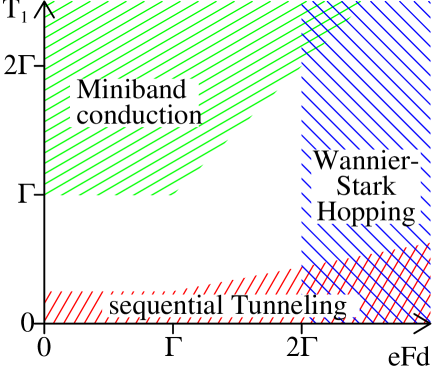
The numerical evaluation of these equations has been discussed in two recent publications [prl1, prl2], and here we just summarize our basic strategy, and give a few representative results. The first step in the analysis consists of evaluating the current-voltage characteristics for the different models, and an example of such a calculation is given in Fig. 2. We note that the Boltzmann equation gives an excellent agreement with the full quantum result, in particular for low electric fields. The additional structure in the quantum mechanical curve is a phonon-replica: the Boltzmann equation cannot capture features like this because the electric field does not enter as an energy-scale in the collision integral. It is also of interest to note that the use of a realistic electron-phonon scattering model, instead of a simple relaxation time, leads to a current-voltage characteristic which deviates significantly from the simple Esaki-Tsu shape, . By performing a large number of calculations like the one depicted in Figure 2 it is possible to develop visual criteria as to the validity of the various simplified approaches discussed in Section 2. These phenomenological considerations can be made more rigorous by examining in detail the retarded Green function, which determines the quantum mechanical correlation between quantum wells and [prl1]. For example, if the terms are of the order of , the wave-function is delocalized. By using the expressions given in Ref.[prl1], one finds that the states are delocalized if and , i.e., the Boltzmann miniband picture is a useful starting points. Similarly, by demanding that the vanish if , one can find the regime where sequential tunneling dominates. The respective ranges of validity can be presented as a “phase digram”, Fig. 3.
Additional insight to the differences between quantum kinetics and Boltzmann kinetics can be obtained by examining the momentum distribution functions. Figure 4 presents such a comparison. We direct attention to the following features. At low fields, Fig. 4(a), the distribution function can be viewed as a distorted thermal equilibrium function, and linear response theory holds, corresponding to the linear part of the current-voltage characteristics of Fig. 2 (however, at very low temperatures one should consider weak localization effects, not included in the present choice of the impurity self-energy, and the agreement between quantum and Boltzmann calculations may be weakened). If the electric field increases, electron heating becomes important. For moderate fields the distribution function resembles a distorted equilibrium function, but with an elevated electron temperature, Fig. 4(b). At even higher fields, close to the maximum in the IV-curve, the distribution function strongly deviates from any kind of equilibrium in space, Fig. 2(c). The results for quantum and semiclassical calculations look similar in the negative differential conductance (NDC) regime (not shown in Fig. 4.). The situation changes dramatically when the field energy is larger than the mini-band width, , Fig. 4(d). As the electrons can perform several Bloch oscillations in the semiclassical picture, the distribution function is almost flat withing the Brillouin zone of the miniband. The latter holds for the NGF result as well. However, the absolute values of the distribution functions differ significantly.
![[Uncaptioned image]](/html/cond-mat/9909445/assets/x6.png)
The reason is the modification in scattering processes due to the presence of the electric field, leading to significant deviations in the distribution function. We noticed this phenomenon already in our discussion of the current-voltage characteristics of Fig. 2. The strong changes in the quantum momentum distribution are further illustrated in Fig. 5.

We can summarize the results given in the first part of this paper as follows. In wide-band superlattices the Boltzmann equation gives reliable results concerning linear response at low fields, electron heating at moderate fields, and the onset of negative differential conductivity. In contrast, for high electric fields or weakly coupled SLs significant differences appear. In this case the quantum nature of transport is important and a semiclassical calculation may be seriously in error.
3 Superlattice as a THz-photon detector
3.1 Introduction
It has recently been estimated [ref35] that the room temperature current responsivity of a superlattice detector ideally coupled to the THz-photons can nearly reach the quantum efficiency in the limit of high frequencies (here is the incident radiation frequency and is a characteristic scattering frequency). This value of the responsivity is being normally considered as a quantum limit for detectors based on superconducting tunnel junctions operating at low temperatures [ref18]. For high frequencies the mechanism of the THz-photons detection in superlattices was described [ref35] as a bulk superlattice effect caused by dynamical localisation of electrons.
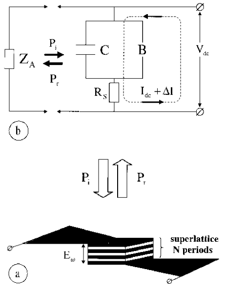
Here we describe a recent theory of the superlattice current responsivity [JAP]. We focus on relative broad-band superlattices ( meV), and field strengths smaller than the onset of negative differential conductivity. Thus, according to the analysis given above, a Boltzmann equation based description should suffice. One should note, however, that here we investigate a time-dependent situation, and that a microscopic analysis in the spirit of the first part of this paper has not, to our knowledge, been carried out. We use an equivalent circuit for the superlattice coupled to a broadband antenna (see Fig. 6), which is similar to the equivalent circuit used in resonant tunneling [ref37] and Schottky diode [ref38] simulations. The suggested equivalent circuit of the device allows one to treat microscopically the high-frequency response of the miniband electrons and, simultaneously, take into account a finite matching efficiency between the detector antenna and the superlattice in the presence of parasitic losses. Our analytic results lead to the identification of an important physical concept: the excitation of hybrid plasma-Bloch [ref39] oscillations in the region of positive differential conductance of the superlattice. Numerical computations [JAP], performed for room temperature behavior of currently available superlattice diodes, show that both the magnitudes and the roll-off frequencies of the responsivity are strongly influenced by this effect. The excitation of the plasma-Bloch oscillations gives rise to a resonant-like dependence of the responsivity on the incident radiation frequency, improving essentially the coupling of the superlattice to the detector antenna. We will also show that peak current densities in the device and its geometrical dimensions should be properly optimized in order to get maximum responsivity for each frequency of the incident photons. Finally, we will present numerical estimates of the responsivity for the 1-4 THz frequency band and compare its value with the quantum efficiency of an ideal detector.
3.2 Theoretical formalism
The exact solution of the time-dependent Boltzmann equation in the relaxation time approximation for an arbitrary time-dependent electric field can be presented in the form of a path integral [ref41]:
| (22) |
Using Eqs.(3) and (22) we find the time-dependent current describing ac transport in a superlattice, with electron performing ballistic motion in a mini-band according to the acceleration theorem and suffering scattering [ref2, ref3]:
| (23) |
where is the voltage across the superlattice perpendicular to the layers, is the superlattice length, is the number of periods in the superlattice sample, , is the area of the superlattice, is the superlattice mesa radius, and
| (24) |
is the characteristic current density. The integration over in Eq.(24) must be carried out over the Brillouin zone .
The peak current density and the scattering frequency can be considered as the main parameters of the employed model. They can readily be estimated from experimentally measured or numerically simulated values of and . For both degenerate and non-degenerate electron gas one gets [ref2, ref3]
| (25) |
if , where is the equilibrium thermal excitation energy, is the Fermi energy of degenerate electrons, is the density of states effective mass near the miniband bottom, and is the effective mass of electrons along the superlattice axis. In the particular case of the Boltzmann equilibrium distribution function Eq.(24) yields [ref3] , where are the modified Bessel functions.
We now suppose that in addition to the dc voltage , an alternating sinusoidal voltage with a complex amplitude is applied to the superlattice:
| (26) |
Generally, can be found from an analysis of the equivalent circuit given in Fig. 6. We write the ac voltage amplitude as ; both and can be obtained self-consistently taking account of reflection of the THz photons from the superlattice and their absorption in the series resistor .
Making use Eq.(23) we obtain [ref3]:
| (27) |
where
| (28) |
According to Eq.(27), electrons in a superlattice miniband perform damped Bloch oscillations with the frequency , and the phase modulated by the external ac voltage.
Equation (27) contains, as special cases the following results: (i) a harmonic voltage () leads to dynamical localisation, and current harmonics generation with oscillating power dependence [ref3]; (ii) a dc current- voltage characteristics of the irradiated superlattice shows resonance features (‘Shapiro steps’) leading to absolute negative conductance [ref3, ref5, ref7, ref17]; (iii) and to generation of dc voltages (per one superlattice period) that are multiples of [ref13].
3.3 Current responsivity
We define the current responsivity[ref18] of the superlattice detector as the current change induced in the external dc circuit per incoming ac signal power :
| (29) |
This definition takes into account both the parasitic losses in the detector and the finite efficiency for impedance-matching of the incoming signal into the superlattice diode.
It can be shown [JAP], that in the small-signal approximation both the dc current change and the power absorbed in the superlattice are proportional to the square modulus of the complex voltage . This circumstance permits us to calculate self-consistently for given values of the incoming power, making use a linear ac equivalent circuit analysis and, then, find the current responsivity .
The results of the calculation of the superlattice current responsivity are presented in the following form:
| (30) |
where
| (31) |
is the superlattice current responsivity under conditions of a perfect matching and neglecting parasitic losses, . [ref35]
The factor in Eq. (30) describes the effect of the electrodynamical mismatch between the antenna and the superlattice and the signal absorption in the series resistance
| (32) |
The first factor in Eq. (32) describes the reflection of the THz-photons due to mismatch of the antenna impedance and the total impedance of the device , with the second one being responsible for sharing of the absorbed power between the active part of the device described by the impedance and the series resistance .
The superlattice impedance is defined as
| (33) |
where is the superlattice conductance, is the capacitance of the superlattice, and is the average dielectric lattice constant.
Finally, the last factor in the denominator of Eq. (30) describes the redistribution of the external bias voltage between the dc differential resistance of the superlattice and the series resistance , with the dc voltage drop on the superlattice being determined by the solution of the well-known load equation [ref18]
| (34) |
3.4 Superlattice dielectric function. Hybridisation of Bloch and plasma oscillations
We next analyze the condition of optimized matching of the superlattice to the incident radiation. Assuming the limit of negligible series resistance this condition can be obtained from the solution of the equation
| (35) |
for the complex frequency . This solution determines the resonant line position and the line width at which the absorption in the superlattice tends to its maximum value.
One can transform Eq. (35) to the following form:
| (36) |
where
| (37) |
is the dielectric function of the superlattice, with the dc field being applied to the device [ref38], and is defined by
| (38) |
In the high-frequency limit the solution of Eq. (35) coincides with the solution of the equation
| (39) |
describing the eigenfrequencies of the hybrid plasma-Bloch oscillations in a superlattice, [ref38]
| (40) |
where is the plasma frequency of electrons in a superlattice. The plasma frequency can be given in terms of the small-field dc conductivity or, equivalently, in terms of the peak current density
| (41) |
Equation (41) reduces in the particular case of wide-miniband superlattices () to the standard formula .
In the limiting case of small applied dc electric fields one finds from Eq. (40) the plasma frequency , while in the opposite case , the Bloch frequency is recovered. The scattering frequency in Eq. (40) is responsible for the line width of the plasma-Bloch resonance.
We have calculated the hybrid plasma-Bloch oscillation frequency , using Eqs. (40) and (41), for the typical values of the superlattice parameters , Å, kV/cm, THz for different values of the current densities (see Fig. 7). For small values of the current densities kA/cm2 the frequency of the hybrid oscillation increases with applied voltage in all range of the parameter . On the other hand, for higher values of the current densities kA/cm2 the hybrid oscillation’s frequency starts to decrease with increasing bias voltage in the sub-threshold voltage range . Then, at super-threshold voltages , starts to increase again tending to the Bloch frequency. It is important to note that at high values of the dc current densities the hybrid plasma-Bloch oscillations become well defined eigenmodes of the system (). Therefore, an essential improvement of the matching efficiency between antenna and the superlattice can be expected in the high- frequency range due to a resonant excitation of this eigenmode in the device.
3.5 High-frequency limit
Let us compare the high-frequency limit of the responsivity of the superlattice with the quantum efficiency which is believed to be a fundamental restriction for the responsivity of superconductor tunnel junctions[ref18]. This quantum efficiency (or quantum limit) corresponds to the tunnelling of one electron across the junction for each signal photon absorbed[ref18], with a positive sign of the responsivity.
In our case the mechanism of the photon detection is different (see Fig. 8). Electrons move against the applied dc electric force due to absorption of photons. At the responsivity is negative, indicating that one electron is subtracted from the dc current flowing through the superlattice when the energy is absorbed from the external ac field. One half of this energy is needed for the electron to overcome the potential barrier which is formed by the dc force, with another half being delivered to the lattice due to energy dissipation. If the applied dc voltage is strong enough, i.e. , dissipation plays no essential role in the superlattice responsivity. In this case the energy should be absorbed from the ac field in order to subtract one electron from the dc current simply due to the energy conservation law.
3.6 Excitation of the plasma-Bloch oscillations
For demonstration of the frequency dependence of the superlattice current responsivity in the THz-frequency band we will focus on the GaAs/Ga0.5Al0.5As superlattices specially designed to operate as millimeter wave oscillators at room temperature. In Ref. [ref43] wide-miniband superlattice samples with Å, meV, , were investigated experimentally. They demonstrated a well-pronounced Esaki- Tsu negative differential conductance for kV/cm with the high peak current of the order of kA/cm2. The measured value of the peak current is in a good agreement with the estimate kA/cm2 for , 300 K based on Eq. (24), if one assumes an equilibrium Boltzmann distribution for the charge carriers. From the peak electric field and current we find the scattering and plasma frequencies THz, THz, respectively, assuming for the average dielectric lattice constant. The maximum frequency for the semiclassical approach to be valid for these samples is THz.
Figure 9 shows the frequency dependence of the normalised current responsivity calculated for three values of the peak current density in the superlattice, i.e. 13, 130, and 300 kA/cm2 and for three values of the peak electric field, 4, 9, and 13 kV/cm. We also use the typical values for the superlattice length m (superlattice consists of 100 periods), and assume m for the superlattice mesa radius [ref43, ref44, ref45]. We choose for the series resistance of the device in the THz- frequency band, i.e. the same value as for resonant tunnelling diodes having the same radius of mesas [ref37]. The calculations are performed in the region of the positive differential conductance for dc bias voltage close to the peak voltage ( )
For kV/cm ( THz) Fig. 9 demonstrates well-pronounced resonant behavior of the normalised responsivity as a function of frequency. The resonance frequency and the maximum value of the responsivity rise if the peak current density increases. For kA/cm2 the normalised responsivity reaches its maximum value ( A/W) at frequency THz. For higher values of the peak electric fields kV/cm ( THz) and kV/cm ( THz) the resonance line-widths are broadened due to implicit increase of the scattering frequencies. In particular, for kV/cm, kA/cm2 the normalised responsivity has an almost constant value ( A/W) up to THz and, then, rapidly decreases. The frequency behavior of the normalised responsivity originates from excitation of the plasma- Bloch oscillations in the superlattice. We indicate in Fig. 9 the positions of the hybrid frequencies with arrows. For small peak electric fields (low values of the scattering frequencies) the hybrid frequency corresponds to the maximum of the normalised responsivity. For higher values of the peak field (higher values of the scattering frequencies) it corresponds to the roll-off frequency at which the responsivity starts to decline.
3.7 Optimized superlattice length
The enhancement of the normalised responsivity requires an optimum matching efficiency of the superlattice to the broad-band antenna and minimization of the parasitic losses in the series resistor. These requirements impose an optimum length of the superlattice for each chosen frequency of the incoming THz-photons and series resistance.
We show in Fig. 10 the dependence of the normalised responsivity on the number of the superlattice periods for THz.We used for calculation m, kA/cm2, , and three values of the series resistance , 30 and 50 . For all three values of the series resistance the responsivity displays a well pronounced maximum for the optimum number of the superlattice periods . The value of increases with increasing of the series resistance ( for = 10 , for = 30 and for for = 50 ). This result can be readily understood by recalling that a larger volume of the superlattice minimizes parasitic losses for higher values of the series resistance because of reduction of the sample’s capacitance.
In addition to the examples discussed here, Ref. [JAP] reports several other aspects of the superlattice responsivity, such as bias voltage dependence, optimized peak current density etc.
3.8 Conclusions
We have illustrated here the steps required to perform a superlattice device optimization. These include: (i) Consideration of the frequency dependence of the superlattice. Here a truly microscopic analysis is not yet available, but a Boltzmann equation based theory should be applicable, with due caution. (ii) The impedance matching between the antenna and the superlattice must be optimized. (iii) The effect of parasitic losses must be included in the analysis. One of the main results emerging from our analysis is the importance of collective excitations: the hybridized plasma-Bloch oscillations both enhance the responsivity and increase the roll-off frequency. It is found that an optimized superlattice can have a responsivity which approaches 10 % of an ideal superconducting tunnel junction. The great advantage, of course, is that superlattice based detectors work even at room temperature, and this property should offer a wide range of applications.
References
- [1] ESA70[1] L. Esaki and R. Tsu, IBM J. Res. Develop. 14, 61 (1970).
- [2] SIB90[2] A. Sibille, J. F. Palmier, H. Wang, and F. Mollot, Phys. Rev. Lett. 64, 52 (1990).
- [3] GRA91[3] H. T. Grahn, R. J. Haug, W. Müller, and K. Ploog, Phys. Rev. Lett. 67, 1618 (1991).
- [4] WAS93[4] C. Waschke et al., Phys. Rev. Lett. 70, 3319 (1993).
- [5] HOL92[5] M. Holthaus, Phys. Rev. Lett. 69, 351 (1992).
- [6] KEA95b[6] B. J. Keay et al., Phys. Rev. Lett. 75, 4102 (1995).
- [7] LEB70[7] P. A. Lebwohl and R. Tsu, J. Appl. Phys. 41, 2664 (1970).
- [8] TSU75[8] R. Tsu and G. Döhler, Phys. Rev. B 12, 680 (1975).
- [9] MIL94[9] D. Miller and B. Laikhtman, Phys. Rev. B 50, 18426 (1994).
- [10] WAC97b[10] A. Wacker and A. P. Jauho, Physica Scripta T69, 321 (1997).
- [11] Aguado[11] R. Aguado, G. Platero, M. Moscoso, and L. L. Bonilla, Phys. Rev. B 55, 16053 (1997)
- [12] prl1[12] A. Wacker and A. P. Jauho, Phys. Rev. Lett. 80, 369 (1998).
- [13] prl2[13] A. Wacker, A. P. Jauho, S. Rott. A. Markus, P. Binder, and G. H. Döhler, Phys. Rev. Lett. 83, 836 (1999).
- [14] IGN91[14] A. A. Ignatov, E. P. Dodin, and V. I. Shashkin, Mod. Phys. Lett. B 5, 1087 (1991).
- [15] LEI91[15] X. L. Lei, N. J. M. Horing, and H. L. Cui, Phys. Rev. Lett. 66, 3277 (1991).
- [16] ROT97[16] S. Rott, N. Linder, and G. H. Döhler, Superlattices and Microstructures 21, 569 (1997).
- [17] BRY97[17] V. V. Bryksin and P. Kleinert, J. Phys.: Cond. Mat. 9, 7403 (1997); S. Rott et al., Physica E (Amsterdam) 2, 511 (1998).
- [18] MAH90[18] G. D. Mahan, Many-Particle Physics (Plenum, New York, 1990).
- [19] MUR95[19] S. Q. Murphy, J. P. Eisenstein, L. N. Pfeiffer, and K. W. West, Phys. Rev. B 52, 14825 (1995).
- [20] WAC97[20] A. Wacker, in Theory of transport properties of semiconductor nanostructures, edited by E. Schöll (Chapman and Hall, London, 1998), Chap. 10.
- [21] HAU96[21] H. Haug and A.-P. Jauho, Quantum Kinetics in Transport and Optics of Semiconductors (Springer, Berlin, 1996).
- [22] ref35[22] A. A. Ignatov, E. Schomburg, J. Grenzer, S. Winnerl, K. F. Renk and E. P. Dodin, Superlattices & Microstructures 22, 15 (1997).
- [23] ref18[23] For a review, see J. R. Tucker and M. J. Feldman, Rev. Mod. Phys. 57, 1055 (1985).
- [24] JAP[24] A. A. Ignatov and A. P. Jauho, J. Appl. Phys. 85, 3643 (1999)
- [25] ref37[25] T. C. L. G. Sollner, W. D. Goodhue, P. E. Tannenwald, C. D. Parker, and D. D. Peck, Appl. Phys. Lett. 43, 588 (1983).
- [26] ref38[26] H. C. Torrey and C. A. Whitmer, Crystal Rectifiers (McGraw-Hill, New York, 1948), p. 336.
- [27] ref39[27] A. A. Ignatov and V. I. Shashkin, Sov. Phys. JETP. 66, 526 (1987).
- [28] ref41[28] R. G. Chambers, Proc. Phys. Soc. (London) A 65, 458 (1952).
- [29] ref2[29] R. Tsu and L. Esaki, Appl. Phys. Lett. 19, 246 (1971).
- [30] ref3[30] A. A. Ignatov and Yu. A. Romanov, Sov. Phys. Solid State 17, 2216 (1975); Phys. Status Solidi B 73, 327 (1976).
- [31] ref5[31] A. A. Ignatov and Yu. A. Romanov, Radiophysics and Quantum Electronics (Consultants Bureau, N.Y., 1978) Vol. 21, p. 90.
- [32] ref7[32] M. Holthaus, Phys. Rev. Lett. 69, 351 (1992).
- [33] ref17[33] A. A. Ignatov, K. F. Renk, and E. P. Dodin, Phys. Rev. Lett. 70, 1996 (1993); J. B. Xia, Phys. Rev. B 58, 3565 (1998).
- [34] ref13[34] A. A. Ignatov, E. Schomburg, J. Grenzer, K. F. Renk, and E. P. Dodin, Z. Phys. B 98, 187 (1995).
- [35] ref43[35] E. Dutisseuil, A. Sibille, J. F. Palmier, F. Aristone, F. Mollot, and V. Thietty-Mieg, Phys. Rev. B 49, 5093 (1994).
- [36] ref44[36] E. Schomburg, A. A. Ignatov, J. Grenser, K. F. Renk, D. G. Pavel’ev, Yu. Koschurinov, B. Ja. Melzer, S. Ivanov, S. Schaposchnikov, and P. S. Kop’ev, Appl. Phys. Lett. 68, 1096 (1996).
- [37] ref45[37] S. Winnerl, E. Schomburg, J. Grenser, H.-J. Regl, A. A. Ignatov, A. D. Semenov, K. F. Renk, D G. Pavel’ev, Yu. Koschurinov, B. Ja. Melzer, V. Ustinov, S. Ivanov, S. Schaposchnikov, and P. S. Kop’ev, Phys. Rev. B 56, 10 303 (1997).