Interband Light Absorption at a Rough Interface
Abstract
Light absorption at the boundary of indirect-band-gap and direct-forbidden gap semiconductors is analyzed. It is found that the possibility of the electron momentum nonconservation at the interface leads to essential enhancement of absorption in porous and microcrystalline semiconductors. The effect is more pronounced at a rough boundary due to enlargement of the share of the interface atoms.
pacs:
78.66.-w, 78.55.MbI Introduction
It is well known that the direct interband electron transitions is the main mechanism of light absorption in pure semiconductors. These transitions are direct owing to the momentum conservation low for the excited electron. The momentum, which this electron obtains from the light wave (, where is the wavelength of the light), is small in comparison with the electron momentum in the crystal (, where is the electron wavelength). It is clear, however, that the momentum is not conserved if the absorption takes place at the crystal boundary or at the interface between two crystals. The possibility of indirect electron transitions at the interface results in enhancement of the absorption. This means that the considerable enhancement of light absorption has to be expected in porous and microcrystalline semiconductors where the share of the interface atoms is sufficiently large.
This interface mechanism of light absorption becomes most important if indirect electron transitions are more preferable than the direct ones. This happens, first, in indirect-band-gap semiconductors where the electron transition to the side valley in the bulk should be accompanied by the electron-phonon or electron-impurity interaction. Second, this happens in direct-forbidden-band-gap semiconductors where the direct electron transitions between the top of the valence band and the bottom of the conduction band are prohibited.
Both possibilities are considered in this paper. We investigate the frequency dependence of the absorption at the fundamental absorption edge and estimate the relative value of the interface absorption. We consider also the interband light absorption at a rough interface. Such interface is characteristic for the intercrystallite boundary in porous and microcrystalline semiconductors.
II The model
We consider the light absorption at the surface of the semiconductor quantum dot or the crystallite embedded in an insulator media. Suppose that each size of the crystallite much exceeds the lattice constant. On this assumption the envelope function approximation is valid. Moreover, this assumption allows us to consider the light absorption as inelastic scattering of the electron at the interface if the electron wavelength is sufficiently small. We introduce the Cartesian coordinate system, where the axis is normal to the interface and assume that semiconductor occupies the region .
The probability for the photon to be absorbed in the crystallite is
| (1) |
where and are the fundamental constants, is the photon frequency, is the refraction index, is the area of the crystallite side where the absorption is considered, and are the electron momenta, and are their components, and are the energies of the electron in the conduction and valence bands. The electric field of the light is directed along the axis; and are the wave functions of the electron before the excitation (in the valence band) and after it (in the conduction band) correspondingly. Wave functions and are determined by the band structure of the crystallite and the boundary conditions for the envelope wave functions at the interface between the crystallite and the insulator.
To consider the Coulomb interaction, which occurs between the exited electron and the hole in the valence band, we have to input the weight factor [where , and is the effective Bohr radius] into the sum (1) [1]. The Coulomb interaction becomes important if the electron and the hole are too close to the band extrema, so that their wavelengths are large. In this case the electron density at the place where the hole is situated is not small.
It is possible to change summation in Eq. (1) by integration over the electron energy and parallel-to-interface components of the momentum . We obtain
| (2) | |||
| (3) | |||
| (4) |
and are the effective masses of the electron in the conduction and valence bands respectively, and are the numbers of atoms in the crystallite and at the interface, and is the gap. The limits of integration are determined by the region where the expressions under the square roots in the integrand are positive.
III Boundary conditions for the envelope wave function
Boundary condition at the plane interface
Interface of semiconductors with nondegenerate band structure
Let be the interface between semiconductor () and an insulator (). For a simple nondegenerate electron spectrum the boundary conditions for the envelope wave function at the plane interface can be written in the form [2]:
| (5) | |||
| (6) |
Where and are the parameters of the boundary conditions, which relate the envelopes at the different sites at the interface. It is important that these sites are close to the interface. The generally accepted form of the boundary conditions [3] can be obtained from Eq. (5) if we expand at the interface assuming where . Then we find
| (10) |
The values of , , and are independent of the electron energy and can be used as the fenomenological parameters. The determinant of the matrix should be equal to (where and are effective masses of the electron on each side of the interface) in order to ensure the conservation of the electron probability flux at the interface.
It follows from Eq. (10) that, in general, , , , and . To understand the physical meaning of this estimation, let us consider the electron scattering at the interface. The envelope wave function of the electron is
Where is the momentum of the electron, and () is the decay exponent of the electron wave function in the insulator. We can use the boundary conditions (10) to obtain the reflection coefficient
| (11) |
The pole of this expression determines the energy of the electron level, which separates from the band at the interface. We can rewrite Eq. (11) as follows:
| (12) |
where is the decay exponent of the electron wave function of the interface state. Eq. (12) allows to relate the value of with the energy of the interface level. We see that the parameter indicates the value of separation of the interface level apart off the band extremum. Indeed, for , i.e., the separation is of the order of the band width. However, the interface level becomes close to the band extremum when .
Interface of semiconductors with degenerate band structure
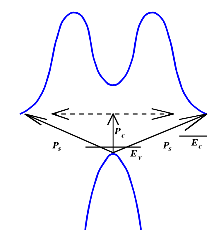
The boundary conditions for the envelope wave function becomes more complicated if the intervalley or interband degeneracy occurs in the band structure of the semiconductor. For simplicity, let us consider the two-valley conduction band presented on Fig. 1. The boundary conditions for the electron in this band can be written as follows [2]:
| (13) | |||
| (14) | |||
| (15) |
Where parameters and are independent of the electron energy. The probability flux conservation holds at the interface for arbitrary electron energies. To ensure this, the parameters of the boundary conditions (13) must satisfy the following relations:
| (16) | |||||
| (17) | |||||
| (18) |
Where and are the effective masses of the electron in the central and side valleys of the conduction band of the semiconductor, and is the effective mass in the insulator.
An important simplification aries then the large band offset occurs at the contact of a two-valley semiconductor and an insulator. If so, then , where the value can be considered as independent of the electron energy. Eliminating from Eqs. (13), we find
| (19) | |||
| (20) |
where and are known functions of , , and . The boundary conditions (19) looks quite alike Eq. (5). Therefore, Eq. (10) holds in this case too. This allows us to use Eqs. (5, 10) to consider the light absorption also at the interface of indirect-band-gap semiconductor.
Boundary conditions at a rough interface
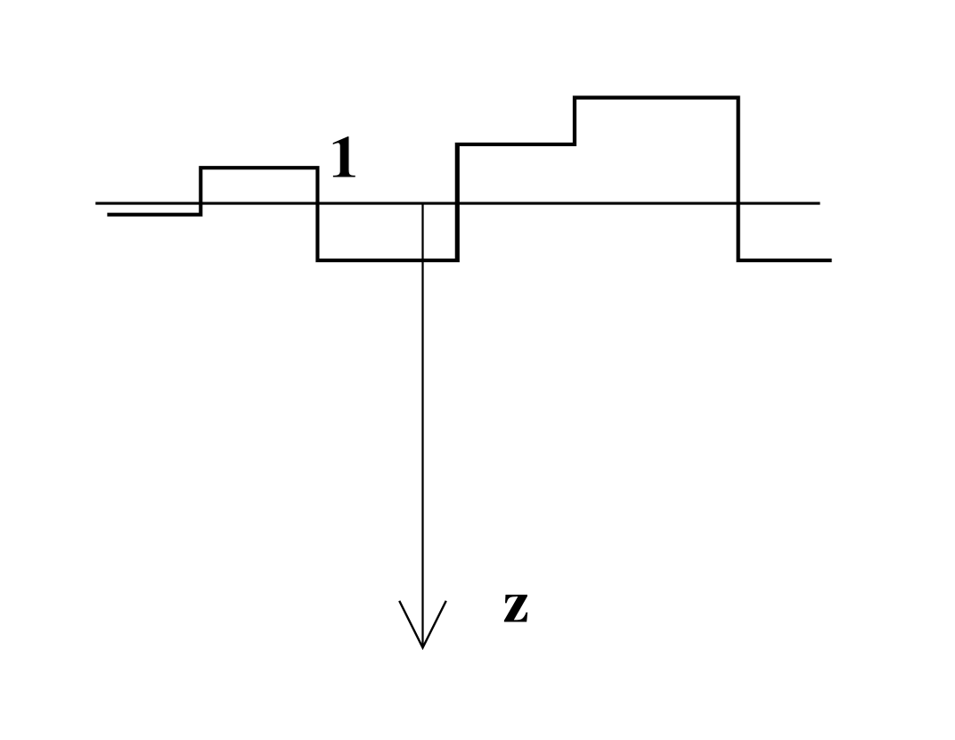
Nonlocal form of the boundary conditions (5) can be used to obtain the boundary conditions for the envelope wave function at a rough interface. We consider the special form of a rough interface that is presented on Fig. 2. The interface looks like an array of the plane areas of the same crystallographic orientation. The random function of the coordinates in plane determines the positions of these areas relative to .
We assume the average height of roughnesses to be small in comparison with the electron wavelength. Then it is possible to describe the rough interface by means of the correlation function . For the homogeneous rough interface , i.e., the correlation function is the function of one variable: . There are two parameters that are most important when the statistical properties of a rough interface is considered: and the correlation length — the mean attenuation length of the correlation function. In our model the correlation length can be associated with the mean size of the plane area (Fig. 2). We shall analyze the relation between the light absorption and the parameters and .
The special form of the rough interface (Fig. 2) allows us to apply the boundary conditions (5), which are applicable at a plane interface, at each plane . Note that these boundary conditions are not applicable at the vicinity of the corner points (like point 1 on Fig. 2). We assume the mean size of the plane areas to be large in comparison with the lattice constant, so that the relative number of the corner points is small.
To obtain the boundary conditions at the rough interface, it is necessary to expand the envelopes in Eq. (5) at , instead of . This means that values in Eq. (10) should be replaced by , so that the matrix of the boundary conditions becomes of the form
| (21) |
where are the components of the boundary conditions matrix (10) at the plane interface.
It is important that now the boundary conditions matrix depends on . This results in the diffuse components of the wave functions. We write the envelopes as the sum of their average and diffuse components [5]
| (22) |
To obtain the boundary conditions for and , we substitute the envelopes (22) into Eq. (10) using the boundary conditions matrix (21). We also have to average these equations and subtract the average equations from the initial ones. Then we obtain
| (23) | |||
| (24) | |||
| (25) | |||
| (26) |
The values , , and are omitted; they are small if .
We use Eqs. (23) to consider the electron scattering at the rough interface. The envelope wave function can be written in the form:
| (27) | |||
| (28) | |||
| (29) | |||
| (30) | |||
| (31) |
where is the electron energy. It follows from Eq. (27) that . We use last two equations (23) to express the diffuse components and as functions of , , and . The reflection () and transmission () coefficients can be obtained then from first two equations (23). These equations accept the form of Eq. (10) if we introduce the effective parameters of the boundary conditions as follows:
| (32) | |||
| (33) | |||
| (34) | |||
| (35) |
Where is the correlation function of the rough interface, and is its Fourier transform
For the diffuse component we obtain
| (36) | |||
| (37) |
We should emphasize two-fold influence of the interface roughness. First, the roughness of the interface results in the diffuse component of the scattered wave. This component is always small for the long wavelength electrons and vanish when . Second, the effective parameters of the boundary conditions depend on the interface roughness. This effect depends on the relation between the electron wavelength and the correlate length of the rough interface. Indeed, we can assume if . Then the corrections to the effective parameters of the boundary conditions (32), coursed by the roughnesses, become proportional to and vanish when .
Corrections to become independent of when . This is clear from Eq. (32) because in this case . It is easy to understand the reason. Formally, the roughnesses, each size of which is less then the electron wavelength, could be taken into account when the parameters and of the boundary conditions are obtained. In that consideration the roughnesses affect the value of these parameters but don’t make them dependent on [2]. It follows from Eq. (32) that dependent corrections to are of the order of ; this is in agreement with estimations [2].
It should be noted that values of are not real at a rough interface. The reason has to do with the diffuse component of the scattered wave that spoils the time-inversion symmetry.
IV Interband light absorption at a plane interface
Interface light absorption in direct-forbidden gap semiconductors
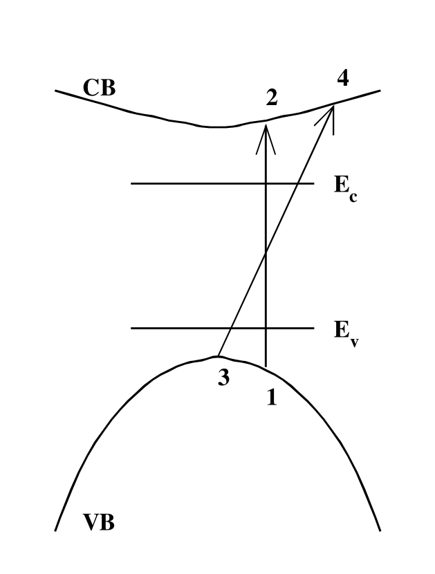
Let us consider the light absorption at the interface between semiconductor () and an insulator (). The band structure of the semiconductor is presented on Fig. 3. We can write the electron wave functions as follows:
| (40) | |||
| (41) | |||
| (44) |
Where and are the Bloch amplitudes in the conduction and valence band respectively; are decay exponents of the wave functions apart off the interface; , , , and are the reflection and transmission coefficients. It is possible to relate these values with positions of the interface levels (see Eq. (12))
| (45) |
where , and .
In direct-forbidden gap semiconductors . We assume , where is the periodic function of that is not vanished at . Then for the interband matrix element we obtain
| (46) | |||
| (47) | |||
| (48) |
We see that energy dependence of is sensitive to the position of the interface levels and , whether or not they are close to the corresponding band extrema. If we assume the Coulomb exponent as independent of q, then the result of integration (2) can be written as follows:
| (49) | |||
| (53) |
Interface light absorption in indirect-band-gap semiconductors
The band structure of the semiconductor is presented on Fig. 1. For simplicity, we assume the nondegenerate valence band. There are two valleys in the conduction band: the central valley with the minimum at the center of Brillouin zone, and the side valley at the edge of it. It is important that the side valley of the conduction band is situated in the direction of the normal to the interface.
We write the electron wave functions as follows:
| (54) | |||
| (55) |
Where , , and are the Bloch amplitudes in the valence band, the central and side valleys of the conduction band; , , and are components of the wave numbers in these valleys. The coefficients , and are determined by the boundary conditions for the envelopes.
For the interband matrix element we find [2]
| (56) | |||
| (57) |
and are the electron energies in the conduction and valence bands respectively, is the coefficient depended on the interface structure, and is the unit cell.
The energy dependence of (for ) is the same as Eq. (46), therefore
| (58) |
where is determined by Eq. (49), and is the dimensionless parameter, which has been aroused from the first term of the expression (56). Two terms in the square brackets of Eq. (58) can be interpreted as follows: the first one corresponds to the immediate transition of the electron to the side valley at the interface, second term corresponds to the excitation of the electron to the virtual interface state of the central valley subsequented by conversion to the side valley, it prevails if the valleys minima are close ().
The Coulomb interaction between the electron in the conduction band and hole in the valence bands can affect the frequency dependence of the absorption. Indeed, is independent of only if . Otherwise, if , it is proportional to ; in this case the exponent changes, so that when (where , ).
Thus, the frequency dependence of the absorption at the fundamental absorption edge essentially depends on the conditions at the interface. Namely, whether or not the interface electron levels are close to the corresponding bands extrema.
V Light absorption at a rough interface
According to Eq. (22), we write
| (59) |
where and are the average and diffuse components of the corresponding wave functions:
| (61) |
where and are the coefficients (36) for the valence and conduction bands respectively. By substituting the wave functions (61) into Eq. (40), we express the matrix element as follows:
| (63) | |||
| (64) | |||
| (65) | |||
| (66) |
We have to obtain the square module of Eq. (63) and then to average it over the realizations of the random function . For we have
The expressions (V) allow to estimate influence of the roughness on the value and the frequency dependence of the absorption. Note that the value is of the same form as that for the plane interface. The main difference concerns parameters of the boundary conditions Eq. (32), wherein an influence of the interface roughness has been taken into account. This results in the shift of the interface levels that manifests itself in the frequency dependence of the absorption. This effect is most important if the interface electron levels are close to both, valence and conduction, bands or if the interface is smooth; the values of and are not small in these cases.
Indeed, the expressions (69) and (71) determine an influence of the diffuse components of the scattered waves on the absorption; the values of these components are as small as . On the contrary, this small parameter is absent in Eq. (68) that determines an influence of the average component (i.e., position of the interface electron level) on the absorption. However, Eq. (68) is proportional to . This value is small if the interface level is not close to any band. Then the values of (69) and (71) may be of the same order or even exceed (68).
Comparing (69) and (71) with (68), we find that the roughness influence on the absorption is determined by the value
| (72) | |||
| (73) |
The correlation length of the rough interface is also important for the light absorption. We can assume if . It can be shown that in this case. It is easy to understand the reason. Roughnesses, the mean length of which (Fig. 2) essentially exceeds the electron wavelength, couldn’t affect the electron properties of the interface.
In the opposite limiting case the roughness influence is determined by the term . Enhancement of the absorption in this case arises due to an increase of the number of the interface atoms , in vicinity of which the interband absorption with the momentum nonconservation occurs.
The interesting situation arises when . In this case the diffuse scattering that is described by the term leads to the change in the frequency dependence of the absorption. This means the rapid increase of absorption at the high frequencies when , so that the exponent changes its value from .
We considered the interband light absorption at the interface and found that possibility of the electron momentum nonconservation leads to enhancement of the absorption in the small microcrystallite. To estimate the value of the interface absorption, we have to compare the absorption of the microcrystalline solid composed from the crystallites under consideration, , with the light absorption in the bulk semiconductor. Here is length of the crystallite under consideration, is the main size of the region at the interface where the interband electron transitions with the momentum nonconservation are possible. To estimate this value, we can use Eqs. (45, 46): if the interface electron levels are close to both (conduction and valence) bands extrema, if the interface level is close to any (conduction or valence) band extremum, and if both interface levels separate too far off the band extrema. The small value characterizes the ratio of the number of atoms at this interface region to the number of atoms in the whole of solid.
In order to the interface absorption becomes important in Ge and the indirect-band-gap semiconductors of the AIIIBV group this small value should exceed the small parameter of electron-phonon interaction (this value is about 10-3–10-2). In these semiconductors the interface absorption essentially increases due to the intervalley conversion, which is determined by the second term in Eq. (58). That is possible if .
The main mechanism of light absorption in bulk Si is the impurity absorption. In order to the interface absorption becomes significant in this material, the number of the interface atoms should exceed the number of impurities. It seems possible that considered here indirect interband electron transitions at the interface are responsible for an increase of luminescence of the porous Si (see [7] and references therein).
Enhancement of the light absorption at the fundamental absorption edge has to be expected in direct-forbidden gap semiconductors, wherein the direct electron transitions between the band extrema are prohibited. The essential difference in the effective masses of the valence and conduction bands is favourable for the effect. Such situation is characteristic for transition metal oxides semiconductors [9]. The conduction band in these materials composed mainly of orbitals of the metal. These orbitals are strongly localized. For this reason the conduction band is narrow and become even flat in certain direction (- for TiO2). It is important that direct interband electron transition is dipole-forbidden in this material. There is two-fold advantage from the indirect electron transitions. First, they are allowed, i.e., the dipole matrix element of the indirect transitions is not small. Second advantage arises due to the large density of states for the electron in the conduction band.
Let us compare the interband transitions in the bulk of semiconductor and at the interface (Fig. 3). The absorption is proportional to the density of electron states in each band. The density of states in the conduction band of TiO2 essentially exceeds that in the valence band. Nevertheless, it is the density of electron states in the valence band which determines the absorption in the bulk of crystal. This happens because of the momentum conservation law, which makes the electron states with the large momentums inaccessible for the exited electrons. On the contrary, indirect electron transitions make such states accessible.
We can use Eq. (49) to estimate the value of absorption coefficient of the microcrystalline direct-forbidden gap semiconductor:
where is the absorption coefficient of the bulk monocrystal, is width of the valence band (meV and eV for TiO2 [9]). Thus, the interface mechanism of the absorption becomes comparable with the bulk one for the microcrystalline TiO2 the mean size of the crystallite in which is nm. Significant increase of optical absorption has been observed in the microcrystalline BaTiO3 [10].
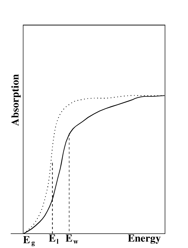
We found that the absorption value and its frequency dependence at the fundamental absorption edge are sensitive to the structure of the interface. Thus, essential increase of the absorption has to be expected at a smooth interface. For such interface the main size of the interface region (i.e., the region at the interface where one crystal structure changes into another) much exceeds the lattice constant. It is found that at a smooth interface [6], so that , and the interband matrix element increases, because it no longer proportional to the small ratio [see Eqs. (45, 46)]. Indeed, the significant (in 100 times) enhancement of the light absorption has been observed at the interface a-Si/mc-Si [8].
The possible existence of the interface electron levels is essential for the optical properties of a sharp interface. Energy position of these levels depends not only on the bordering materials, but also on the interface itself. Structure of the interface as well as impurities and defects on it affect positions of these levels. Their positions can be measured in optical experiments as the singularities in the absorption spectrum at the energies below the gap value.
It seems that the electron interface level should be close to the valence band at least in wide-gap semiconductors. The interface level becomes empty then it is shifted too far off the top of the valence band. This results in a large surface charge and a strong band bending that is not favorable from the energetical point of view. Nevertheless, the interface level can be shifted as the result of structure reconstruction of the interface. This reconstruction does not essentially affect the interatomic spaces or angles, but it makes the interface level to be closer to the top of the valence band.
The roughness of the interface is one of the possible ways of such reconstruction. It follows from our consideration Eq. (32) that significant shift of the interface level occurs if the correlation length of rough interface is small (). That causes the interface level to be closer to the band extremum. This is the particular case when the structure reconstruction of the interface decreases the interface energy. If so, then the rough interface becomes more favorable than the plane one.
It seems strange that the interface roughnesses result in only the shift of the interface levels, but they can’t be the origin of such levels. In other words, in Eq. (32) vanishes for an appropriate correlation function , but it always equal to zero if . This is the result of our assumption that the interface is smooth (). Perhaps, the interface level can be separated from the band extremum due to the interface roughnesses if . In that case the interface level arises as the result of the rearrangement of the chemical bonds at the rough interface.
The value of Eq. (72) determines the roughnesses influence on the absorption. This value is small, , if the interface electron levels are close to both bands extrema. In this case the main size of the region at the interface where the momentum nonconservation is possible is of the order of the electron wave length , so that the small roughnesses can’t affect the absorption. This is not the case if both interface levels shift far apart of the bands extrema, then and value is of about or even exceeds unity.
The roughnesses influence on the absorption is significant at the low frequencies when ; enhancement of absorption in this case is due to an effective increase of the number of the interface atoms () in the vicinity of which the interface light absorption occurs (Fig. 4).
In conclusion, we show that the possibility of the momentum nonconservation at the interface leads to enhancement of the interband light absorption in small crystallites, the size of which is about a few nm. The interband absorption is sensitive to the interface electron levels; namely, whether or not they are close to the bands extrema. The influence of the interface roughnesses is essential if these levels are not close to any or both conduction and valence bands. The effect of the roughnesses is two-fold. First, they result in the diffuse electron scattering at the interface. This leads to enhancement of the absorption due to the effective increase of the share of the interface atoms. Second, roughnesses result in effective shift of the electron interface levels.
Acknowledgments
The author wishes to thank Prof. E. Ivchenko, who address him to influence of the interface roughnesses on the absorption, Prof. V. Volkov and Prof. M. Entin for the helpful discussions. This work was supported by the Russian Foundation for the Basic Research, Grant No. 99-02-17019.
REFERENCES
- [1] Elliot R. J., Phys. Rev., 108, 1384 (1957).
- [2] L. Braginsky, Phys. Rev. B, 57, R6870 (1998); cond-mat/9705004.
- [3] T. Ando, S. Wakahara, and H. Akera, Phys. Rev. B, 40, 11609 (1989).
- [4] V. A. Volkov and T. N. Pinsker, Sov. Phys. JETP, 72, XXX (1977) [Z. Exp. i Teor. Fiz. 72, 1087 (1977)].
- [5] F. G. Bass and I. M. Fuks, Wave Scattering from Statistically Rough Surfaces, (Pergamon Press, 1979).
- [6] E. L. Ivchenko and G. E. Pikus, Superlattices and Other Heterostructures. Symmetry and Optical Phenomena, second ed. (Springer-Verlag, Berlin, 1997).
- [7] D. J. Lockwood, Solid State Commun., 92, 101 (1994); D. Schwall, F. Otter, and J. Galligan, Philosophical Magazine B, 75, 887 (1997).
- [8] N. Beck et al, J. of Non-Crystalline Solids, 198-200, 903 (1996).
- [9] K. Glassford and J. Chelikowsky, Phys. Rev. B, 46, 1284 (1992); Shang-i Mo and W. Y. Ching, Phys. Rev. B, 51, 13023 (1995).
- [10] K. Yamada and S. Kohiki, Physica E, 4, 228 (1999).