Zero-field spin splitting in InAs-AlSb quantum wells revisited
Abstract
We present magnetotransport experiments on high-quality InAs-AlSb quantum wells that show a perfectly clean single-period Shubnikov-de Haas oscillation down to very low magnetic fields. In contrast to theoretical expectations based on an asymmetry induced zero-field spin splitting, no beating effect is observed. The carrier density has been changed by the persistent photo conductivity effect as well as via the application of hydrostatic pressure in order to influence the electric field at the interface of the electron gas. Still no indication of spin splitting at zero magnetic field was observed in spite of highly resolved Shubnikov- de Haas oscillations up to filling factors of 200. This surprising and unexpected result is discussed in view of other recently published data.
While charge transport in two-dimensional electron gases (2DEG) is fairly well understood, many open experimental and theoretical questions related to the spin of the electrons remain. Several proposals have addressed the possibility of spin transistors, the detection of Berry’s phase, or spin filters in 2DEGs. The standard 2DEG which is embedded in AlGaAs-GaAs heterostructures is most likely not the optimal candidate for such investigations, since spin effects as well as spin-orbit interactions are small perturbations compared to other effects. This has brought InAs-based material systems into focus where the electrons reside in an InAs well between AlSb or GaSb barriers. The unique advantage of this material system in this context is the large -factor up to and the possibility of large spin-orbit interactions.
Several experiments in different material systems [1, 2, 3, 4, 5, 6, 7, 8, 9, 10] have revealed a beating of low-field Shubnikov-de Haas (SdH) oscillations. In the literature, these observations have been interpreted as manifestations of spin-orbit interactions in asymmetric quantum wells [11]. Especially InAs-based systems [3, 4, 9] are expected to lead to large spin orbit interactions. However, Heida et al. [9] found several inconsistencies with theoretical expectations. The size of the spin splitting was different for samples from different parts of the wafer, and the spin splitting did not depend on the electric field as tuned by a front gate voltage.
In the present paper, we follow up on this question and report additional inconsistencies, even stronger than those found by [9]. We have conducted SdH studies on many InAs-AlSb quantum wells grown by molecular beam epitaxy. In this paper we focus on samples from four different wafers, grown by three different individuals, at different times over a 5-year period, with different asymmetries. We find the following: (a) Tested in the dark, none of the samples shows any SdH beats. (b) Under some conditions, beats can be introduced by illumination (persistent photoconductivity). (c) The beats under (b) are strongly sample-size-dependent; they appear only in fairly large samples, suggesting an essential role of spatial non-uniformities. With regard to (a), earlier magnetoresistance data by Hopkins et al. [12] on samples similar to ours also did not show any SdH beats. However, at the time, no particular note was taken of this absence, and the matter was not pursued.
All samples contained 15nm-wide InAs quantum wells, confined by or (x 0.8) barriers. The sample details are summarized in Table 1. The shutter sequence was designed to enforce InSb-like interfaces [13]. All growths were on semi-insulating GaAs substrates. To accommodate the lattice mismatch between InAs and GaAs thick () GaSb buffer layers were grown, including a GaSb/AlSb superlattice ”smoothing” section [13]. All growths were terminated in a thin (typically ) cap layer of either GaSb or InAs. The nature of the cap, and its (intentional) separation from the well via additional electrically inactive spacer layers, play an essential role in determining the electron sheet concentreation of the well. It is known that the GaSb surface (but apparently not InAs) contains a very high concentration of donor-like surface states, at an energy sufficiently high to drain electrons into the well [14]. For samples grown under otherwise identical conditions, the resulting transferred electron concentration decreases with increasing well-to-surface distance. In samples 2 and 4, these surface states are the dominant source of electrons; neither sample contained any intentional doping. In sample 1, with a much deeper well, this contribution is small; here the dominant electron source is a Te delta-doping donor sheet embedded into the top AlSb barrier; this is the only sample with intentionally added donors. Sample 3 has an InAs cap; the electrons in this case are believed to be contributed by donor-like interface states at one or both of the well interfaces, or interface-related bulk defects in the AlSb barrier; their concentration is in good agreement with the values reported by Nguyen et al. [14]. It is not known how this interface doping is distributed over both interfaces, but it is unlikely that the distribution is a symmetrical one.
The samples were patterned into Hall geometries of m width by wet chemical etching. Voltage probes are placed at several locations along the current path, to probe different regions along the sample length. Ohmic contacts to the 2DEGs were obtained by alloying AuGe/Ni contacts.
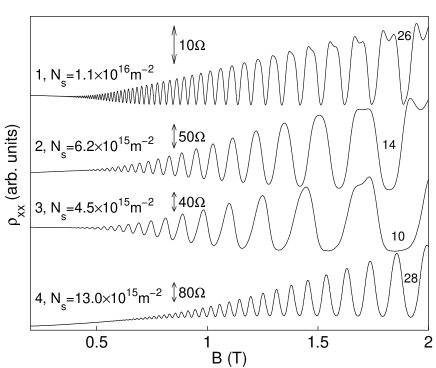
A magnetic field was applied perpendicular to the sample surface. The magnetoresistance of the 4 samples at 1.7 K is displayed in Fig. 1. We have measured the samples at temperatures down to 100 mK and found no significant improvement of the SdH oscillations, in agreement with expectations based on estimates of the Landau level broadening. Oscillations can be resolved down to magnetic fields of 0.15 T and filling factors up to 200. All observed features can be analyzed with one single SdH period with very high accuracy. From the largest filling factors that we can observe we estimate the Landau level width to about 0.4 meV.
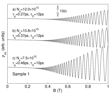
An expected zero-field spin splitting should depend on the effective electric field across the quantum well. Since we found it difficult to fabricate reliably functioning gates, we varied the carrier density and with it the effective electric field in the 2DEG via the persistent photoconductivity effect [15]. We used a red LED to illuminate the sample. Since we estimate the effective electric field to be largest in samples 1 and 4, we focus the following discussion on these samples. Figure 2 displays magnetoresistance traces obtained on sample 1 for three different carrier densities tuned via illumination with light. The data was taken after the light was switched off and the carrier density was stable as a function of time. The Drude scattering time as obtained from the resistivity at B=0 as well as the quantum scattering time from the magnetic field dependence of the SdH amplitude are also given for each resistance trace.
The electron density in InAs quantum wells can also be changed by hydrostatic pressure [16]. We reduced the carrier density in sample No. 4 by almost a factor of two via application of pressure up to and did again not find any beating pattern in the low-field SdH oscillations (not shown).
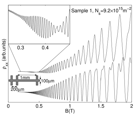
However, in some samples, in which the carrier density could be tuned with light, we found a beating pattern right after the illumination. Usually, after waiting for some time of the order of an hour the beating pattern was gone. In a few cases the beating pattern remained constant on the time scales of the experiment. Figure 3 shows resistance traces for sample 1 after the sample has been illuminated with an infrared LED and then kept in the dark for more than 24 hours. In this stage the resistivity of the sample changed by less than per hour. The magnetoresistance across two voltage probes separated by 1 mm clearly displays a weak beating pattern. A measurement taken at the same sample at the same time for voltage probes separated by only 200 m shows a perfectly one-period SdH pattern. Upon further illumination the beating pattern disappeared. We can observe such effects very rarely and only for special voltage contacts and illumination doses.
There seems to be at least qualitative agreement between experiment and theory on InAs wells with GaSb barriers [3, 4] and other material systems [5, 7, 8]. Our data obtained on InAs quantum wells with AlGaSb barriers with a large Al content as well as the data by Hopkins et al. [12] indicating the absence of SdH beating within the experimental resolution cannot be explained within this framework. The magnitude of the spin splitting according to the theory of Rashba et al. [11] should depend on the effective electric field across the quantum well. In the following we estimate this value of the effective electric field for our quantum wells.
Both the surface states and any Te doping of the top barrier will introduce a strong transverse electric field into the wells, pointing towards the substrate side. If there were no other doping sources present, the field at the top of the well would be given by , where is the electron sheet concentration, and the InAs permittivity. The field would decay to zero at the bottom, interface, implying an average field of approximately . The background bulk doping in the InAs itself is negligible compared to the measured concentrations. However, part of the electron concentration in all samples is due to interface donors, and in sample 3 this is the only known source. If we assume that this contribution is symmetrical and has the same value in all samples, , we must subtract this value from the measured . The fields obtained in this way are given in the last row of Table I. If the interface donors were unsymmetrically distributed, the values in the Table would have to be adjusted by an amount depending on the magnitude and sign of the asymmetry, maximally , but probably much less.
With the possible exception of sample 3, all samples have large built-in asymmetries, with transverse electric fields estimated to range from to for Samples 4 and 1, down to nominally zero for sample 3. The uncertainties on these estimates are on the order , i.e. small compared to the range of values. It is extraordinarily unlikely that accidental effects would compensate the different asymmetries in all samples. The absence of the SdH beating in our samples as well as those of Hopkins et al. [12] suggests a more fundamental suppression mechanism, somehow associated with InAs/AlSb wells, but absent in GaAs/(Al,Ga)As wells, and even in InAs/GaSb wells. The data of Heida et al. [9] appear to contradict this hypothesis, but it may be important that even their work indicates significant discrepancies between experiment and theory.
A Fourier-transform of the SdH pattern of sample 1 indicates a resolution of our experiment of better than 1 meV for the possible detection of a beating phenomenon. This limit is comparable with the one obtained from the width of the Landau levels. We have self-consistently calculated [17] the conduction band profile and wave function based on the sample parameters and then calculated the expected spin splitting using Rashba‘s theory [11]. We found a value of about 5 meV in agreement with Refs. [18, 19, 20].
Let us now return to the light induced beating pattern as displayed in Fig. 3. As light changes the carrier density, it also changes the effective electric field across the well. If this were the underlying reason for the observed beating pattern one would expect that the beating pattern is present without light, disappears at some does of light as the potential well becomes symmetric and then appears again once the asymmetry points to the other direction. In our case, if we observe this feature at all in an experiment, the beating pattern is only present for a certain dose of light, it is absent for lower and higher carrier densities. These observations strongly hint at the fact that in our samples a beating pattern in the low-field SdH oscillations does not stem from an asymmetry induced Rashba-type interaction.
In the following we argue that the observed SdH beating pattern in Fig. 3 arises from an inhomogeneous carrier distribution induced by the illumination. The light is not distributed homogenously along the Hall geometry and might therefore lead to an inhomogeneous carrier distribution. If a reasonable number of areas of different carrier density occur along the current path of the Hall geometry this could lead to a beating pattern of the low-field SdH oscillations. After the carriers have had enough time to relax back to thermal equilibrium the inhomogeneities and with it the beating pattern disappear. The time scales of the non-persistent photoconductivity effect are of the order of hours and are consistent with the disappearance of the beating pattern.
The importance of sample inhomogeneities obviously depends on the length scale of the experiment. The data in Fig. 3 suggest that over short length scales, in this case 200 m, the sample is homogeneous within the experimental resolution and therefore displays single period SdH oscillations. For a larger length scale of 1 mm the beating pattern is experimentally observed. We find roughly 21 oscillations between two nodes of the beating. If interpreted in terms of sample inhomogeneities this leads to a value of , which is not an unreasonable number.
While we do not question the valid interpretion of other experiments in terms of the Rasha-type spin orbit splitting, our experimental results cannot be explained within this framework. It is not clear why in our InAs-AlSb quantum wells the low-field SdH beating cannot be observed.
We do not know why our samples behave differently compared to Ref. [9] but like to stress that our sample quality is higher in terms of scattering times and electron mobilities. We do not expect to observe Berry phase-type effects in our samples [21] induced by strong Rashba-type spin orbit interaction.
From Fig. 1 it is obvious that spin splitting of SdH oscillations can be observed at magnetic fields as low as . The magnitude of the g-factor in our quantum wells can be determined by temperature dependent measurements or via experiments where the magnetic field in tilted with respect to the sample surface. We find in both cases values for the g-factor of [22]. This makes InAs-AlSb quantum wells promising candidates for spin-related experiments.
The fact that we do not observe a beating of the low-field SdH oscillations comes as a surprise and is completely unexpected. While spin-orbit interaction in general could still play a substantial role in these systems the contribution of the quantum well inversion asymmetry to it is likely to be small. This, however, could be an advantage for the possible realization of coupled spin states in quantum dots. [23]
We are grateful to T. Heinzel and S. Ulloa for helpful discussions and thank ETH Zürich and QUEST for financial support.
REFERENCES
- [1] D. Stein, K. von Klitzing, and G. Weimann, Phys. Rev. Lett. 51, 130 (1983)
- [2] H. L. Stormer, Z. Schlesinger, A. Chang, D. C. Tsui, A. C. Gossard, and W. Wiegmann, Phys. Rev. Lett. 51, 126 (1983)
- [3] J. Luo, H. Munekata, F. F. Fang, and P. J. Stiles, Phys. Rev. B 38, 10142 (1988)
- [4] J. Luo, H. Munekata, F. F. Fang, and P. J. Stiles, Phys. Rev. B 41, 7685 (1990)
- [5] B. Das, D. C. Miller, S. Datta, R. Reifenberger, W. P. Hong, P. K. Bhattacharya, J. Singh, and M. Jaffe, Phys. Rev. B 39, 1411 (1989)
- [6] M. Schultz, F. Heinrichs, U. Merkt, T. Colin, T. Skauli, and S. Lovold, Semicond. Sci Technol. 11, 1168 (1996)
- [7] J. Nitta, T. Akazaki, H. Takayanagi, and T. Enoki, Phys. Rev. Lett. 78, 1335 (1997)
- [8] G. Engels, J. Lange, Th. Schäpers, and H. Lüth, Phys. Rev. B 55, 7685 (1997)
- [9] J. P. Heida, B. J. van Wees, J. J. Kuipers, T. M. Klapwijk, and G. Borghs, Phys. Rev. B 57, 11911 (1998)
- [10] J. P. Lu, J. B. Yau, S. P. Shukla, M. Shayegan, L. Wissinger, U. Rössler, and R. Winkler, Phys. Rev. Lett. 81, 1282 (1998)
- [11] E. I. Rashba, Fiz. Tverd. Tela (Leningrad), 2, 1224 (1960), [Sov. Phys. Solid State 2, 1109 (1960)] 57, 11911 (1998)
- [12] P. F. Hopkins, A. J. Rimberg, R. M. Westervelt, G. Tuttle, and H. Kroemer, Appl. Phys. Lett. 58, 1428 (1991)
- [13] G. Tuttle, H. Kroemer, and J. H. English, J. Appl. Phys. 67, 3023 (1990); H.-R. Blank, M. Thomas, K. C. Wong, and H. Kroemer, Appl. Phys. Lett. 69, 2080 (1996)
- [14] C. Nguyen, B. Brar, H. Kroemer, and J. H. English, J. Vac. Sci. Technol. B 10, 898 (1992) and 11, 1706 (1993)
- [15] C. Gauer, J. Scriba, A. Wixforth, J. P. Kotthaus, C. Nguyen, G. Tuttle, J. H. English, and H. Kroemer, Sem. Science and Tech. 8, 137 (1993)
- [16] S. Brosig, K. Ensslin, B. Brar, M. Thomas, and H. Kroemer, Physica E 2, 214 (1998)
- [17] The use of G. Snider‘s Schrödinger-Poisson solver is gratefully acknowledged (http://www.nd.edu/ gsnider/)
- [18] G. Lommer, F. Malcher, and U. Rössler, Phys. Rev. B 32, 6965 (1985)
- [19] G. Lommer, F. Malcher, and U. Rössler, Phys. Rev. Lett. 60, 728 (1988)
- [20] E. A. De Andrada E Silva, G. C. La Rocca, and F. Bassani, Phys. Rev. B 50, 8523 (1994)
- [21] A. F. Morpungo, J. P. Heida, T. M. Klapwijk, B. J. van Wees, and G. Borghs, Phys. Rev. Lett. 80, 1050 (1998)
- [22] S. Brosig, K. Ensslin, B. Brar, M. Thomas, and H. Kroemer, Physica B 256-258, 239 (1998)
- [23] D. Loss and D. P. DiVincenzo, Phys. Rev. A 57, 120 (1998)
| Sample | ||||
|---|---|---|---|---|
| UCSB ID | ||||
| Distance of InAs well to surface (nm) | ||||
| Cap material | ||||
| Electron Density (m-2) | ||||
| Electron mobility (m2/Vs) | ||||
| Drude scattering time (ps) | ||||
| Quantum scattering time (ps) | ||||
| Estimated el. field (V/m) |