Photon assisted tunneling in a superconducting SET transistor induced by the Josephson oscillations of a SQUID
Abstract
Josephson oscillations generated by a SQUID were used to measure photon assisted tunneling in a superconducting single electron tunneling (SET) transistor. The SQUID was fabricated only a few microns from the SET transistor. The close proximity of the generator to the SET transistor allowed for a continuous sweep of the excitation frequency from 10 GHz to 190 GHz. The amplitude of the Josephson oscillations were tuned by adjusting the flux through the SQUID loop while the frequency was independently adjusted by controlling the bias voltage across the SQUID. Current peaks which could be attributed to photon assisted tunneling in the SET transistor were observed for bias voltages less than .
pacs:
85.25.Cp, 73.23.Hk, 74.50.+r, 85.30.WxMany artificially structured microsystems such as quantum dots or single-electron tunneling transistors have characteristic energies on the order of 1 meV. The frequencies needed to probe these energies spectroscopically are tens to hundreds of GHz. This is an inconvenient frequency range since there are few tunable sources of radiation available in this range which can be coupled to a sample at low temperature while isolating the sample from room temperature blackbody radiation.
One suitable radiation source is a Josephson junction. When a Josephson junction is biased above the critical current, voltage oscillations appear with a frequency , where is the dc voltage across the junction. By adjusting the average voltage across the junction, the frequency of these oscillations can be tuned. We have used such Josephson oscillators to measure photon assisted tunneling in a superconducting single electron tunneling (SET) transistor.
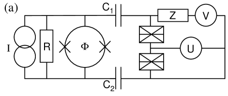
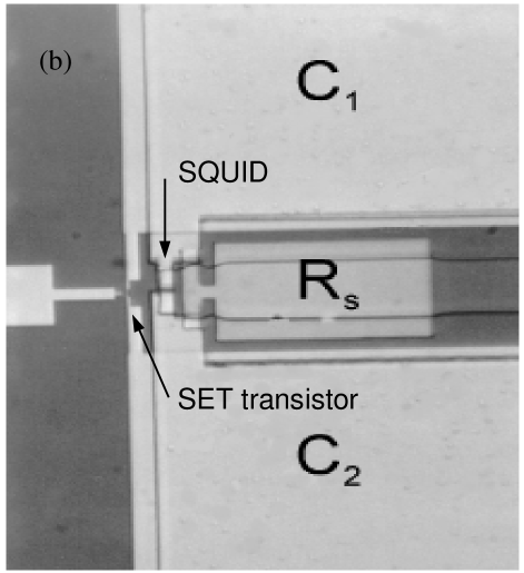
In the experiments, two Al/AlOx/Al Josephson junctions were used in parallel as in a superconducting quantum interference device (SQUID). Normally SQUIDs are used to measure magnetic flux but in this case we used the flux modulation of the critical current of the SQUID to tune the power of the radiation that was generated. The SQUID loop formed by the two junctions was 10 m2 resulting in an inductance of about 3 pH. The Josephson junctions had critical currents of 1 A and were shunted by a 30 Pt shunt. Figure 1a shows a schematic diagram of the circuit and Fig. 1b is an electron microscope image of the sample showing the coupling capacitors and and the positions of the SET transistor and the SQUID. The generator was located just 10 m from the SET transistor.
It was possible to tune the frequency of the Josephson oscillations continuously from 10 GHz to 190 GHz. An essential feature of this experiment is that the entire circuit is smaller than a wavelength at all relevant frequencies. This means that the coupling of the radiation from the generator to the sample circuit was not strongly frequency dependent as is typically the case with larger circuits where microwave resonances affect the coupling. Another advantage of the small size of the circuit is that the entire circuit could be placed in a microwave tight enclosure with filtered dc feedthroughs. This prevents blackbody radiation in the GHz range from interfering with the experiment. The frequency and amplitude of the SQUID generator were adjusted with dc signals and the detection current flowing through the SET was also a dc signal.
Because the impedance of the SQUID is much smaller than the resistance of the SET transistor, the SQUID generator can best be modeled as an rf voltage source with a source impedance equal to the resistive shunt. The SQUID generates an rf voltage, [1]
| (1) |
Here is the critical current of the SQUID, is the SQUID bias current, is the shunt resistance, and .
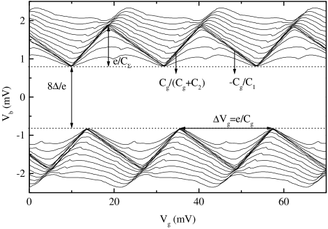
The SET transistor consisted of two low capacitance Al/AlOx/Al tunnel junctions in series. Since these junctions were much smaller than the junctions in the SQUID, it was necessary to fabricate the SET junctions in a separate fabrication step from the SQUID junctions. [2] The junctions had capacitances of = 52 aF and = 95 aF, resistances of = 400 k and = 90 k, and a gate capacitance of = 7.3 aF. A contour map of the current through the SET transistor as a function of gate voltage and bias voltage in the absence of applied radiation is shown in Fig. 2. Very little current was observed for bias voltages less than . No supercurrent was observed because of the high resistance of the sample and the Josephson-quasiparticle cycle[3] was not observed because . Here
is the total capacitance of the island. There is a fairly sharp onset of current that corresponds to the threshold for sequential quasiparticle tunneling in the SET transistor. This threshold forms the zigzag pattern that appears between and in Fig. 2.
When a bias voltage is applied across the SQUID,
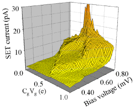
Josephson oscillations occur which enable additional tunnel processes through the SET transistor via photon assisted tunneling. [4, 5] Figure 3 shows the current through the SET transistor when 55 GHz radiation is applied. The threshold for sequential quasiparticle tunneling corresponds to the sharp rise of current at bias voltages at 0.8 mV. The two higher plateaus arise from photon assisted tunneling through one of the junctions and then direct tunneling through the other junction. The lower plateau is due to photon assisted tunneling through both junctions.
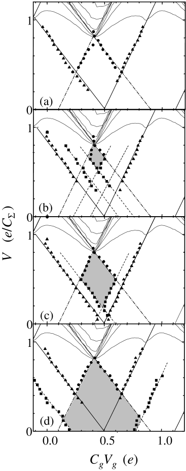
Figure 4 shows the positions of the thresholds for photon assisted tunneling for four frequencies (0 GHz, 30 GHz, 79 GHz, and 160 GHz) in the plane. Currents above 100 pA are plotted as contours and the positions of smaller current peaks and thresholds are plotted as solid points. The gray diamond shaped regions indicate where each quasiparticle is assisted by one photon in tunneling through each junction. This corresponds to the lower diamond-shaped plateau in Fig. 3. A constant voltage across junction 1 corresponds to a line with a slope of in the plane and a constant voltage across junction 2 correspond to a line with a slope of in the plane. For this reason the thresholds all follow lines with these slopes. The positions of the photon assisted tunneling thresholds correspond to a constant voltage across one of the junctions that is less than the voltage at which the original threshold occurs. Here is an integer that indicates the order of the photon assisted tunneling peak.
Figure 4a shows the current when no microwave radiation is applied. In addition to the threshold for the
sequential tunneling of quasiparticles, small current peaks occur when the BCS density of states of the island and one of the leads aligns. These current peaks arise from the tunneling of thermally activated quasiparticles in a process known as singularity matching[6] and are indicated by the triangles. A line of current peaks was also observed when the voltage across one of the junctions equals . If the bias across a junction is greater than , then tunneling can proceed through that junction at the normal rate. These current peaks are indicated by the circles.
Figures 4b-4d show the current through the SET transistor when high frequency radiation from the SQUID is applied. Again the solid triangles represent the singularity matching peaks and the circles represent the transition to normal rate tunneling in one of the two junctions. The solid squares represent the thresholds for photon assisted tunneling. These squares line along the dotted lines which indicate the positions of thresholds for photon assisted tunneling that are expected for the frequency of the radiation applied. The thresholds for sequential quasiparticle tunneling and for singularity matching do not move as a function of frequency but the thresholds for photon assisted tunneling scale linearly with frequency.
Photon assisted tunneling should also show a characteristic scaling as a function of rf power. The amplitude of the th order peak should modulate as , where is the th order Bessel function.[7] In the experiment, the zeroth order peak decreases and the higher order peaks increase as the power increases as would be expected from the Bessel function relations at low rf
powers. However, the power generated by the SQUID was not sufficient to see the amplitude of the peaks oscillate as one would expect for high rf powers. From Eqn. 1, one can estimate that the amplitude of the rf signal should be approximately = 30 V. The maximum amplitude of the rf voltage that a SQUID can deliver is limited by the product of the Josephson junctions. Since the product for overdamped aluminum junctions is limited to about 0.1 mV, these Josephson generators will not generate enough power to observe oscillations in the amplitude of the photon assisted tunneling peaks for frequencies higher than about 3 GHz. Higher microwave powers could be achieved by using arrays of junctions or other materials. Typical products for overdamped niobium or high junctions are about 1 mV. This leads to oscillations in the amplitude of the photon assisted tunneling peaks for frequencies up to about 30 GHz for single junction oscillators.
In conclusion, high frequency oscillations generated by a SQUID were used to irradiate a superconducting SET transistor. This radiation induced photon assisted tunneling in the SET transistor over a span of frequencies from 10 GHz to 190 GHz. A linear scaling with the frequency was observed. An advantage of using SQUIDs as the rf source is that microwave resonances in the measurement circuit were not observed so that it was possible to tune the frequency continuously. Placing the rf oscillator on the same chip as the sample to be measured also makes it possible to enclose the entire measurement circuit in a microwave tight box which minimizes external interference such as the blackbody radiation of room temperature equipment.
Acknowledgements.
Support from Esprit project 22953, CHARGE, is gratefully acknowledged.REFERENCES
- [1] K. K. Likharev, Dynamics of Josephson Junctions and Circuits Gordon and Breach, New York, p. 92 (1986).
- [2] E. H. Visscher, S. M. Verbrugh, J. Lindeman, P. Hadley and J.E. Mooij, Appl. Phys. Lett. 66 305 (1995).
- [3] T. A. Fulton, P. L. Gammel, D. J. Bishop, L. N. Dunkleburger, and G. J. Dolan, Phys. Rev. Lett. 63 1307 (1989).
- [4] Y. Nakamura, C. D. Chen, and J. S. Tsai, Czech. J. Phys. 46 2301 (1996).
- [5] R. J. Fitzgerald, J. M. Hergenrother, S. L. Pohlen, and M. Tinkham, Phys. Rev. B 57 9893 (1998).
- [6] Y. Nakamura, A. N. Korotkov, C. D. Chen, and J. S. Tsai, Phys. Rev. B. 56 5116 (1997).
- [7] P. K. Tien and J. P. Gordon, Phys. Rev. 129 647 (1963).