Hall Voltage with the Spin Hall Effect
Abstract
The spin Hall effect does not generally result in a charge Hall voltage. We predict that in systems with inhomogeneous electron density in the direction perpendicular to main current flow, the spin Hall effect is instead accompanied by a Hall voltage. Unlike the ordinary Hall effect, we find that this Hall voltage is quadratic in the longitudinal electric field for a wide range of parameters accessible experimentally. We also predict spin accumulation in the bulk and sharp peaks of spin-Hall induced charge accumulation near the edges. Our results can be readily tested experimentally, and would allow the electrical measurement of the spin Hall effect in non-magnetic systems and without injection of spin-polarized electrons.
pacs:
72.25.Dc, 71.70.EjCurrently, much attention is given to studies of the spin Hall effect, which allows to polarize electron spins without magnetic fields and/or magnetic materials natureSHC ; r0 ; r1 ; r2 ; r3 ; Rashba ; Rashba1 ; r4 ; r5 ; r6 ; r7 ; r8 ; r9 ; r10 ; Kato ; Wunderlich ; Valenzuela . In the spin Hall effect, electrically induced electron spin polarization accumulates near the edges of a channel and is zero in its central region. This effect is caused by deflection of carriers moving along an applied electric field by extrinsicr1 and/or intrinsicr3 mechanisms. In a non-magnetic homogeneous system, spin accumulation is not accompanied by a charge Hall voltage because two spin Hall currents cancel each other natureSHC . The absence of Hall voltage leads to difficulties in probing the spin Hall effect, since measuring a charge accumulation is much easier than measuring a spin accumulation. Recently, the spin Hall effect has been observed both optically Kato ; Wunderlich and electrically Valenzuela . In the latter case, a charge accumulation has been created through injection of spin-polarized electrons into the sample Valenzuela .
In the present Letter, we predict that in a system with an inhomogeneous electron density profile in the direction perpendicular to the direction of main current flow, the spin Hall effect results in both spin and charge accumulations. The pattern of charge accumulation is determined by the interplay of two mechanisms. The first mechanism of charge accumulation is based on the dependence of spin-up and spin-down currents on local spin-up and spin-down densities. Spin currents, outgoing from regions with higher densities, are not fully compensated by incoming currents, therefore, a charge accumulation appears. This mechanism is primarily responsible for the non-zero Hall voltage. The second mechanism of charge accumulation is related to scattering of spin currents on sample boundaries which act like obstacles. Like in the case of Landauer resistivity dipoles Landauer , this scattering leads to formation of local charge accumulation, which is also expected in traditionally-studied spin Hall systems. In addition, we show that in systems with inhomogeneous electron density the spin accumulation appears not only near the sample boundaries, but also in the bulk. Our approach does not involve any use of magnetic materials and fields, therefore, the spin Hall effect can be measured electrically in completely non-magnetic system and without injection of spin-polarized electrons.
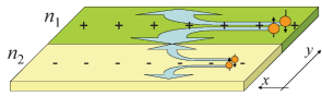
To illustrate this effect, let us begin by considering a system having a step profile of electron density, as shown in Fig. 1. There are several possible ways to fabricate such a system including density depletion by an electrode, inhomogeneous doping YP , or variation of the sample height. What is important for us is that the perpendicular (in direction) spin currents are different in the regions with different electron density. Then, if we consider currents passing through the boundary separating regions with different charge densities ( and ), it is clear that the spin current from the region with higher electron density has a larger magnitude than the current in the reverse direction. The difference in currents implies charge transfer through the boundary and formation of a dipole layer.
Let us now provide a quantitative analysis of this effect. We employ a two-component drift-diffusion model flatte ; PDV , and in order to find a self-consistent solution, we supplement the drift-diffusion equations with the Poisson equation. In our drift-diffusion calculation scheme, the inhomogeneous charge density profile is defined via an assigned positive background density profile (such as the one in Fig. 1), which, as discussed above, can be obtained in different ways. Assuming homogeneous charge and current densities in direction and homogeneous -component of the electric field in both and directions, we can write a set of equations including only and dependencies:
| (1) |
| (2) |
and
| (3) |
where is the electron charge, is the density of spin-up (spin-down) electrons, is the current density, is the spin relaxation time, is the spin-up (spin-down) conductivity, is the mobility, is the diffusion coefficient, is the permittivity of the bulk, and is the parameter describing deflection of spin-up (+) and spin-down (-) electrons. The current in -direction is coupled to the homogeneous electric field in the same direction as . The last term in Eq. (2) is responsible for the spin Hall effect.
Equation (1) is the continuity relation that takes into account spin relaxation, Eq. (2) is the expression for the current in direction which includes drift, diffusion and spin Hall effect components, and Eq. (3) is the Poisson equation. It is assumed that , , and are equal for spin-up and spin-down electrons. prec In our model, as it follows from Eq. (2), the spin Hall correction to spin-up (spin-down) current (the last term in Eq. 2) is simply proportional to the local spin-up (spin-down) density. All information about microscopic mechanisms for the spin Hall effect is therefore lumped in the parameter .
Combining equations (1) and (2) for different spin components we can get the following equations for electron density and spin density imbalance :
| (4) |
and
| (5) |
Analytical solution – Before solving Eqs. (3)-(5) numerically, let us try to find analytical solutions in specific cases. This will help us in the discussion of the numerical results. An analytical steady-state solution of these equations can indeed be found for the case of exponential density profile in a system which is infinite in the direction.
The structure of Eqs. (3)-(5) allows us to select a solution in the form
| (6) | |||
| (7) | |||
| (8) |
where , and are constants ( and are assigned). This solution corresponds to constant spin polarization . Substituting Eqs. (6)-(8) into Eqs. (4) and (5) (note that the Poisson equation (3) is automatically satisfied) we obtain
| (9) | |||
| (10) |
From these equations, eliminating , we find
| (11) |
The physical solution corresponds to the + sign in Eq. (11). It can be easily verified that the solution given by Eqs. (6)-(8), (11) corresponds to . Substituting Eq. (11) into Eq. (9) we finally get
| (12) |
The second term on the RHS of Eq. (12) is the electric field needed to compensate the transverse current arising due to the spin Hall effect. If we now assume the sample has a finite (but large) width , then, this term can be interpreted as due to charge accumulation near the edges, as in the ordinary Hall effect. Therefore, the Hall voltage can be written as
| (16) |
From this equation we see that the Hall voltage is quadratic in for small values of the parameter , and linear in for large values of this parameter. In fact, the quadratic dependence is quite unusual, since in the ordinary Hall effect the Hall voltage is linear in the longitudinal current. The reason for this unusual dependence can be understood as follows. The charge current in the direction, determined by the difference of spin-up and spin-down currents, has a component (related to the last term in Eq. (2)) proportional to the spin density imbalance times . At small values of , the spin density imbalance is proportional to itself. Therefore, the charge current and Hall voltage are quadratic in . At large values of , the spin density imbalance saturates and the current dependence on becomes linear. Another difference with respect to the ordinary Hall effect is that the polarity of the Hall voltage in the spin Hall effect is fixed by the geometry of the structure, and does not depend on the direction of the longitudinal current.
Let us now estimate the magnitude of . Taking parameters related to experiments on GaAs (ns, (Ref. Rashba, ), cm2/(Vs), V/cm, , m), we find . Therefore, in experiments with GaAs, most likely, a quadratic Hall voltage dependence on the longitudinal electric field can be observed.
Numerical solution – Equations (3)-(5) can be solved numerically for any reasonable form of . We choose for their simplicity (and possibility to be realized in practice) a step profile and an exponential profile. We solve these equations iteratively, starting with the electron density close to and close to zero and recalculating at each time step. prec1 Once the steady-state solution is obtained, the Hall voltage as a function of is calculated as a change of the electrostatic potential across the sample.
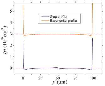
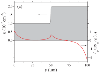
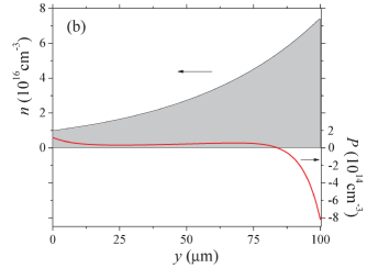
Fig. 2 shows distributions of the charge density and spin density imbalance in systems with a step (panel (a) of Fig. 2) and exponential (panel (b) of Fig. 2) background densities. The values of parameters used for these particular simulations were selected to be close to experimental conditions reported in Ref. Kato, . However, we have tested the robustness of our predictions by solving Eqs. (3)-(5) for different values of parameters, and found that the predicted Hall voltage should be measurable under a wide range of experimental parameters. Quite generally, the self-consistent charge density is very close to the background density . Small deviations of from can be observed in regions with strong gradients of . In particular, we can notice that the step profile of electron density in Fig. 2(a) is smoothed out. Such a charge redistribution is related to the diffusion term in Eq. (4). The charge diffusion leads to the formation of a built-in electric field that equilibrates the charge diffusion.
We also find that the induced spin density imbalance in systems with inhomogeneous electron densities shows some new features, in addition to the well-known spin accumulation near the edges. For instance, in Fig. 2(a), has an additional peak around m. In Fig. 2(b), is almost constant in the central region of the sample. In both cases, the physics of non-zero spin density imbalance is the same: the spin-current incoming from the right is stronger than the spin-current incoming from the left. We note that the integral spin density imbalance is always zero.
At , the system is spin-unpolarized and there is no Hall voltage. When the longitudinal current is switched on, the electron charge redistributes, and the associated Hall voltage appears. The change of electron density due to the spin Hall effect is presented in Fig. 3. The first interesting observation is that there is a strong charge accumulation near the edges followed by a charge depletion region. Another observation is that the total electron density in the left region of the samples (m) has increased and, correspondingly, the total electron density in the right region has decreased. This change of the electron distribution can be seen in Fig. 3. Therefore, the left part of the samples is charged negatively and the right part is charged positively, as schematically shown in Fig. 1.
The mechanism of formation of sharp peaks of charge accumulation near the edges is similar to the mechanism of formation of Landauer resistivity dipoles Landauer . From the point of view of spin currents, the sample edges act as obstacles which block the current flow, and lead to charge accumulation. The adjacent regions with the depleted electron density can be interpreted as screening clouds. We stress that this Landauer-type dipoles of charge accumulation are quite general for spin Hall systems, and should thus be present also in traditionally studied structures with a constant density profile.
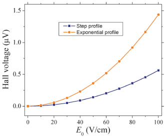
We finally plot in Fig. 4 the change of the electrostatic potential across the sample as a function of longitudinal electric field. The Hall voltage, for both density profiles, has a dependence on which is very close to the exponential dependence we have predicted analytically in Eq. 16 for small values of . The fact that this exponential dependence appears also in the step profile, hints at a possible “general” property of the Hall voltage in spin Hall systems with inhomogeneous densities. We emphasize that a Hall voltage should also appear in spin Hall systems with a homogeneous electron density, but inhomogeneous . This corresponds to the case in which the spin-orbit coupling is dependent on spaceserra ; nitta .
In conclusion, we have shown that a Hall voltage would appear in spin Hall systems with inhomogeneous electron density in the direction perpendicular to main current flow. The striking result is that this Hall voltage is generally quadratic in the longitudinal electric field, unlike the ordinary Hall voltage which is linear in the same field. These results can be easily verified experimentally, and would simplify tremendously the measurement of the spin Hall effect by allowing an electrical measurement of the latter in non-magnetic systems, and without injection of spin-polarized electrons.
This work is partly supported by the NSF Grant No. DMR-0133075.
References
- (1) J. Inoue and H. Ohno, Science 309, 2004 (2005).
- (2) M. I. D’yakonov and V. I. Perel, Phys. Lett. A 35, 459 (1971).
- (3) J. E. Hirsch, Phys. Rev. Lett. 83, 1834 (1999).
- (4) S. Murakami, N. Nagaosa, S.-C. Zhang, Science 301, 1348 (2003).
- (5) J. Sinova, D. Culcer, Q. Niu, N. A. Sinitsyn, T. Jungwirth, and A. H. MacDonald, Phys. Rev. Lett. 92, 126603 (2004).
- (6) H.-A. Engel, B. I. Halperin, and E. I. Rashba Phys. Rev. Lett. 95, 166605 (2005).
- (7) H.-A. Engel, E. I. Rashba, and B. I. Halperin Phys. Rev. Lett. 98, 036602 (2007).
- (8) J. Inoue, G. E. W. Bauer, and L. W. Molenkamp, Phys. Rev. B 70, 041303(R) (2004).
- (9) B. A. Bernevig and S.-C. Zhang, Phys. Rev. Lett. 95, 016801 (2005).
- (10) M. W. Wu and J. Zhou, Phys. Rev. B 72, 115333 (2005).
- (11) E. M. Hankiewicz, G. Vignale, and M. E. Flatté, Phys. Rev. Lett. 97, 266601 (2006).
- (12) B. K. Nikolić, S. Souma, L. P. Zârbo, and J. Sinova, Phys. Rev. Lett. 95, 046601 (2005).
- (13) J. I. Inoue, G. E. W. Bauer, L. W. Molenkamp, Phys. Rev. B 70, 041303(R) (2004).
- (14) A. G. Mal’shukov and C. S. Chu, Phys. Rev. Lett. 97, 076601 (2006).
- (15) Y. K. Kato, R. C. Myers, A. C. Gossard, D. D. Awschalom, Science 306, 1910 (2004).
- (16) J. Wunderlich, B. Kaestner, J. Sinova, and T. Jungwirth, Phys. Rev. Lett. 94, 047204 (2005).
- (17) S. O. Valenzuela and M. Tinkham, Nature 442, 176 (2006).
- (18) R. Landauer, IBM J. Res. Develop. 1, 223 (1957).
- (19) Y. V. Pershin and V. Privman, Phys. Rev. Lett. 90, 256602 (2003).
- (20) Z. G. Yu and M. E. Flatté, Phys. Rev. B 66, 201202 (2002).
- (21) Y. V. Pershin and M. Di Ventra, cond-mat/0701678.
- (22) This is a good approximation for the range of parameters considered in this work.
- (23) We have employed the Scharfetter-Gummel discretization scheme [D. L. Scharfetter and H. K. Gummel, IEEE. Trans. Electron. Devices, ED-16, 64 (1969)] to solve both Eqs. (4) and (5) numerically.
- (24) M. Valín-Rodríguez, A. Puente, and L. Serra Phys. Rev. B 69, 153308 (2004).
- (25) J. Nitta, T. Akazaki, and H. Takayanagi, Phys. Rev. Lett. 78, 1335 (1997).