Construction of a Versatile Ultra-Low Temperature Scanning Tunneling Microscope
Abstract
We constructed a dilution-refrigerator (DR) based ultra-low temperature scanning tunneling microscope (ULT-STM) which works at temperatures down to 30 mK, in magnetic fields up to 6 T and in ultrahigh vacuum (UHV). Besides these extreme operation conditions, this STM has several unique features not available in other DR based ULT-STMs. One can load STM tips as well as samples with clean surfaces prepared in a UHV environment to an STM head keeping low temperature and UHV conditions. After then, the system can be cooled back to near the base temperature within 3 hours. Due to these capabilities, it has a variety of applications not only for cleavable materials but also for almost all conducting materials. The present ULT-STM has also an exceptionally high stability in the presence of magnetic field and even during field sweep. We describe details of its design, performance and applications for low temperature physics.
I INTRODUCTION
The scanning tunneling spectroscopy (STS) technique by use of scanning tunneling microscope (STM) has become important for studies of low temperature physics in recent years. The STS is a powerful method to investigate local electronic density of states (LDOS) of material surfaces with high spatial ( nm) and energy resolutions ( meV) at cryogenic temperature below 10 K. Potentially, there are many applications in that temperature range, for example, unconventional superconductors with low transition temperatures (), quantum nanostructures on semiconductor surfaces, . In principle, we can expect better performance of STS at lower temperatures because of smaller thermal broadenings of tunnel spectra and thermal expansion coefficients of materials. So far, several STMs that work at sub-Kelvin temperatures have been constructed; for example, 3He refrigerator based STMs ( K) pan ; geneve ; hamburg and dilution refrigerator (DR) based STMs ( K) hess ; tsukuba ; delft ; cnrs ; madrid ; hanaguri . However, due to technical difficulties, none of the existing DR-based STMs has the full ultrahigh vacuum (UHV) compatibility with which one can prepare clean sample surfaces in situ. In other words, samples are limited only to cleavable materials or those with chemically inert surfaces for so far constructed STMs based on DR.
In this article, we describe details of design, construction and test results of a versatile ultra-low temperature STM (ULT-STM) which we have constructed recently ourSTM1 ; ourSTM2 . It works at triple extreme conditions, , at very low temperatures down to 30 mK, in high magnetic fields up to 6 T and in UHV. It has also the following unique features: one can (1) prepare clean sample surfaces in a UHV chamber, (2) load the samples and tips to an STM head keeping low temperature and UHV conditions, and then (3) cool them back to near the base temperature within 3 hours. Therefore, the ULT-STM has a variety of applications without being restricted only to cleavable materials such as layered ones bound by the van der Waals force. It has been successfully used, for example, in STS measurements of Landau quantization in two-dimensional electron systems at surfaces of semiconductors niimiinas and graphites matsuiprl ; niimipe ; niimiprl and of surface electronic states in a spin-triplet superconductor Sr2RuO4 kambara .
II DESIGN AND CONSTRUCTION
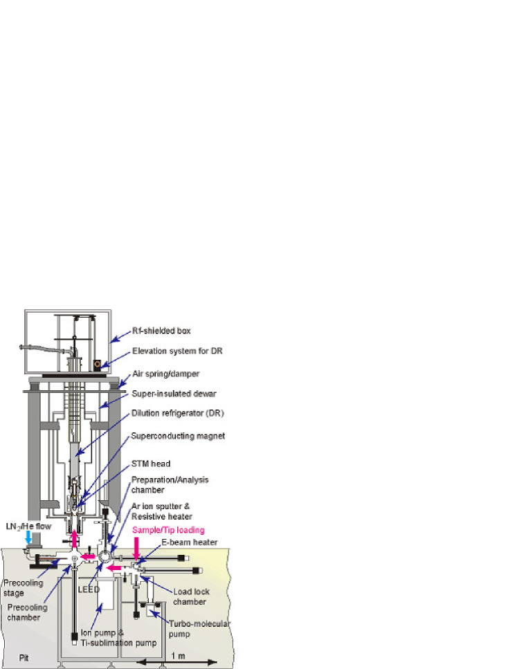
II.1 Cryostat with bottom-loading mechanism
For sample/tip exchange, we adopted the bottom-loading mechanism, instead of the ordinary top-loading one because of the following technical reasons. (1) One can shorten the access length for a sample/tip transfer rod. (2) A specially designed DR with a large-bore central access for top-loading is not necessary. UHV chambers for sample/tip preparations and evaluations are located on floor of an experimental pit of 1.5 m deep. The cryostat is hung from an anti-vibration table and connected with the UHV chambers at the bottom (Fig. 1). The central part of the cryostat is a commercial DR oxford with a super-insulated dewar. The volume of liquid helium reservoir (74 liters) is large enough to maintain the base temperature for almost 3 days without refilling liquid helium. A 6 T superconducting magnet with a 90 mm bore diameter is immersed in the liquid-helium bath and surrounds a UHV can (see Fig. 2). All electronic equipments such as a current preamplifier preamp and a controller stmcu for STM measurement are located in an rf-shielded box/room in order to eliminate electrical noises from outside.
II.2 STM head
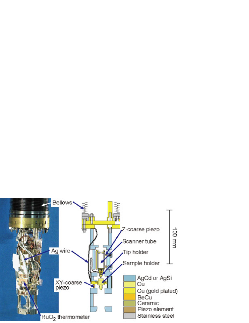
A photo and a cross-sectional view of the STM head unisokustm are shown in Fig. 3. The main body of the head is made of hard silver (Ag( 99 at.%)+Cd ( 1 at.%)) and silicon silver (Ag0.85Si0.15) rather than copper or copper-based alloys to prevent large nuclear-spin heat capacities in high magnetic fields at very low temperatures. These silver-based alloys have better mechanical strength compared to pure metals and proper thermal conductivity fukuyama . On the other hand, a sample stage, sample holder and tip holder are made of high purity copper for better thermalization and moderate mechanical strength. They are thermally linked to the mixing chamber (MC) of DR through annealed silver foils and wires (see next section).
The coarse approach of tip towards sample surface (Z-coarse approach) is obtained by the stick and slip motion with piezo actuators. Two of the actuators hold an inner ceramic tube, which contains a single-tube piezo scanner, on three sides of the triangular cross-section. The speed of Z-coarse approach is 60 m/s with an application of pulses of 150 V at 0.5 kHz at temperatures below 4 K.
The tip holder is fixed to one end of the piezo scanner with an M3 screw. The maximum XY scan area of the scanner is 1.51.5 m2 below 4 K, while 4.54.5 m2 at room temperature. The sample holder is also screwed into the sample stage with M12. Samples are glued onto the sample holder with silver epoxy. For thermometry, a RuO2 chip-resistor is attached to the sidewall of sample stage.
II.3 Thermal contacts and isolations
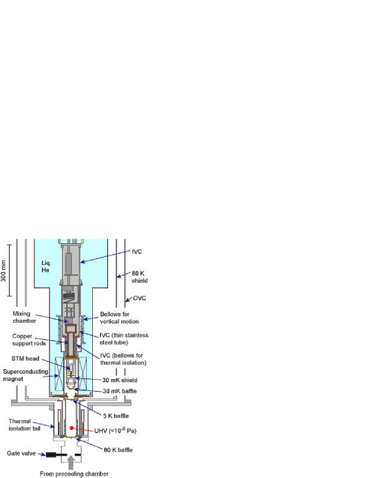
The UHV space for the STM head is separated from the vacuum space for DR. Therefore, the inner vacuum can (IVC) is made of thin-wall stainless steel tubes (0.5 mm thick) and welded bellows (0.12 mm thick) to reduce heat conduction from one end at 4 K to another at the base temperature (see Fig. 2). The STM head is rigidly supported from the bottom of the IVC and thermally connected to the MC with three support rods made of copper (8 mm in diameter and 168 mm long). The STM head is surrounded by a copper radiation shield with a demountable bottom cap which is thermally anchored to the MC.
The sample and tip are thermally anchored independently to the MC with additional well-annealed high-purity silver thin-foils and -wires. Mylar sheets (25 m thick) are inserted between the sample stage/tip holder and the silver thermal links for electrical isolation.
In order to minimize the access length for bottom loading, we made a specially designed attachment (thermal isolation tail) which separates the UHV space from the vacuum space for the dewar inside the outer vacuum can (OVC) (see Fig. 2). The thermal isolation tail consists of three coaxial cylinders to minimize heat leaks from higher temperature sides. Several parts of the inner and outer cylinders are made of thin-wall stainless-steel tubes (0.5 mm thick) and flexible tubes (0.15 mm thick). The middle cylinder made of copper is thermally anchored to the neck of the dewar ( K). Between the cylinders, 30–50 layers of aluminized Mylar sheets (super-insulation) are inserted for radiation shielding. Two demountable baffles thermally anchored to 5 K and 80 K shield radiation through the access line from the bottom.
To reduce heat leaks through electrical lead wires, we used two different kinds of wires in the IVC; a co-axial cable (inner conductor: superconducting NbTi wire of 0.1 mm in diameter, outer conductor: CuNi tube of 0.6 mm in diameter) for tunnel current detection or the bias voltage application and superconducting NbTi twisted-wires (each 0.10 mm in diameter) for the high voltage application to the piezo actuators. In the UHV space, all the wires are converted to insulated copper twisted-wires which are thermally anchored to the MC.
II.4 UHV chambers
The UHV chamber unisoku consists of three parts: (1) load-lock chamber, (2) preparation/analysis chamber, and (3) precooling chamber (see Fig. 1). The actual procedure of sample/tip preparation is as follows. At first we introduce a new sample or tip into the load-lock chamber and evacuate it below 10-5 Pa by a turbo molecular pump. The tip can be cleaned by electron beam heating, if necessary. Then it is transferred to the preparation/analysis chamber with a magnetic transfer rod. We can prepare a clean sample surface here by resistive heating and/or argon ion sputtering in a UHV environment ( Pa) achieved with an ion pump and a titanium sublimation pump (1600 ). The surface quality can be analyzed by low-energy electron diffraction (LEED). After the surface preparation, the sample/tip is transferred to a copper platform in the precooling chamber. Here it is cooled by liquid nitrogen or liquid helium flow down to 100 K or 7 K, respectively. The sample cleavage can be done at various temperatures between 7 and 300 K by pushing a small post glued on top of the sample with a blade in this chamber. Finally, the precooled sample/tip is transferred to the STM head.
II.5 Vibration isolation
The whole cryostat is suspended from the anti-vibration table with air springs, dampers (vertical direction) and rubber stacks (horizontal direction). Mechanical resonance frequencies of this system are 1.5 Hz in the vertical and 2.0/2.5 Hz in the horizontal directions, respectively. Four support pillars of the table are filled with sand for vibration damping. Vibrational and acoustic noises generated by vacuum pumps for DR operation are eliminated by installing them on a rigid frame with rubber springs and dampers in an acoustic shielded box. Soft bellows are inserted in pumping lines near the top of the cryostat. Especially, T-shaped bellows are used for the still pumping line (76 mm in diameter) of DR. To increase the rigidity of the DR unit in the IVC, we inserted additional thermal isolation supports between different temperature stages below the 1 K pot.
III TEST RESULTS
III.1 Sample/tip exchange
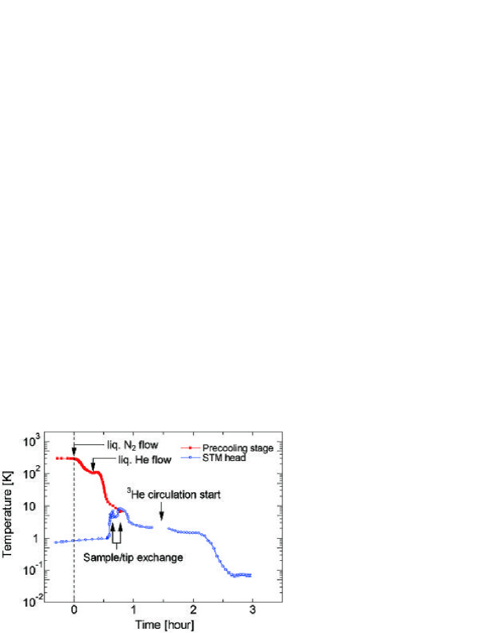
Figure 4 shows time evolutions of temperatures of the precooling stage and STM head during the sample/tip exchange procedure. Before inserting the sample/tip, we first stop the 3He circulation of DR. Although the STM head is warmed temporarily up to about 10 K by the insertion, it quickly cools back to 2 K due to a large heat capacity of 3He–4He mixture liquid in the DR unit. By restarting the 3He circulation, it cools back below 70 mK in only 1.5 hours. It takes about 15 hours more to reach the lowest temperature below 30 mK. The quick turnaround back to near the base temperature within 3 hours in total is one of extraordinary features of this ULT-STM.
III.2 Basic performance of the ULT-STM
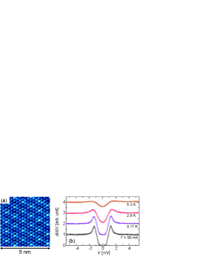
To demonstrate the basic performance of ULT-STM, we carried out test measurements using a 2H-NbSe2 sample. 2H-NbSe2 is a well-studied material in which the superconducting phase (=7.2 K) and the charge density wave (CDW) phase (=33 K) coexist. We used electrochemically etched W-wires as STM tips for these measurements.
Figure 5(a) shows a constant current image of a cleaved surface of 2H-NbSe2 at mK. The atomic corrugation of surface Se as well as the CDW modulation are clearly visible. In the spectroscopy mode, we measured a set of tunnel spectra averaged over a nm2 area at various temperatures (Fig. 5(b)). An expected temperature dependence of the superconducting energy gap is observed here. The modulation frequency used here is 511.7 Hz, and the modulation amplitude is 20 and 50 Vrms for K and K, respectively.
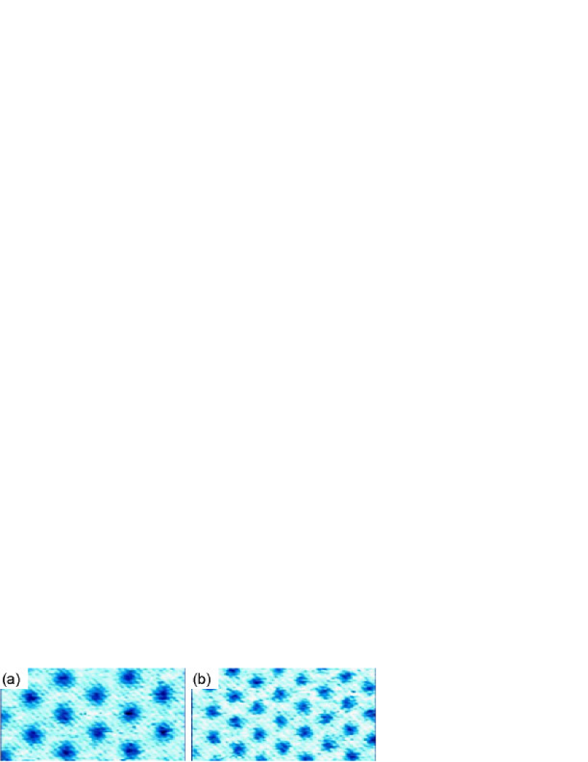
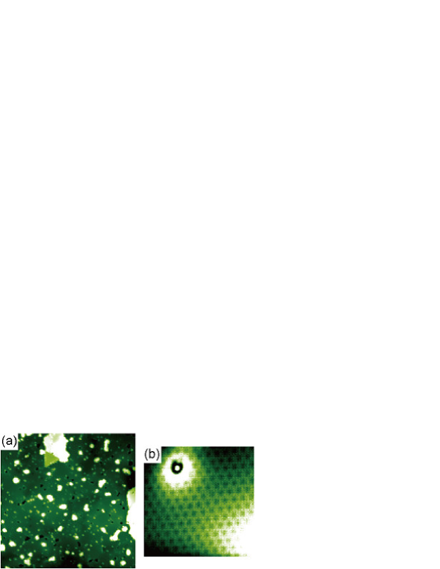
In Figs. 6(a)(b), we show images in the presence of magnetic fields of 0.2 and 0.4 T on the same sample surface as in Fig. 5. As the bias voltage is tuned at one of the coherence peaks of the gap structure for these images, the dark spots represent the vortex cores hess2 . Note that the scan area ( nm2) here is much larger than that ( nm2) in Fig. 5. The Abrikosov (triangular) lattices of the quantized vortices are formed without distortions.
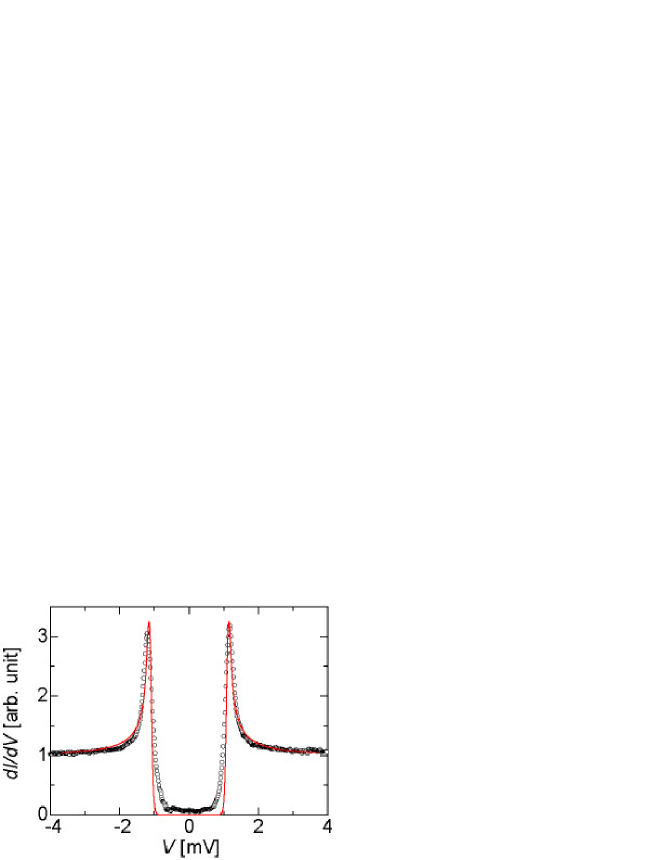
To evaluate the energy resolution in the tunnel spectroscopy (TS) mode quantitatively, we performed TS measurements of conventional superconductors such as Ta, Nb, . where the standard BCS theory is applicable. The normalized tunnel conductance () of a normal metal–superconductor (N–S) junction at finite temperatures is given by tinkham :
| (1) |
where,
| (2) |
Here, is the density of states of superconductor, and is that of normal metal at the Fermi energy . is the energy measured from , and is the Fermi distribution function at finite . is the -dependent superconducting energy gap.
Figure 7 shows a measured tunnel spectrum at mK with a mechanically sharpened superconducting Nb tip (0.3 mm in diameter) on a normal metallic Au film (120 nm thick) evaporated on a mica substrate. The solid line is a calculated conductance using Eq. (1) with meV and mK. This value is much higher than the temperature indicated by the thermometer, since this represents not only thermal broadening but also smearing due to electrical noises in measuring circuits. Thus we call this effective temperature to distinguish from actual temperature of the sample and tip. The ( mK) can be converted to ( eV) using the relation wolf .
We estimated V independently by measuring a superconductor–superconductor (S–S) tunnel spectrum of Ta–Ta. Note that is a dominant factor of in the S–S tunnel spectra at temperatures well below rodrigo , i.e., ( eV). Thus we conclude that the energy resolution in our TS measurements is almost determined by the electrical noises not, for instance, by the hot electron effect.
III.3 Stability against magnetic field sweep
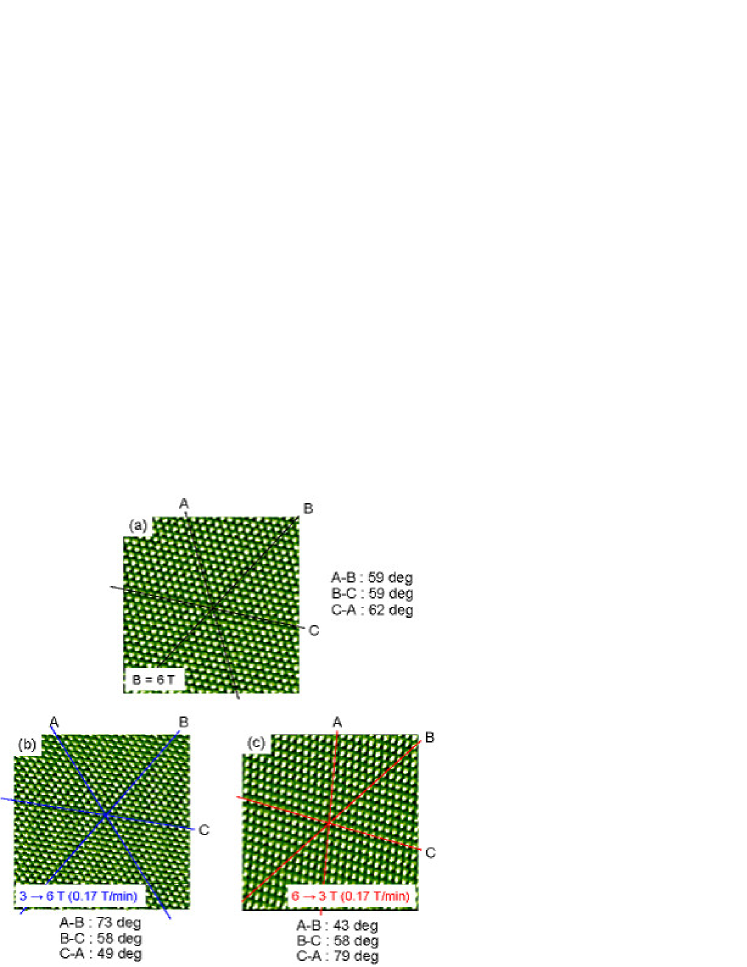
Figure 8(a) is an STM image of a surface of highly oriented pyrolytic graphite (HOPG) obtained at K in T. The image shows a good atomic resolution without any distortions, and this is always true at any stationary fields from 0 to 6 T. What is unusual for this ULT-STM is that similarly clear images are obtained even during sweeping magnetic field from 3 to 6 T and vice versa (Fig. 8(b)(c)). These demonstrate that the system is surprisingly insensitive to the application of magnetic field, which is another distinguished performance of this system. Slight deformations () of the atomic rows are, however, noticed in the images obtained during the field sweep. This is presumably due to a weak magnetic force produced by a tiny magnetization of the STM head.
III.4 Sample preparation in UHV
Taking advantage of the UHV compatibility of this ULT-STM, we made STM imaging and STS measurements on quasi zero-dimensional (0D) and two-dimensional (2D) electron systems in an InAs film. The InAs film (30–100 nm thick) was grown on a GaAs(111)A substrate by the same molecular-beam epitaxy method as that described by Kanisawa et al. kanisawa in a separate UHV chamber. The InAs surface was passivated in situ by evaporation of an As film. Then the sample was transferred to the ULT-STM through an temporary exposure to air. We succeeded in retaining the clean surface after removing the As passivation layer by heating up to 380 ∘C in UHV. Figure 9 shows STM images of an InAs surface obtained in such a way. A stacking-fault tetrahedron, in which the quasi 0D electron system is confined, (Fig. 9(a)) and individual surface In atoms with the reconstructed pattern are clearly visible (Fig. 9(b)). In addition, the Landau quantization of the 2D electron system is observed in TS measurements at temperatures below 30 mK in magnetic fields up to 6 T niimiinas . These measurements became possible only using the present ULT-STM with the full UHV compatibility.
Acknowledgments
This work was financially supported by Grant-in-Aid for Specially Promoted Research (No. 10102003) and Grant-in-Aid for Scientific Research on Priority Areas (Nos. 17071002, 17071007) from MEXT, Japan, Exploratory Research for Advanced Technology Project of JST (Tarucha Mesoscopic Correlation Field Project) and Grant-in-Aid for Young Scientists (A) from JSPS (No. 17684011). We are grateful to Y. Hirayama and K. Kanisawa for supplying us the InAs thin layer samples. We thank I. Ueda and T. Shishido for their technical assistance in the early stage of this work and Unisoku Co., Ltd. for their technical support in designing and assembling the STM head. Encouraging discussions with S. Tarucha and Y. Iye throughout this work were helpful for us. T.M. and Y.N. acknowledge the JSPS Research program for Young Scientists.
References
- (1) S. H. Pan, E. W. Hudson, and J. C. Davis, Rev. Sci. Instrum. 70, 1459 (1999).
- (2) M. Kugler, Ch. Renner, Ø. Fischer, V. Mikheev, and G. Batey, Rev. Sci. Instrum. 71, 1475 (2000).
- (3) J. Wiebe, A. Wachowiak, F. Meier, D. Haude, T. Foster, M. Morgenstern, and R. Wiesendanger, Rev. Sci. Instrum. 75, 4871 (2004).
- (4) H. F. Hess, R. B. Robinson, and J. V. Waszczak, Physica B 169, 422 (1991).
- (5) H. Fukuyama, H. Tan, T. Handa, T. Kumakura, and M. Morishita, Czech. J. Phys. 46, 2847 (1996).
- (6) M. D. Upward, J. W. Janssen, L. Gurevich, A. F. Morpurgo, and L. P. Kouwenhoven, Appl. Phys. A 72, S253 (2001).
- (7) N. Moussy, H. Courtois, and B. Pannetier, Rev. Sci. Instrum. 72, 128 (2001).
- (8) H. Suderow, M. Crespo, P. Martinez-Samper, J. G. Rodrigo, G. Rubio-Bollinger, S. Vieira, N. Luchier, J. P. Brison, and P. C. Canfield, Physica C 369, 106 (2002).
- (9) T. Hanaguri, C. Lupien, Y. Kohsaka, D.-H. Lee, M. Azuma, M. Takano, H. Takagi, and J. C. Davis, Nature 430, 1001 (2004).
- (10) The early design of our ULT-STM was described in T. Matsui, H. Kambara, and H. Fukuyama, J. Low Temp. Phys. 121, 803 (2000).
- (11) A preliminary report of the construction of ULT-STM is given in T. Matsui, H. Kambara, I. Ueda, T. Shishido, Y. Miyatake, and H. Fukuyama, Physica B 329-333, 1653 (2003).
- (12) Y. Niimi, K. Kanisawa, H. Kojima, H. Kambara, Y. Hirayama, S. Tarucha, and H. Fukuyama, (to be published in J. Phys: Conf. Ser.).
- (13) T. Matsui, H. Kambara, Y. Niimi, K. Tagami, M. Tsukada, and H. Fukuyama, Phys. Rev. Lett. 94, 226403 (2005).
- (14) Y. Niimi, T. Matsui, H. Kambara, and H. Fukuyama, Physica E 34, 100 (2006).
- (15) Y. Niimi, H. Kambara, T. Matsui, D. Yoshioka, and H. Fukuyama, Phys. Rev. Lett. 97, 236804 (2006).
- (16) H. Kambara, Y. Niimi, K. Takizawa, H. Yaguchi, Y. Maeno, and H. Fukuyama, AIP Conf. Proc. 850, 539 (2006).
- (17) Model Kelvinox-100, Oxford Instruments. The cooling power is 100 W at 100 mK, and the base temperature without heat load is 9.4 mK.
- (18) converter Model 1211, DL Instruments.
- (19) SCALA PRO 4.1 System, OMICRON NanoTechnology GmbH.
- (20) The STM head was designed and assembled in collaboration with Unisoku Co., Ltd.
- (21) H. Fukuyama, Solid State Phys. 30, 938 (1995) in Japanese.
- (22) Manufactured by Unisoku Co., Ltd.
- (23) H. F. Hess, R. B. Robinson, R. C. Dynes, J. M. Valles, Jr., and J. V. Waszczak, Phys. Rev. Lett. 62, 214 (1989).
- (24) M. Tinkham, Introduction to Superconductivity, (McGraw-Hill, 1996).
- (25) E. L. Wolf, Principles of Electron Tunneling Spectroscopy, (Oxford University Press, 1985).
- (26) J. G. Rodrigo, H. Suderow, and S. Vieira, Euro. J. Phys. B 40, 483 (2004).
- (27) S. H. Pan, E. W. Hudson, and J. C. Davis, Appl. Phys. Lett. 73, 2992 (1998).
- (28) K. Kanisawa, M. J. Butcher, Y. Tokura, H. Yamaguchi, and Y. Hirayama, Phys. Rev. Lett. 87, 196804 (2001).