In-plane optical anisotropy due to conduction band electron wavefunctions
Abstract
Photoluminescence measurements were carried out on Be -doped GaAs/Al0.33Ga0.67As heterostructure at 1.6 K in magnetic fields () up to 5 T. Luminescence originating from recombination of a two-dimensional electron gas (2DEG) and photo excited holes localized on Be acceptors was analyzed. The degree of circular polarization () of the luminescence from fully occupied Landau levels was determined as a function of and the 2DEG concentration, . At constant, decreased with the increase of . Two mechanisms of the dependence are discussed: a) the Stark effect on a photo excited hole bound to Be acceptor and b) the in-plane anisotropy of the intensity of optical transitions. A quantitative analysis shows that the influence of the Stark effect on is negligible in the present experiment. We propose that the dependence results from the symmetry of conduction band electron wavefunctions and we give qualitative arguments supporting this interpretation.
pacs:
71.70.Ej, 78.67.DeI Introduction
Let us consider a GaAs/AlGaAs heterostructure. The point symmetry group of the constituent semiconductors is , but the presence of the interface reduces the symmetry of the heterostructure to . Lowering the symmetry has important consequences on optical properties, leading to an anisotropy in the (001) plane. This anisotropy is of the current interest and is studied both experimentally and theoretically. The landmark experiments were carried out by Jusserand et al. Jusserand1 ; Jusserand2 , Kwok et al. Kwok , Krebs and Voisin Krebs , and Kudelski et al. Kudelski . These measurements were accompanied by theoretical considerations concentrating on the anisotropic spin splitting of the conduction band Andrada ; Pfeffer , the anisotropy of the Raman scattering Froltsov and the anisotropy due to the heavy hole - light hole mixing by the interface potential Ivchenko2 . A comprehensive review of experimental data and theoretical models developed to investigate the anisotropy of heterostructures and quantum wells can be found in Winkler .
In the present paper we consider an influence of the symmetry lowering on the degree of circular polarization of the luminescence originating from a single GaAs/AlGaAs heterostructure. The investigated heterstructure was grown in the [001] direction. A high mobility quasi two dimensional electron gas (2DEG) is located at the interface due to Si donor doping of the barrier. A diluted sheet of Be acceptors is introduced into the GaAs layer at = 30 nm from the interface. The photoluminescence analyzed originated from transitions between the 2DEG and photo excited holes bound to Be acceptors. Application of the magnetic field () perpendicular to the (001) plane splits the electron and hole levels which leads to a nonzero degree of circular polarization at and at sufficiently low temperatures.
A near-band luminescence observed in 2D structures grown from zinc blende materials is often interpreted as a transition, where (conduction band) and (valence band) are representations of the symmetry group of the bulk crystal at zero wavevector . The corresponding optical selection rules are shown in figure 1a. In such a case, the degree of circular polarization of the luminescence, , is determined only by the magnetic field and the temperature (): the magnetic field determines the value of the Zeeman splitting of the electron and hole levels while the temperature determines their occupation. The selection rules shown in figure 1a are valid for the perfect symmetry of the electron and hole states. A single heterojunction is a structure of the symmetry and the selection rules of figure 1a are relaxed. The resulting scheme (derived further on) is shown in figure 1b. Such a relaxation of the selection rules leads to a decrease of the degree of circular polarization.

The origin of the present paper was an observation of a dependence of on the concentration of the 2DEG () which cannot be explained on the basis of the selection rules shown in figure 1a. To explain the effect observed, we discuss two mechanisms which are related to the heterostructure electric field and lead to selection rules shown in figure 1b. The first one is the Stark effect on a photo excited hole bound to Be acceptor. The second mechanism is an in-plane anisotropy of optical transitions induced by a low symmetry of the heterostructure potential.
The paper is organized as the following. To introduce the idea of the present experiment, we start, in Section 2, with a description of basic facts concerning polarization of the luminescence in acceptor -doped heterostructures. We follow, in Section 3 and Section 4, with the experimental part describing the sample investigated, the experimental set-up and results. Next, in Section 5, we introduce a model of the Stark effect on the hole. Application of the model to the experimental data leads to the conclusion that the Stark effect cannot be responsible for the dependence observed. Then, in Section 6, we propose that it results from a low symmetry of the heterojunction electrostatic potential. We argue that the anisotropy appears due to conduction band electron wavefunctions, and not wavefunctions of holes taking part in the optical transition. Within a phenomenological model we derive appropriate selection rules shown in figure 1b. Finally, we summarize and conclude the paper.
II Polarized luminescence from acceptor -doped heterostructures
Heterostructures similar to that investigated in the present work were already studied by other groups KukushkinAdvances . We recall here some basic facts that are relevant to understand the present experiments and results.
In acceptor -doped heterostructures, acceptors are introduced into the GaAs channel some tens of nanometers from the GaAs/AlGaAs interface. A 2DEG is created in a heterostructure quantum well due to doping of the AlGaAs barrier with shallow Si donors. The photoluminescence (PL) is excited by a laser beam and some of photo excited holes are captured by acceptors in the -layer. A typical luminescence spectrum shows a number of lines corresponding to different transitions, like donor - acceptor or exciton ones. Here we focus only on the radiative recombination of 2D electrons with holes bound to acceptors in the -layer. Since this is the only optical transition analyzed in this paper, the notion "hole" will always have the meaning of a hole bound to an ionized acceptor in the -layer.
If the magnetic field is applied perpendicular to the 2DEG plane, the electron density of states is quantized into Landau levels (LLs) and the degeneracy of the hole ground state is totally removed. In such a case, the PL arising from the recombination of 2D electrons with holes is polarized. The degree of circular polarization , where and are intensities of the and components of the luminescence, respectively. There are two factors that contribute to : polarization of the 2DEG and polarization of the holes. Let us consider an even electron filling factor when the electron gas is composed of an equal number of electrons with the spin up and spin down. Then, is determined by the polarization of holes only, since the electron gas is unpolarized. This is the case considered in the present paper: the polarization of the luminescence observed is caused by a thermal distribution of holes on acceptor levels split by the magnetic field.
Tuning the 2DEG concentration can be achieved by the electrical polarization of a semi-transparent electrode prepared on the sample surface. We use this possibility to perform luminescence measurements as a function of and , and we show that depends on when and are constant.
III Experiment
The sample under investigation was a high quality GaAs/Al0.33Ga0.67As heterostructure grown on semi-insulating GaAs substrate. The GaAs channel of about 1 m above a 50 periods of 5 nm/5 nm GaAs/AlAs superlattice contains unintentional acceptors at a concentration less than 1014 cm-3. The AlGaAs barrier comprises an undoped 45 nm thick AlGaAs spacer and a uniformly Si-doped 35 nm thick AlGaAs layer; the doping level amounts to 1018 cm-3. The -layer of Be atoms with the concentration of 109 cm-2 was introduced into the GaAs channel at the distance = 30 nm away from the GaAs/AlGaAs interface. The barrier was covered with a 15 nm thick GaAs cap layer.
The measurements were carried out in an optical helium cryostat supplied with a 5 T split-coil. All measurements were carried out at 1.6 K and the temperature was stabilized within 0.02 K by pumping the helium gas through a manostat. The luminescence was excited by a He-Ne laser. All data presented in this paper were obtained at the same laser excitation power. Both cw and time-resolved measurements were performed. The power of excitation was a few mW/cm2 and was a few orders of magnitude smaller than that corresponding to a saturation of the luminescence signal. In the case of time - resolved measurements, laser pulses were generated by passing the laser beam through an acoustooptical modulator driven by a generator of rectangular voltage pulses. The time resolution was 5 ns. The luminescence passed through a plate followed by a quartz linear polarizer. The circular polarizations were separated by turning the plate. The luminescence was analyzed by a spectrometer supplied with a CCD camera (for cw measurements) or with a photomultiplier (for time-resolved measurements). In the latter case, the photomultiplier signal was amplified and directed to a photon counter.
A semi-transparent Au gate electrode and an ohmic contact were fabricated on the sample surface and the concentration of the 2DEG was tuned by polarizing the gate in the backward direction. was estimated by determination the magnetic field, , at which the luminescence from the =1 LLs disappears (two Landau levels correspond to each ). Then , where is the electron charge and is the Planck constant.
IV Results
An example of the magnetic field evolution of the luminescence spectrum is shown in figure 2a. With an increase of , the number of populated LLs of the first electrical subband decreases as their degeneracy grows.

The analysis of the polarization of the luminescence starts with a deconvolution of each spectrum into separate Lorentzian peaks corresponding to pairs of LLs (figure 2b). We subtract from the total spectrum Lorentzians corresponding to the second electrical subband and the highest in energy pair of LLs of the first electrical subband ( and peaks in figure 2b). This leaves that part of the spectrum which corresponds to an equal number of LLs occupied with spin-up and spin-down electrons, i.e., to the totally unpolarized electron gas. The area of that part of the spectrum is proportional to the intensity of the luminescence, and used to calculate . This procedure allows to determine at given for different . The results are shown in figure 3. Clearly, depends on , and to interpret this result is the purpose of the present paper.

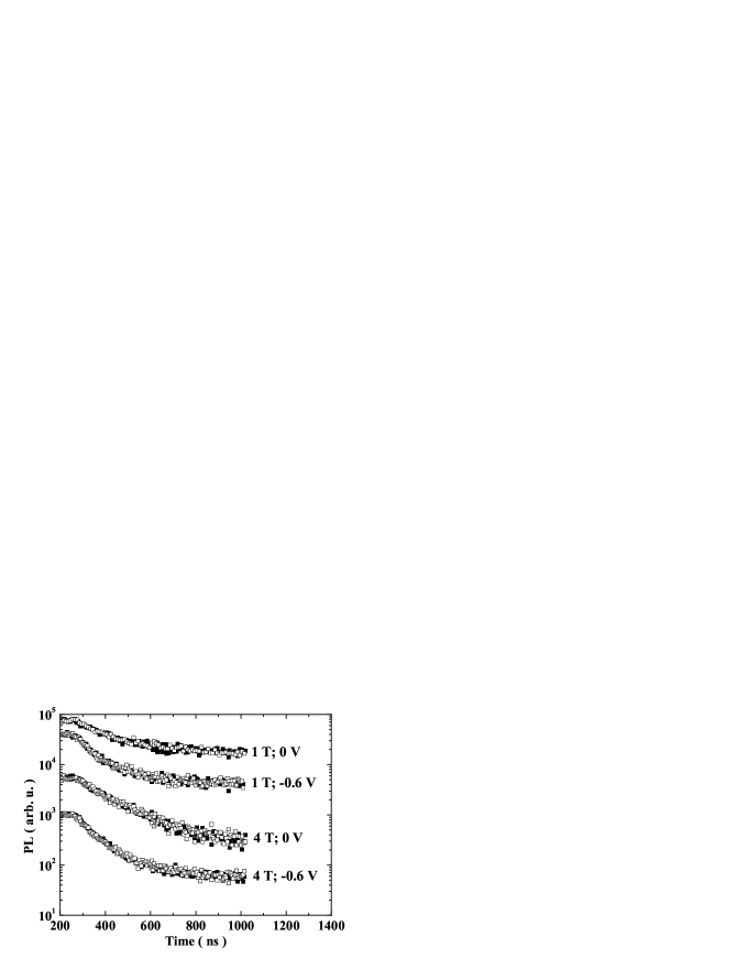
Figure 4 shows examples of a temporal evolution of the luminescence signals measured in (open squares) and (solid squares) polarizations. The data was multiplied by a constant factor to coincide with the data. Corresponding and signals are proportional in the whole time domain, both within the laser pulse, and after the pulse end. The degree of polarization does not depend on time (within the time resolution of the present experiment) which indicates that the system is stationary and time-resolved polarization measurements give the same value of as cw measurements. We used this fact to analyze polarization data obtained from cw measurements which essentially improved the signal to noise ratio.
The fact that the system investigated is stationary does not mean that the distribution of holes on acceptor levels correspond to the temperature of the helium bath surrounding the sample. We refer here to time-resolved polarization studies on similar structures Filin which show that at 1.6 K the relaxation time of photoexcited holes on the acceptor levels is of the order of s. This is a few orders of magnitude shorter than the luminescence decay time which is of the order of s, as can be concluded from figure 4. For this reason, we can assume that photoexcited holes are distributed on the acceptor levels according to an equilibrium thermal distribution corresponding to the helium bath temperature of 1.6 K.
The problem of distribution of electrons is avoided in the present considerations because we take into account the luminescence originating from fully occupied Landau levels only.
V Stark effect on a bound hole
To interpret dependence shown in figure 3, we begin with an analysis of the Stark effect on the acceptor bound hole. This problem was recently considered by Smit et al. Smit who calculated the energy of acceptor levels in the electric field. Our approach is complementary: we take into account the magnetic field, not considered in Smit , and we discuss an influence of mixing of hole levels by the electric field on .
A group theory based Hamiltonian for the hole in the electric () and magnetic field ()was introduced by Bir, Butikov and Pikus BirButikovPikus1 ; BirButikovPikus2 . In the case of both and in the direction, one gets the following perturbation Hamiltonian of the linear Zeeman and linear Stark effects:
| (1) |
where is the Bohr magneton, and are isotropic and anisotropic -factors, respectively, are the = 3/2 orbital momentum matrices, and is the dipole moment of Be acceptor.
Let us denote the unperturbed acceptor wavefunctions as , , where is an envelope function. We choose the following basis of the wavefunctions : (corresponding to the magnetic quantum number = 3/2, 1/2, - 1/2 and -3/2, respectively). and are spin up and down spinors, and , and are functions transforming like , and under operations of the symmetry group, respectively Bhattacharjee . The above Hamiltonian takes the form:
| (2) |
where , describe the linear Zeeman effect and describes the linear Stark effect.
The Hamiltonian given by equation 2 can be diagonalized analytically and explicit formulae for mixed wave functions () are: and , where is a normalizing constant and describes mixing of the wave functions; , where . The corresponding energies are: and . The conduction band states are not affected by the electric field Smit .

In the presence of the electric field, the selection rules shown in figure 1a, valid for , are replaced by the scheme shown in figure 1b which is a result of mixing of with and with states described by the above Hamiltonian. In consequence, a decrease of in comparison with the case can be expected. To determine the magnitude of this effect we use the functions to calculate the intensity of the and transitions in the following way.
According to the time-dependent perturbation theory, the intensity of an optical transition between the states and is proportional to , where e is the polarization vector of the electromagnetic wave and p is the electron momentum. In the case of a transition between electrons occupying Landau levels and holes occupying acceptor levels, the intensity observed in the polarization e is equal to
| (3) |
is a polarization independent factor, is the wave function of a conduction band electron with the spin projection equal to or . Statistical weights describe the probability of occupation of each of four acceptor Zeeman : , where is the energy of the lowest lying level, corresponding to . Statistical weights for electron spin levels, , are equal to 1 because we consider equal number of fully occupied Landau levels with spin up and down.
Let and . Then
| (4) |
In considering the Stark effect we assume in this Section that both electron wavefunctions and hole wavefunctions transform according to representations of the symmetry group. Matrix elements in Eq. 4 can be expressed by . This equality results from the assumed symmetry of wavefunctions and the fact that the and directions are equivalent in the symmetry. We get
| (5) | |||
where .
To calculate as a function of using (V) we estimate the heterostructure electric field in the plane where Be acceptors are placed, . The distribution of charges and the electrostatic potential in the heterostructure were calculated by a self-consistent solution of the Schrödinger and Poisson equations. The overall charge neutrality was guarantied by taking into account interface and surface charges, which simulate also the effect of a gate electrode and which are used to control the concentration of the 2DEG in the heterostructure. The results of the calculations are the subband energies and wavefunctions as a function of the total 2DEG concentration . The calculations show that at = 30 nm, where Be acceptors are placed, the electric field is almost insensitive to : it increases from V/m to V/m when increases from cm-2 to cm-2 (see figure 5).
The -factors of holes bound to Be acceptors in bulk GaAs were obtained in a far infrared experiment by Lewis, Wang and Henini Lewis : and . To calculate , the value of the Be acceptor dipole moment, , should be known. Since, apparently, this data is not available in the literature, let us assume that = 1 D (1 D = 3.3 10-30 Cm). This value is higher than the dipole moment of several different acceptors in bulk Si investigated by Köpf and Lassman KopfLassmann , which was found to fall in the range 0.26 D - 0.9 D. Taking D, K and V/m we can estimate the upper limit of the Stark effect energy corresponding to the present experimental conditions. We get 5 eV, which is negligible in comparison with the thermal energy at 1.6 K. It means that the distribution of holes over the Zeeman levels is not changed by the heterostructure electric field. An influence of mixing of hole levels by the electric field on can be investigated by calculation of for different values of . Results for and V/m are shown in the inset to figure 5. The two curves practically coincide: for the magnetic field of interest, for these two values of differs by less than .
An analysis presented in this Section shows that it is not possible to explain the dependence by the Stark effect: neither energy shifts of hole levels nor mixing of levels is strong enough to influence significantly.
VI Circular polarization of luminescence from systems of the symmetry
Let us analyze now the influence of the low symmetry of the heterostructure potential on . In structures of the symmetry, the directions ([10]) and ([110]) are not equivalent which leads to an anisotropy of optical transitions in the (001) plane. This leads to experimentally observed nonzero degree of the linear polarization: . It will be shown below that in systems of the symmetry, and are related to each other:, where is the degree of circular polarization for the symmetry. The increase of the strength of perturbation causing symmetry lowering results in an increase of and a corresponding decrease of . For this reason, effects of the symmetry lowering can be investigated by an analysis of .
A basis for modeling the relation between a low symmetry of a quantum system and its optical anisotropy is a theory of Ivchenko et al. Ivchenko2 . According to this theory, the anisotropy originates from mixing of light and heavy valence band holes while it is explicitly assumed that the symmetry of conduction band electron wavefunctions is preserved. Rösller and Kainz, starting from the theory of Ivchenko et al., showed that the coupling of the valence and conduction bands leads to [110] vs. [10] anisotropy of the conduction band wavefunctions Rossler . These calculations were carried out for the case only.
A special feature makes the heterostructure investigated in this work different from other systems of the symmetry studied by other groups. The point is that holes participating in optical transitions are localized as far as 30 nm from the interface (i.e., about 10 Bohr radii) and the influence of the localized interface potential on the holes can be neglected. We showed that the long-range heterostructure potential is also too weak to mix hole levels significantly. Other mixing mechanisms, like the internal stress or stress-related piezoelectric effects, even if present, do not depend on the electron concentration.
For this reason, we propose that the anisotropy results from a low symmetry of conduction band electron wavefunctions. We propose that the source of the anisotropy is a perturbation of the valence band induced both by the localized interface potential and the long-range heterostructure electric field. These perturbations do not influence holes localized on Be acceptors, as we argued above, but only the valence band states in the region of the GaAs channel where the heterostructure electric field is strong and the density of conduction band electron wavefunction is large. Next, the symmetry of conduction band electron wavefunctions is lowered due to the coupling of bands described in Rossler . The perturbation increases with the electron wavevector which means that it becomes stronger when increases. We propose that the dependence observed results from changes of the heterostructure electric field correlated to changes in the 2DEG concentration.
As in the theory of Ivchenko2 , we point at two factors contributing to the symmetry lowering: the long-range heterostructure electric field (leading to the Pockels effect) and the localized interface potential. In fact, figure 5 shows that for nm a large increase, of the order of 106 V/m, of the heterostructure electric field is observed with the increase of . This means that a perturbation of the valence band, and in consequence, of the conduction band, increases with . Also, when increases, the heterostructure well becomes narrower, electron wavefunctions shift towards the interface and the influence of the localized interface potential on the electron states increases. The latter mechanism should lead to much stronger effects in the case of the single interface in the heterostructure investigated in comparison to quantum wells. The reason is that in quantum wells of the symmetry, contributions of the two interfaces enter with opposite signs and partially cancel each other. Also, the fact that Be-bound holes are unperturbed, makes effects of lowering the symmetry of the conduction band states more evident.
Carrying out calculations similar to these presented in Rossler with taking into account the magnetic field is beyond the scope of the present paper. We propose, however, a phenomenological description of the polarization in the system investigated which allows us to derive selection rules for optical transitions between an electron of the symmetry and a bulk-like hole of the symmetry.
>From Eq. 3 one can calculate the intensity of the transition for the [110] () and [10] () polarizations to get
| (6) |
In the symmetry, the directions [110] and [10] are equivalent ( = 0 in this case) and the above expression is equal to zero. This is possible only when
| (7) |
To get a non zero value of with perturbed electron wavefunctions of the symmetry, it is necessary that
| (8) |
where the first equation reflects the equivalence of the [100] and [010] directions in the symmetry.
Calculation of matrix elements with taking into account (8), gives the selection rules of optical transitions observed in the circular polarizations in the symmetry. Non zero intensities are shown by arrows in figure 1b. Lowering the symmetry of conduction band wavefunctions leads to relaxation of selection rules and a decrease of caused by mixing of and transitions.
To quantify the model, we introduce a real (see below) parameter and we assume that
| (9) |
describes an evolution of matrix elements when the symmetry is lowered. We get
| (10) |
where
| (11) |
The degree of circular polarization is
| (12) |
while . (Assuming that is complex, one can calculate the degree of linear polarization between the [100] and [010] directions: which is equal to zero because these directions are equivalent. This implies .)
Assuming that , where transforms into when the symmetry lowers from to , does not depend on and is equal to - the degree of circular polarization that would be measured in the case when both the electron and hole states were of the symmetry. These allow us to derive the relation between and mentioned above.
To estimate the range of corresponding to measured, we use Eq. 12 which gives , where . With data of figure 3 and , we get results presented in figure 6 showing increasing from about 0.2 to 0.5 with increasing from 1011 cm-2 to cm-2.

The results presented in this Section allow us to suggest that a widely used approximation of conduction band electron wavefunctions as unperturbed functions of the symmetry is not generally valid. The symmetry lowering of conduction band states results from the perturbation of the valence band by a long-range heterostructure electric field and the localized interface potential. Measurements on heterostructures with different barrier height could help to separate these two contributions. This is because the role of the localized interface potential should strongly increase with lowering the barrier height due to an exponential increase of penetration of the barrier by electron wavefunctions.
VII Summary and conclusions
Low temperature polarized magnetoluminescence experiments on a high quality GaAs/AlGaAs heterostructure with Be acceptor -layer incorporated into the GaAs channel were carried out. A metallic gate on the sample surface allowed to tune the 2DEG concentration in the heterostructure. The degree of circular polarization of the luminescence originating from transitions between 2DEG and photoexcited holes bound to Be acceptors was analyzed. We observed that decreases with the increase of . In principle, this effect can be explained by the Stark effect on Be - localized hole and/or by an in-plane anisotropy of optical transitions, reflecting the symmetry of the heterstructure potential. An analysis of the Stark effect was based on a group theory Hamiltonian, with taking into account results of self-consistent calculations of the heterostructure electric field. It was shown that the Stark effect can be neglected in the heterstructure investigated, which led to the conclusion that the effect responsible for the dependence is a low symmetry of the heterostructure potential. We argued that Be-localized holes are of the symmetry which led us to the conclusion that the optical anisotropy is related to a low symmetry of the conduction band electron wavefunctions. We propose that this symmetry lowering results from a perturbation of the valence band which induces perturbation of the conduction band due to the coupling. We used symmetry arguments to derive selection rules of optical transitions in the case when the conduction band electrons and holes are of the and symmetry, respectively, and we provided a phenomenological description of the experimental data.
In conclusion, it is proposed that due to a large separation of holes from the interface, the in-plane anisotropy observed is due to lowering of the symmetry of the conduction band electron wavefunctions only. The mechanism responsible for the symmetry lowering is a perturbation of the valence band states which influences the conduction band states through the coupling. The increase of the perturbation with is caused by an increase of the heterostructure electric field with . Measurements on heterostructures with different barrier heights could help to separate a contribution from the localized interface potential from that of the long-range electric field.
Acknowledgements.
J. Ł. is thankful to M. Grynberg and A. Łusakowski for discussions.References
References
- (1) Jusserand B, Richards D, Peric H and Etienne B 1992 Phys. Rev. Lett. 69 848
- (2) Jusserand B, Richards D, Allan G, Priester C and Etienne B 1995 Phys. Rev. B 51 4707
- (3) Kwok S H, Grahn H T, Ploog K and Merlin R 1992 Phys. Rev. Lett. 69 973
- (4) Krebs O, Rondi D, Gentner J L, Goldstein L and Voisin P 1998 Phys. Rev. Lett. 80 5770
- (5) Kudelski A, Golnik A, Gaj J A, Kyrychenko F V, Karczewski G, Wojtowicz T, Semenov Yu G, Krebs O and Voisin P 2004 Phys. Rev. B 64 045312
- (6) de Andrada e Silva E A Phys. Rev. 1992 B 46 1921
- (7) Pfeffer P 1999 Phys. Rev. B 59 15902
- (8) Froltsov V A, Mal’shukov A G and Chao K A 1999 Phys. Rev. B 60 14255
- (9) Ivchenko E L, Toropov A A and Voisin P 1998 Physics of the Solid State 40 1748
- (10) Winkler R 2003 Spin-Orbit Coupling Effects in Two-Dimensional Electron and Hole Systems (Springer Tracts in Modern Physics vol 191) (Berlin: Springer)
- (11) Kukushkin I V and Timofeev V B 1996 Advances in Physics 45 147
- (12) Filin A I, Dite A F, Kukushkin I V, Volkov O V and von Klitzing K 1992 JETP-Letters 56 156
- (13) Smit G D J, Rogge S, Caro J and Klapwijk T M 2004 Phys. Rev. B 70 035206
- (14) Bir G L, Butikov E I and Pikus G E 1963 J. Phys. Chem. Solids 24 1467
- (15) Bir G L, Butikov E I and Pikus G E 1963 J. Phys. Chem. Solids 24 1475
- (16) Bhattacharjee A and Rodriguez S 1972 Phys. Rev. B 6 3836
- (17) Lewis R A, Wang Y J and Henini M Phys. Rev. 2003 B 67 235204
- (18) Köpf A and Lassmann K Phys. Rev. Lett. 1992 69 1580
- (19) Kohn W 1957 Solid State Physics ed F Seitz and D Turnbull (New York: Academic) vol 5 p 257
- (20) Rössler U and Kainz J 2002 Solid State Commun. 121 313