External field control of donor electron exchange at the Si/SiO2 interface
Abstract
We analyze several important issues for the single- and two-qubit operations in Si quantum computer architectures involving P donors close to a SiO2 interface. For a single donor, we investigate the donor-bound electron manipulation (i.e. 1-qubit operation) between the donor and the interface by electric and magnetic fields. We establish conditions to keep a donor-bound state at the interface in the absence of local surface gates, and estimate the maximum planar density of donors allowed to avoid the formation of a 2-dimensional electron gas at the interface. We also calculate the times involved in single electron shuttling between the donor and the interface. For a donor pair, we find that under certain conditions the exchange coupling (i.e. 2-qubit operation) between the respective electron pair at the interface may be of the same order of magnitude as the coupling in GaAs-based two-electron double quantum dots where coherent spin manipulation and control has been recently demonstrated (for example for donors nm below the interface and nm apart, meV), opening the perspective for similar experiments to be performed in Si.
pacs:
03.67.Lx, 85.30.-z, 73.20.Hb, 85.35.Gv, 71.55.CnI Introduction
Doped Si is a promising candidate for quantum computing Kane (1998) due to its scalability properties, long spin coherence times, de Sousa and Das Sarma (2003); Tyryshkin et al. (2003); Abe et al. (2004); Witzel et al. (2005); Tyryshkin et al. (2006); Witzel and Das Sarma (2006) and the astonishing progress on Si technology and miniaturization in the last few decades (Moore’s law). The experimental production of a working qubit depends on precise positioning (of the order of Å) Koiller et al. (2002a); Kane (2005) of donors in Si and the quantum control of the donor electrons by local gates placed over an oxide layer above the donors. The required accuracy in donor positioning has not been yet achieved, although there are increasing efforts in this direction, using top-down techniques, i.e. single ion implantation (with tens of nm accuracy), Schenkel et al. (2003); Shinada et al. (2005); Jamieson et al. (2005) and bottom up techniques, i.e. positioning of P donors on a mono-hydride surface via STM (with nm accuracy) with subsequent Si overgrowth. O’Brien et al. (2001); Schofield et al. (2003)
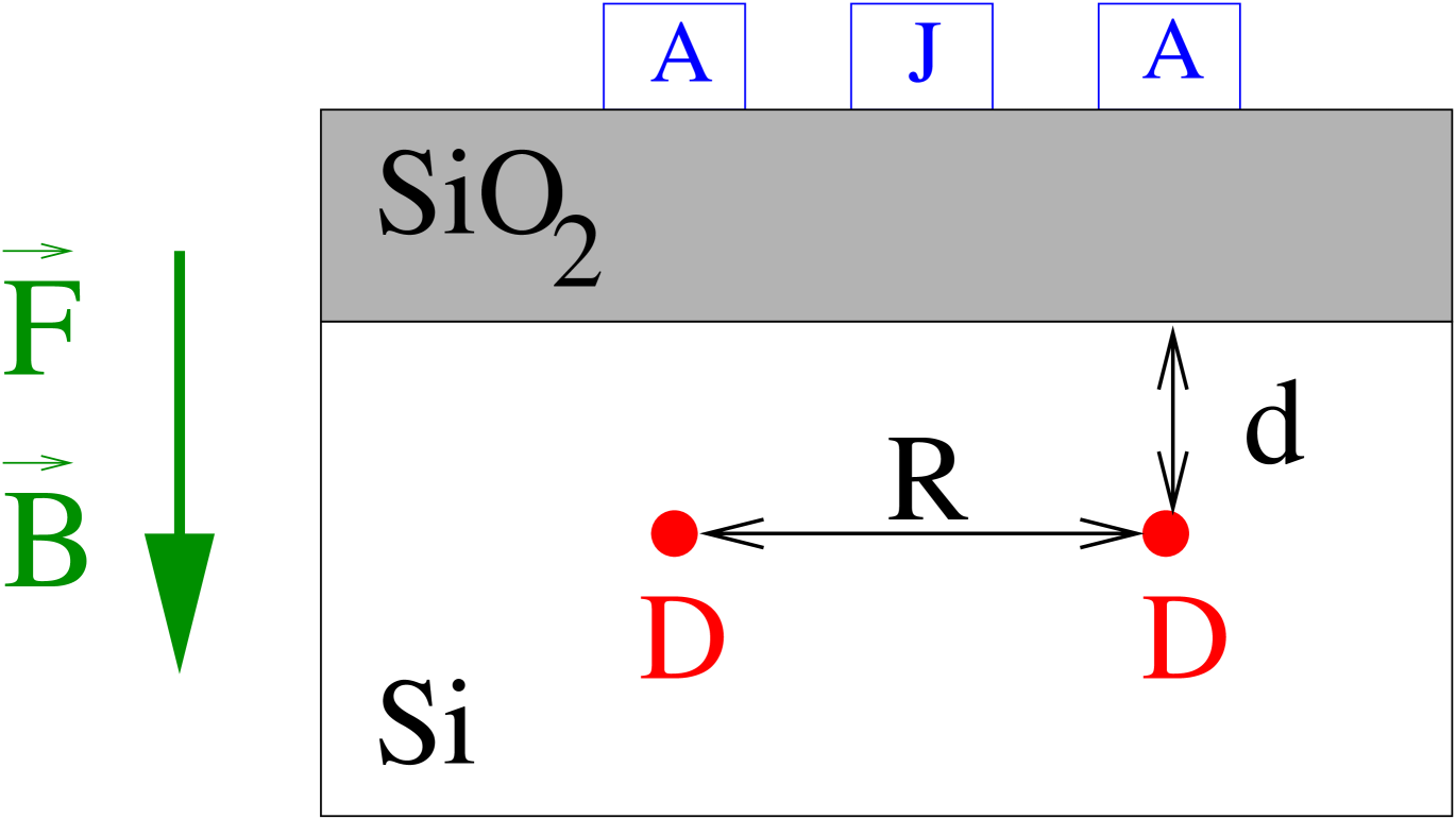
In the original doped Si based quantum computer proposal, Kane (1998) illustrated in Fig. 1, the qubits are the donor nuclear spins, and the hyperfine interaction between these and the donor electron spins is used to perform single qubit operations (rotations). The strength of the hyperfine interaction is manipulated by local surface gates, the so called A-gates, which move the electron between the donor and an interface with SiO2. Exchange between neighboring donors, tuned by surface ’exchange’ gates (J-gates), would control two-qubit operations. Exchange gates were originally proposed for a double quantum dot geometry in GaAs. Loss and DiVincenzo (1998) Related proposals in Si use the electron spin as qubit Vrijen et al. (2000); Levy (2001); Friesen et al. (2003) or the electron charge. Hollenberg et al. (2004a) Charge coherence in Si is much shorter ( ns) Gorman et al. (2005) than the spin coherence ms, which can be further enhanced by isotopic purification, de Sousa and Das Sarma (2003); Witzel et al. (2005); Tyryshkin et al. (2006) making spin qubits in general more attractive than charge qubits for actual implementations. On the other hand, direct detection of a single spin is a very difficult task, Rugar et al. (2004); Xiao et al. (2004); Koppens et al. (2006) while a fraction of a single electron charge can be easily detected with state-of-the-art single electron tunneling (SET) devices. As a result, ingenious spin-to-charge conversion mechanisms, that would allow the electron spin state to be inferred according to the absence or presence of charge detected by an SET at the surface, have been proposed, e.g. Refs. Hollenberg et al., 2004b; Greentree et al., 2005; Stegner et al., 2006; Calderón et al., 2006a.
Doped Si has two main advantages over GaAs quantum dots: (i) The much longer spin coherence times, that can be enhanced by isotopic purification (note that all isotopes of Ga and As have nuclear spins so the spin coherence time in GaAs cannot be improved via isotopic purification), and (ii) the identical Coulomb potentials created by donors as opposed to variable quantum dot well shapes produced by surface gates on a 2-dimensional electron gas (2DEG). Despite this latent superiority of Si, progress in GaAs has been much faster, Petta et al. (2005); Koppens et al. (2005); Johnson et al. (2005); Koppens et al. (2006); Laird et al. (2006) in particular due to the fact that the electrons, being at the device surface, are easier to manipulate and detect. Another Si handicap is that the exchange between donors in bulk Si oscillates, changing by orders of magnitude when the relative position of neighboring donors changes by small distances Å. Koiller et al. (2002a, b) This is caused by interference effects between the six degenerate minima in the Si conduction band. However, as discussed below, this degeneracy is partially lifted at the interface, thus the oscillatory behavior may not represent such a severe limitation for interface states as compared to the donor bulk states.
In the following, we analyze the manipulation of donor electrons close to a Si/SiO2 interface by means of external uniform electric and magnetic fields. Calderón et al. (2006b, c) In Sec. II we introduce the model for an isolated donor and discuss the interface and the donor ground states, which are calculated variationally. We also analyze the shuttling between the interface and the donor, including the effect of a magnetic field. In Sec. III we study the conditions to avoid the formation of a 2DEG at the interface, and discuss the advantages and actual feasibility of performing two-qubit operations at the interface. A summary and conclusions are given in Sec. IV.
II Single donor
II.1 Model
We consider initially a single donor a distance from a Si/SiO2 (001) interface. As a simple model for the A-gate effects, a uniform electric field is applied in the -direction, as illustrated in Fig. 1. The inter-donor distance is assumed to be large enough so that each donor can be treated as an isolated system. The conduction band of Si has six equivalent minima located along the lines. As discussed below, it is reasonable to treat this system within the single-valley effective mass approximationKohn (1957); Stern and Howard (1967); Martin and Wallis (1978); MacMillen and Landman (1984); Ando et al. (1982) leading to the following Hamiltonian for the donor electron
| (1) |
We also consider an applied magnetic field along : In this case the vector potential is included in the kinetic energy term, . The effective masses in Si are , and . The second term is the electric field linear potential, the third is the donor Coulomb potential, and the last two terms (with ) take account of the charge images of the donor and the electron, respectively. , where and . In this case and, therefore, the images have the same sign as the originating charges. In rescaled atomic units, nm and meV, and the Hamiltonian is written
| (2) | |||||
where , with the magnetic length, cm/kV, and the electric field is given in kV/cm.
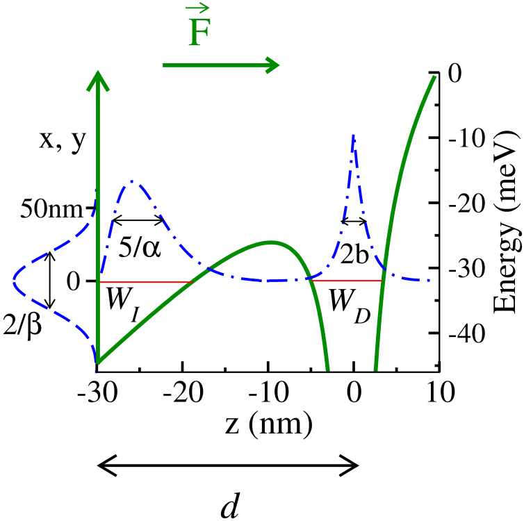
The system under study consists of a shallow donor, P in particular, immersed in Si a distance from a SiO2 barrier, which we assume to be infinite (impenetrable). When no external field is present, the electron is bound to the donor potential well . When an electric field is applied in the -direction, a triangular well is formed next to the interface. The interface well also includes the donor and its image Coulomb potentials at the interface () which, under special circumstances discussed below, are strong enough to localize the electron in the -plane. The interface well and the donor Coulomb potential form an asymmetric double well, as illustrated in Fig. 2.
The Hamiltonian in Eq. (2) is solved in the basis formed by and , which are the ground eigenstates of each of the decoupled wells and . The Hamiltonian is written
| (3) |
where the last term is added to avoid double counting of the impurity Coulomb potential at the interface included both in and , which are defined as
| (4) |
and
| (5) |
The first term in Eq. (4) is the sum of the donor Coulomb potential and its image charge potential at the interface.
The Hamiltonian in the non-orthogonal basis reads
| (6) |
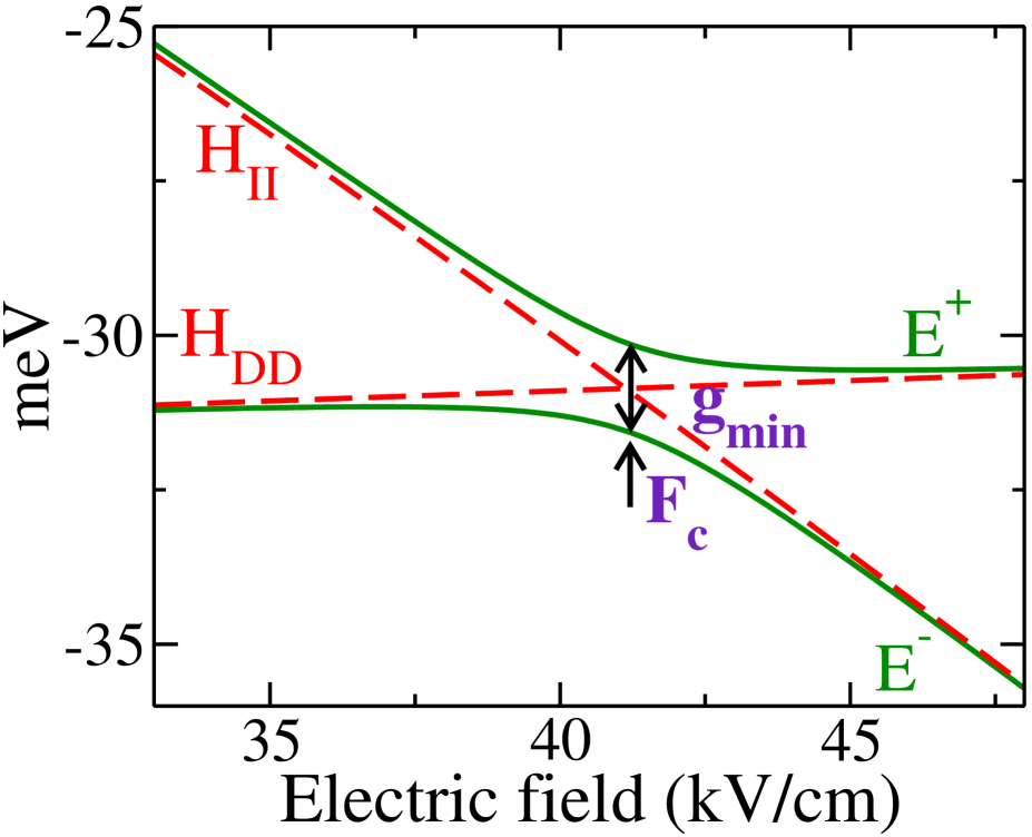
where with . Diagonalization gives the two eigenstates and with eigenenergies and which show anticrossing behavior with a minimum gap when . This point defines the characteristic field , illustrated in Fig. 2, which is relevant for the tunneling process discussed in detail in Sec. II.4.
II.2 Interface state
It is convenient to write the interface potential as a sum of purely - and purely -dependent terms:
| (7) | |||||
| (8) | |||||
| (9) |
The component is the triangular well plus the electron image charge potential, while the component is the sum of the impurity and its image potential at the interface. is plotted in Fig. 3(a) for three different values of . Curves corresponding to the parabolic approximation of the potential,
| (10) |
are also shown, and it is clear that the harmonic approximation works better for the larger distances . Electron confinement at the interface -plane is provided by , while the uniform electric field and the oxide confine the electron along the -direction. For certain values of and , is deep enough to localize the individual donor electrons (with no need of local A-gates) and keep them from forming a 2DEG at the interface: The necessary conditions are discussed in Sec. III.1. The spacial localization of the electrons at the interface is a necessary condition for Si-based quantum computing if qubit read-out takes place at the interface. Kane (1998)
The ground state at the interface is calculated by solving variationally with a separable trial function
| (11) |
For the -part we use
| (12) |
for . The infinite barrier at the interface is taken into account by forcing the ground state to be zero at the interface, so for . is a variational parameter that minimizes the contribution to the energy . The most suitable value for is chosen by comparing and with the exact solution of an infinite triangular well Stern (1972)
| (13) |
where is the Airy function, , and is the ground state energy
| (14) |
The results are shown in Fig. 4 for , , and . gives the best agreement with the exact solution for both the energy and the wave-function and is therefore adopted in what follows.
For the -part we use the ansatz
| (15) |
with the variational parameter calculated by minimizing . We have checked that this gaussian form gives lower energy than an exponential (as a reminiscent of the donor wave-function) for distances nm.
In Fig. 3(b) we plot the energy for the ground state and the first excited state () for both the variational solution adopted here and the parabolic approximation of . The parabolic approximation gives an underestimation of the binding energies and diverges at short distances (not shown). To guarantee that the electron remains bound, and at the ground state, the operating temperature has to be lower than the energy difference between the ground and the first excited states . For nm, the excitation gap meV. This limits the operating temperature to a few Kelvin (in current experiments, temperatures as low as K are being used). Ferguson et al. (2006); Brown et al. (2006)
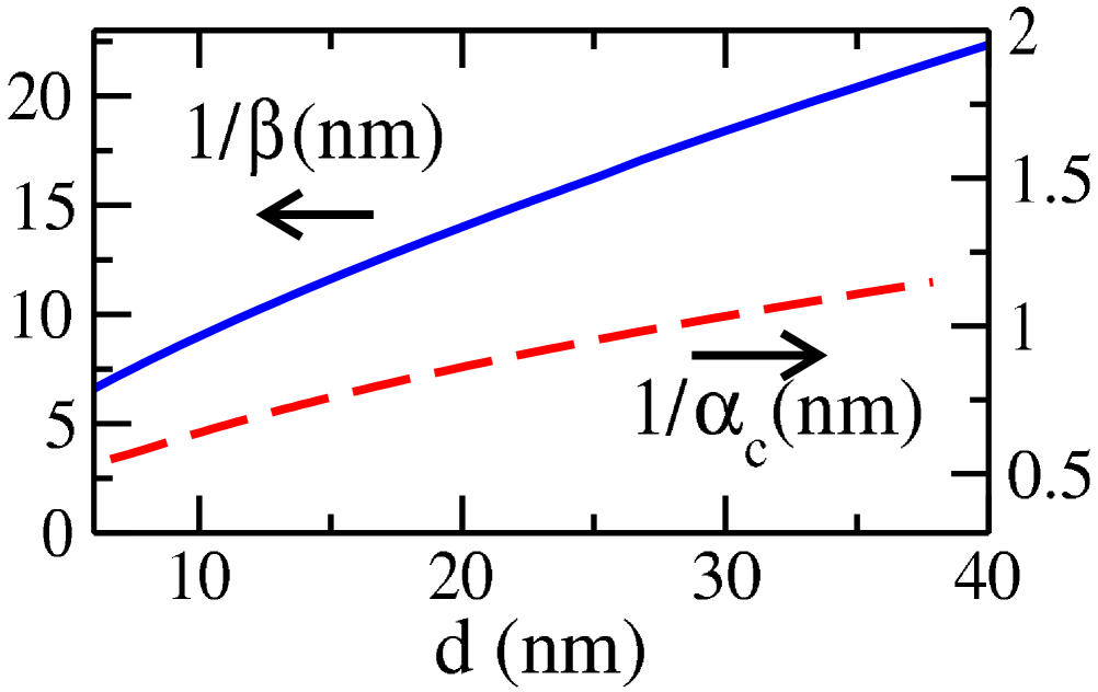
The inverse of the variational parameters, and , are proportional to the confinement lengths in the -direction and the -plane respectively. Both depend on the distance of the donor from the interface as shown in Fig. 5, and also depends on the value of the applied electric field, being larger for smaller . Fig. 5 gives the value of for the electric field at which the expectation values of the energies of the states at the interface and at the donor are degenerate. The expectation value of the position of the electron in the -direction is from the interface. This value is small compared to (for nm, nm), justifying the validity of the two-well approach we are using to solve the Hamiltonian.
At the interface, the -valleys’ energy is lower than the -valleys’. This is straightforward to show for an infinite triangular potential Stern (1972) in which [see Eq. (14)] . The difference between the levels depends on the electric field as . is shown in Fig. 7 (a) (right axis). For a field kV/cm, which is small for our interests, the splitting is meV which corresponds to K. If a magnetic field is applied, the -levels increase their energy faster than the -levels until they cross. However, this crossing happens at a very large magnetic field T (shown in the left axis of Fig. 7 (a) as a function of the electric field ). Therefore, for the range of parameters of interest here, the -valleys are always the ground state at the interface. We point out that it is experimentally established that, in MOSFET geometries equivalent to the one studied here, the interface ground state is non-degenerate, with a 0.1 meV gap from the first excited state.Ando et al. (1982) This is well above the operation temperatures in the quantum control experiments investigated in the present context.
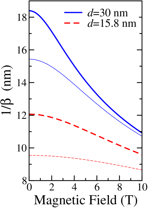
The magnetic field has two main effects on the states: (i) the electron gets more confined in the direction parallel to the interface and, consequently, (ii) its kinetic energy increases. The effect of the magnetic field is strongest for the less confined wave-functions, which correspond to the larger ’s. We can quantify the strength of this effect by calculating the magnetic field that is needed to get a magnetic length of the same order of the confinement length in the plane parallel to the interface: for a donor a distance nm, nm and T while for nm, nm and T. The confinement effect is illustrated in Fig. 6 where as a function of magnetic field for two different values of is shown. The thick lines correspond to the variational solution of minimizing
| (16) |
with trial function . Closer donors produce a larger confinement of the interface electron wave-function but the effect of the magnetic field is much more dramatic for the donors further away from the interface: for nm, a magnetic field of T decreases the wave-function radius by a . Within the parabolic approximation for the interface potential (which overestimates the wave-function confinement) the dependence of on the field is given by Jacak et al. (1998)
| (17) |
with values as shown in Fig. 6 (thin lines).
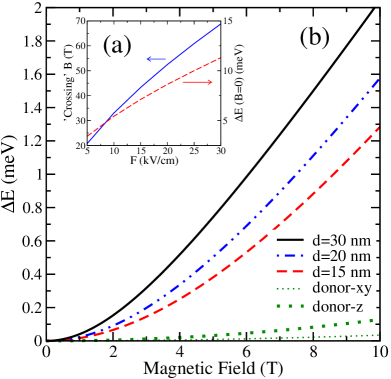
The increase in energy with magnetic field, as calculated variationally, is shown in Fig. 7 (b). We observe again that the effect of the magnetic field is much stronger for the larger values of . The much smaller shift in the donor ground state energy (discussed in the next subsection) is also shown for comparison.
II.3 Donor state
The potential consists of the isolated impurity Coulomb potential
| (18) |
The solution of is taken to be of the form of the anisotropic envelope wave-function, Kohn (1957) multiplied by to satisfy the boundary condition at the interface
| (19) |
where , for . for . For , reduces to the bulk limit . and are variational parameters chosen to minimize the ground state energy. Except for the smallest distances nm, not relevant here, and coincide with the Kohn-Luttinger variational Bohr radii of the isolated impurity () nm and nm.
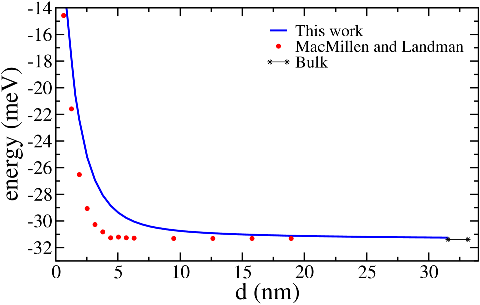
In Fig. 8 we show the variational results for the ground state energy obtained from our trial function . For comparison, we also give results obtained through the trial function proposed by MacMillen and Landman,MacMillen and Landman (1984) where, aiming at a good description for donors at very short distances from the interface (typically smaller than the effective Bohr radius ), a much larger set of variational states was used for the expansion of the donor state. For this comparison, our results in Fig. 8 correspond to a “perfectly imaging” plane (), as assumed in Ref. MacMillen and Landman, 1984. The energy depends strongly on for the smaller values of , and tends to the bulk value at long distances. For the intermediate and large values of of interest here, the two approaches are essentially equivalent.
We find that the effect of the external fields on the donor state is negligible. For instance, for the largest electric fields of interest here ( at short distances nm), the energy corresponding to the electric field potential is , to compare with for the isolated donor ground state in bulk. The effect of a magnetic field on the electron wave-function at the donor is also very small: the field required to get a magnetic length of the order of the Bohr radius nm is T! The donor ground state energy shift due to the magnetic field can be estimated byLandau and Lifshitz (1977)
| (20) |
where lengths are given in units of , for the -envelopes, and for the -envelopes. The results are shown in Fig. 7(b) and are comparable to the values for the 1s orbital of shallow donors calculated numerically in Ref. Thilderkvist et al., 1994. Note that the magnetic field partially breaks the six-valley degeneracy due to the different confinement radius of the electron wave-function in each of the different valleys.
II.4 Shuttling between interface and donor states
We model the donor electron ionization under an applied electric field along by considering the tunneling process from the donor well into the triangular well at the Si/SiO2 interface (see Fig. 2). The required value of the field for ionization to take place may be estimated from [see Eq. (6)]. We call the characteristic field for which this condition is fulfilled, which is equivalent to require that the gap between the two eigenenergies and of is minimum, as illustrated in Fig. 9.
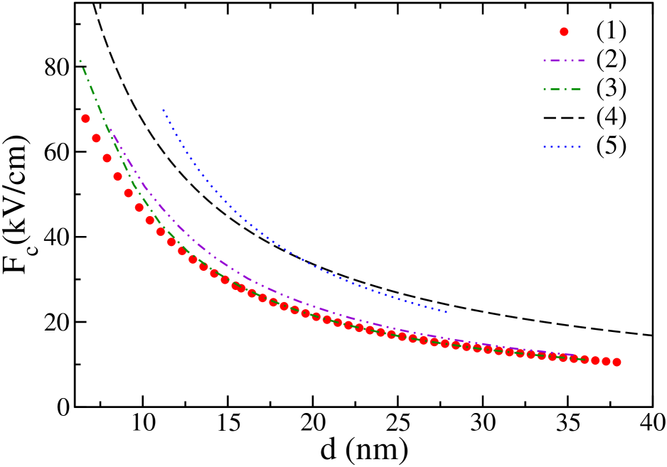
Our results for versus are shown by the solid dots [labelled (1)] in Fig. 10. In this figure we also test the robustness of our approach, namely using as given in Eq. (19), by comparing the values of obtained assuming different forms for the donor trial function. Curves (2) and (3) correspond to isotropic and anisotropic wave-functions respectively, with the same ground state energy for the electron at the donor as obtained from in Eq. (19), meV. Note that they compare very well with curve (1). Curve (4) corresponds to a tight-binding result Martins et al. (2004) in which the six-valley degeneracy of Si is incorporated. Although all curves are qualitatively similar, curve (4) is shifted towards larger fields. The origin of this shift is investigated by considering an isotropic trial function whose parameters have been chosen to give a ground state energy meV, and we note that the results, given in curve (5), compare very well with those in curve (4). We conclude that the shift in the value of when the six-fold degeneracy of the Si conduction band is considered is mainly due to the fact that the ground state energy at the donor in the single valley approximation [curve (1)] is meV while it is meV when the intervalley coupling is included [curve (4)]. In the following we use as defined in Eq. (19), keeping in mind that electric field values are bound to be somewhat underestimated.
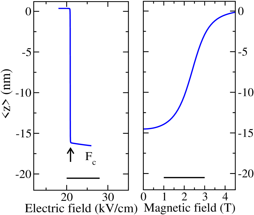
We may picture the electron shuttling between the two wells under applied electric and magnetic fields by calculating the expectation value of its position along at the ground state, . The results for nm are shown in Fig. 11 , where the horizontal lines mark the position of the interface. The distance between and the interface tends to for , where also depends on . In Fig. 11(a) we show pictorially how the electron would evolve from the donor to the interface well when an electric field is applied. At small values of the electron is at the donor well, and . The center of mass is slightly shifted from the donor site due to the factor in . Above , the electron eventually tunnels to the interface. Starting with the electron at the interface in a near-degeneracy configuration (), a relatively modest magnetic field can cause the electron to move in a direction parallel to the field and against the electric field, as shown in Fig. 11(b). This is due to the much larger shift of the interface state energy with magnetic field compared to the shift of the donor ground state energy [see Fig. 7(b)]. This behavior characterizes electrons originating from the donors, and not other charges that the SET may detect, like charges in metallic grains on the device surface. Brown et al. (2006) The combination of parallel electric and magnetic fields constitutes therefore a valuable experimental setup to investigate whether charge detected at the interface actually originates from a donor. Calderón et al. (2006c)
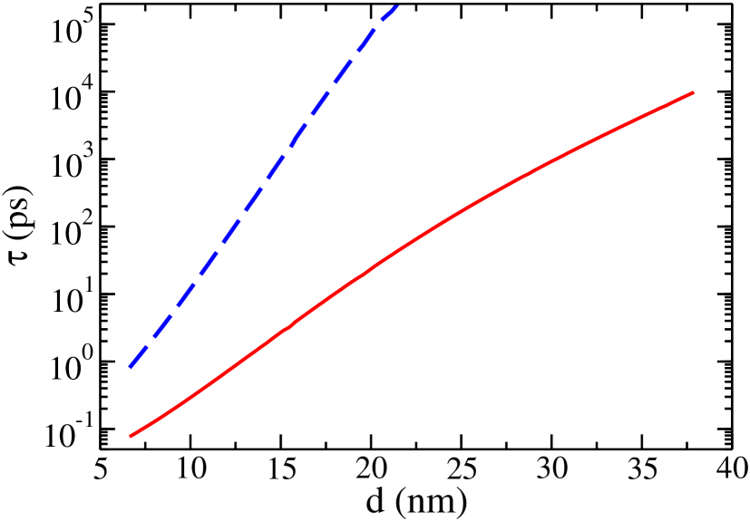
A key parameter determining the feasibility of quantum computation in the doped Si architecture is the time required to shuttle the electron between the donor and the interface. This time should be orders of magnitude smaller than the coherence time to allow for many operations and error correction while coherent evolution of the qubit takes place. The tunneling process conserves the spin, but coherence would be lost for orbital/charge degrees of freedom. Therefore, if quantum information is stored in a charge qubit, the electron should evolve adiabatically from the donor to the interface, while tunneling would be acceptable for spin qubits. In an adiabatic process the modification of the Hamiltonian (for instance, when an external field is applied) is slow enough that the system is always in a known energy eigenstate, going continuously from the initial to the final eigenstate. Messiah (1962) Here, we calculate both tunneling and the adiabatic passage times.
We estimate the tunneling time from the minimum gap between the two eigenvalues and (see Fig. 9) via the uncertainty relation . The adiabatic time is calculated as Ribeiro et al. (2002); Martins et al. (2004) and is orders of magnitude larger than the tunneling time. is chosen so that the electron is at the interface . The results for the tunneling and adiabatic passage times (for ) are shown in Fig. 12. The times depend exponentially on the distance . Tunneling times range from ps for nm to ns for nm. Adiabatic times range from ps for nm to ns for nm and get very large at longer distances. These times are to be compared to the experimental values of spin coherence and charge coherence respectively.
Spin dephasing in Si is mainly due to dipolar fluctuations in the nuclear spins in the system, which produce a random magnetic field at the donor electron spin. The spin dephasing time in bulk natural Si is ms. de Sousa and Das Sarma (2003); Abe et al. (2004); Witzel et al. (2005); Tyryshkin et al. (2006) Natural Si is mostly composed of 28Si (no nuclear spin), with a small fraction () of 29Si (nuclear spin ), therefore, can be dramatically improved through isotope purification de Sousa and Das Sarma (2003); Abe et al. (2004); Witzel et al. (2005); Tyryshkin et al. (2006) up to ms or longer in bulk. Moreover, it has been recently proposed that the spin dephasing times can be arbitrarily prolonged by applying designed electron spin resonance pulse sequences. Witzel and Das Sarma (2006) On the other hand, the closeness of a surface or interface can reduce the spin dephasing times. Schenkel et al. (2006) The tunneling time calculated here is orders of magnitude smaller than the bulk ms for natural Si: In the worst case scenario (long distances nm) . Therefore, we expect tunneling times to be always much shorter than decoherence times even in the presence of an interface.
Charge coherence time is considerably shorter than spin coherence time, since charge couples very strongly to the environment through the long range Coulomb interaction. The main channels of decoherence are charge fluctuations and electron-phonon interactions. Hayashi et al. (2003); Hu et al. (2005) The charge coherence time has been measured to be ns for Si quantum dots surrounded by oxide layers. Gorman et al. (2005) This number has to be compared to the calculated adiabatic times, which are much longer than the tunneling times. Therefore, for charge qubits to be realizable in the configuration discussed here, the donor-interface distance has to be limited to a maximum of nm.
III Donor pair
III.1 Planar density
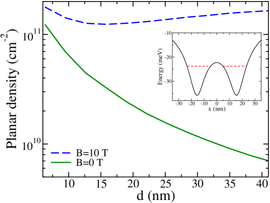
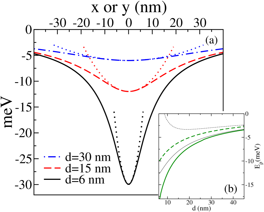
We estimate the maximum planar density of donors () allowed to avoid the formation of a 2DEG as , where is a minimum distance between two donors which is calculated as follows: We assume two donors located at the same distance from the interface and a distance apart. The resulting double well potential along the interface -plane is
| (21) | |||||
as illustrated in the inset of Fig. 13 for nm and nm. We adopt two different criteria to estimate . (i) The first one requires where is the width of the gaussian (see Fig. 5). For instance, for nm, this gives nm leading to cm-2, while for nm, nm and cm-2. (ii) The second criterion, which we find to be slightly more restrictive, requires a high enough barrier within the double well, and is given by
| (22) |
where corresponds to the equality condition. is the double-well 2-dimensional Hamiltonian
| (23) |
with and the kinetic energy terms. is the maximum height of the inter-well barrier, which is required to be above the single-particle expectation value of the energy . The maximum planar density estimated from Eq. (22) is shown in the main panel of Fig. 13. For instance, cm-2 obtained from nm. is larger for the donors closer to the interface. For instance, cm-2 ( nm).
As shown in Fig. 6, decreases with a perpendicular magnetic field, hence increasing the maximum planar density. The first criterion for the maximum planar density gives, for nm and T, nm and cm-2. The second criterion gives the dashed curve in Fig. 13 which is, on average, almost one order of magnitude larger than without a magnetic field. Note that the effect of the magnetic field is much stronger for large distances .
III.2 Qubit interaction at the interface: exchange
One of the problems for quantum computation in doped Si arises from the lack of control of the exact position of the donors. The main consequence of this is the indetermination of the value of the exchange between two neighboring donor electrons due to the theoretically predicted oscillations of exchange with , caused by valley interference effects. Koiller et al. (2002a, b) One straightforward way to alleviate this problem is to perform these operations at the interface Calderón et al. (2006c) where, as discussed in Sec. II.2, this degeneracy is lowered. Additionally, it would be much easier to control the qubit operations when the electrons are at the interface, similar to the successful experiments on double quantum dots in GaAs Petta et al. (2005); Koppens et al. (2005); Johnson et al. (2005); Laird et al. (2006) and Si. Gorman et al. (2005) Note that the potential created by donor pairs (inset in Fig. 13) resembles very much a double quantum dot with the clear advantage that, in this case, the potential is produced exclusively by the Coulomb attraction of the donors and its exact form is known: .
It is therefore of interest to determine the exchange coupling between donor electrons at the interface. As a first approach, we perform these calculations within the Heitler-London method. The validity and limitations of this method to calculate exchange in semiconductor nanostructures has been previously discussed by the authors. Calderón et al. (2006d) The expression for the exchange within this approximation is
where , is the overlap, and is the electron-electron interaction with the distance between electron (1) and electron (2). The first term in Eq. (LABEL:eq:exch) is the direct term and the second is the exchange term.
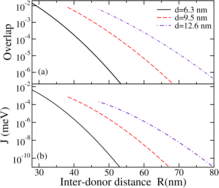
In Fig. 14 we show the exchange and the overlap versus the inter-donor distance for three different values of . Note that the overall dependence of these two quantities with is very similar, indicating that the behavior of is closely related to the overlap.Calderón et al. (2006d) and values are shown only for distances , defined in Sec. III.1. For a wide range of ’s, is of the same order as in GaAs double quantum dots where ’s as low as neV have been measured. Laird et al. (2006)
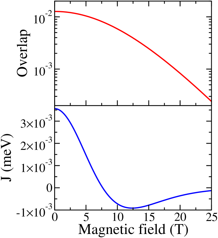
Exchange control can be performed by applying a magnetic field perpendicular to the interface, which reduces the wave-function radius, therefore decreasing the overlap. The effect of the magnetic field on the exchange is well known: Loss and DiVincenzo (1998) decreases and eventually changes sign when the triplet is favored becoming the ground state. This is illustrated in Fig. 15 for nm and nm. At very large fields the singlet and triplet states become degenerate, as expected. Note that, in this case, the qualitative behavior of and with magnetic field is very different.
IV Summary and conclusions
Quantum computer architectures based on semiconductor nanostructure qubits have the key potential advantage of scalability, which has led to the great deal of current interest in Si- and GaAs-based quantum computation. Silicon based spin qubits have the important additional advantage of extremely long spin coherence times ( miliseconds or more) since isotopic purification (eliminating 29Si nuclei) could considerable suppress spectral diffusion induced electron spin decoherence de Sousa and Das Sarma (2003); Tyryshkin et al. (2003); Abe et al. (2004); Witzel et al. (2005); Tyryshkin et al. (2006); Witzel and Das Sarma (2006) leading to ms, whereas electron spin coherence time is constrained to be rather short in GaAs quantum dot structures, s, since neither Ga nor As nuclei have zero nuclear angular momentum isotopes. However, the experimental progress in Si spin qubits has been very slow whereas there has been impressive recent experimental progress in the GaAs quantum dot spin qubits. Petta et al. (2005); Koppens et al. (2005); Johnson et al. (2005); Koppens et al. (2006); Laird et al. (2006) The main experimental advantage of GaAs quantum dot system has been the ease in the 1-qubit and 2-qubit manipulation because the electrons near the surface can be effectively controlled by surface gates. By contrast, Si:P qubits are in the bulk, severely hindering experimental progress since electron manipulation in the bulk has turned out to be a difficult task.
In this paper we show through detailed quantitative theoretical work how to control and manipulate qubits (i.e. both single electrons and two-electron exchange coupling) in a doped-Si quantum computing architecture Kane (1998) by applying external electric and magnetic fields. In particular, we have analyzed three main issues: (i) the times involved in the donor electron ’shuttling’ between the donor and the interface of Si with (typically) SiO2 have been found to be a few orders of magnitude shorter than the spin coherence times in Si, as required to allow for the necessary ’logic operations’ and ’error correction’ to take place; (ii) the existence of a well defined interface state where the electron remains bound and localized, so that it does not spread and form a 2DEG. This condition, which guarantees that electrons actually involved in a particular operation be taken back from the interface to donor sites, leads to a lower bound for the interdonor spacing, and consequently a maximum donor planar density; and (iii) the possibility of performing the two-qubit exchange gate operations at the interface, instead of around the donor sites as originally proposed.Kane (1998) Our results show that sufficiently large values of exchange coupling ( meV) can be achieved.
Interface operations have several potential advantages over bulk operations, the most obvious one being that the read-out procedure would be simplified. A well known limitation of exchange gates for donor electrons in the bulk is the oscillatory behavior of the exchange coupling, which is due to the strong pinning of the six conduction band Bloch-function phases at each donor site, where the Coulomb potential is infinitely attractive.Koiller et al. (2004) This condition is alleviated at the interface in two ways: first, the six valley degeneracy is partially lifted and, second, although the electrons at the interface remain bound to the donors, the binding potential is not singular; it is actually equivalent to a quantum dot potential. Experiments on charge-qubit control in a double quantum dot at Si surface Gorman et al. (2005) indicate that the exchange oscillatory behavior may not be a severe problem for donor-bound electrons manipulated at the Si/SiO2 interface.
Our proposal combines the advantages of Si spin qubits (i.e. long time) with the structural advantages of GaAs qubit control and manipulation. We believe that the specific experiments we propose (and analyze in quantitative details) in this paper, if carried out, will go a long way in establishing the feasibility of a Si quantum computer.
Acknowledgements.
This work is supported by LPS and NSA. B.K. also acknowledges support from CNPq, FUJB, Millenium Institute on Nanotechnology - MCT, and FAPERJ.References
- Kane (1998) B. E. Kane, Nature 393, 133 (1998).
- de Sousa and Das Sarma (2003) R. de Sousa and S. Das Sarma, Phys. Rev. B 68, 115322 (2003).
- Tyryshkin et al. (2003) A. M. Tyryshkin, S. A. Lyon, A. V. Astashkin, and A. M. Raitsimring, Phys. Rev. B 68, 193207 (2003).
- Abe et al. (2004) E. Abe, K. Itoh, J. Isoya, and S.Yamasaki, Phys. Rev. B 70, 033204 (2004).
- Witzel et al. (2005) W. M. Witzel, R. de Sousa, and S. Das Sarma, Phys. Rev. B 72, 161306 (2005).
- Tyryshkin et al. (2006) A. M. Tyryshkin, J. J. L. Morton, S. C. Benjamin, A. Ardavan, G. A. D. Briggs, J. W. Ager, and S. A. Lyon, Journal of Physics: Condensed Matter 18, S783 (2006).
- Witzel and Das Sarma (2006) W. M. Witzel and S. Das Sarma, cond-mat/0604577 (2006).
- Koiller et al. (2002a) B. Koiller, X. Hu, and S. Das Sarma, Phys. Rev. Lett, 88, 027903 (2002a).
- Kane (2005) B. E. Kane, MRS Bulletin 30, 105 (2005).
- Schenkel et al. (2003) T. Schenkel, A. Persaud, S. J. Park, J. Nilsson, J. Bokor, J. A. Liddle, R. Keller, D. H. Schneider, D. W. Cheng, and D. E. Humphries, J. Appl. Phys. 94, 7017 (2003).
- Shinada et al. (2005) T. Shinada, S. Okamoto, T. Kobayashi, and I. Ohdomary, Nature 437, 1128 (2005).
- Jamieson et al. (2005) D. N. Jamieson, C. Yang, T. Hopf, S. M. Hearne, C. I. Pakes, S. Prawer, M. Mitic, E. Gauja, S. E. Andresen, F. E. Hudson, et al., Appl. Phys. Lett. 86, 202101 (2005).
- O’Brien et al. (2001) J. L. O’Brien, S. R. Schofield, M. Y. Simmons, R. G. Clark, A. S. Dzurak, N. J. Curson, B. E. Kane, N. S. McAlpine, M. E. Hawley, and G. W. Brown, Phys. Rev. B 64, 161401 (2001).
- Schofield et al. (2003) S. R. Schofield, N. J. Curson, M. Y. Simmons, F. J. Rueß, T. Hallam, L. Oberbeck, and R. G. Clark, Phys. Rev. Lett. 91, 136104 (2003).
- Loss and DiVincenzo (1998) D. Loss and D. P. DiVincenzo, Phys. Rev. A 57, 120 (1998).
- Vrijen et al. (2000) R. Vrijen, E. Yablonovitch, K. Wang, H.-W. Jiang, A. Balandin, V. Roychowdhury, T. Mor, and D. DiVincenzo, Phys. Rev. A 62, 012306 (2000).
- Levy (2001) J. Levy, Phys. Rev. A 64, 052306 (2001).
- Friesen et al. (2003) M. Friesen, P. Rugheimer, D. E. Savage, M. G. Lagally, D. W. van der Weide, R. Joynt, and M. A. Eriksson, Phys. Rev. B 67, 121301 (2003).
- Hollenberg et al. (2004a) L. C. L. Hollenberg, A. S. Dzurak, C. Wellard, A. R. Hamilton, D. J. Reilly, G. J. Milburn, and R. G. Clark, Phys. Rev. B 69, 113301 (2004a).
- Gorman et al. (2005) J. Gorman, D. G. Hasko, and D. A. Williams, Phys. Rev. Lett. 95, 090502 (2005).
- Rugar et al. (2004) D. Rugar, R. Budakian, H. J. Mamin, and B. W. Chui, Nature 430, 329 (2004).
- Xiao et al. (2004) M. Xiao, I. Martin, E. Yablonovitch, and H. Jiang, Nature 430, 435 (2004).
- Koppens et al. (2006) F. H. L. Koppens, C. Buizert, K. J. Tielrooij, I. T. Vink, K. C. Nowack, T. Meunier, L. P. Kouwenhoven, and L. M. K. Vandersypen, Nature 442, 766 (2006).
- Hollenberg et al. (2004b) L. C. L. Hollenberg, C. J. Wellard, C. I. Pakes, and A. G. Fowler, Phys. Rev. B 69, 233301 (2004b).
- Greentree et al. (2005) A. D. Greentree, A. R. Hamilton, L. C. L. Hollenberg, and R. G. Clark, Phys. Rev. B 71, 113310 (2005).
- Stegner et al. (2006) A. R. Stegner, C. Boehme, H. Huebl, M. Stutzmann, K. Lips, and M. S. Brandt, Nat. Phys. 2, 835 (2006).
- Calderón et al. (2006a) M. Calderón, B. Koiller, and S. Das Sarma, cond-mat/0610089 (2006a).
- Petta et al. (2005) J. R. Petta, A. C. Johnson, J. M. Taylor, E. A. Laird, A. Yacoby, M. D. Lukin, C. M. Marcus, M. P. Hanson, and A. C. Gossard, Science 309, 2180 (2005).
- Koppens et al. (2005) F. H. L. Koppens, J. A. Folk, J. M. Elzerman, R. Hanson, L. H. W. van Beveren, I. T. Vink, H. P. Tranitz, W. Wegscheider, L. P. Kouwenhoven, and L. M. K. Vandersypen, Science 309, 1346 (2005).
- Johnson et al. (2005) A. C. Johnson, J. R. Petta, J. M. Taylor, A. Yacoby, M. D. Lukin, C. M. Marcus, M. P. Hanson, and A. C. Gossard, Nature 435, 925 (2005).
- Laird et al. (2006) E. A. Laird, J. R. Petta, A. C. Johnson, C. M. Marcus, A. Yacoby, M. P. Hanson, and A. C. Gossard, Phys. Rev. Lett. 97, 056801 (2006).
- Koiller et al. (2002b) B. Koiller, X. Hu, and S. Das Sarma, Phys. Rev. B 66, 115201 (2002b).
- Calderón et al. (2006b) M. J. Calderón, B. Koiller, X. Hu, and S. Das Sarma, Phys. Rev. Lett. 96, 096802 (2006b).
- Calderón et al. (2006c) M. J. Calderón, B. Koiller, and S. Das Sarma, Phys. Rev. B 74, 081302 (2006c).
- Kohn (1957) W. Kohn, Solid State Physics Series, vol. 5 (Academic Press, 1957), edited by F. Seitz and D. Turnbull.
- Stern and Howard (1967) F. Stern and W. Howard, Phys. Rev. 163, 816 (1967).
- Martin and Wallis (1978) B. G. Martin and R. F. Wallis, Phys. Rev. B 18, 5644 (1978).
- MacMillen and Landman (1984) D. B. MacMillen and U. Landman, Phys. Rev. B 29, 4524 (1984).
- Ando et al. (1982) T. Ando, A. Fowler, and F. Stern, Rev. Mod. Phys. 54, 437 (1982).
- Stern (1972) F. Stern, Phys. Rev. B 5, 4891 (1972).
- Ferguson et al. (2006) A. J. Ferguson, V. C. Chan, A. R. Hamilton, and R. G. Clark, Appl. Phys. Lett. 88, 162117 (2006).
- Brown et al. (2006) K. R. Brown, L. Sun, and B. E. Kane, Appl. Phys. Lett. 88, 213118 (2006).
- Jacak et al. (1998) L. Jacak, P. Hawrylak, and A. Wójs, Quantum Dots (Springer-Verlag, Berlin, 1998).
- Landau and Lifshitz (1977) L. Landau and E. Lifshitz, Quantum Mechanics (Pergamon, 1977).
- Thilderkvist et al. (1994) A. Thilderkvist, M. Kleverman, G. Grossmann, and H. Grimmeiss, Phys. Rev. B 49, 14270 (1994).
- Martins et al. (2004) A. S. Martins, R. B. Capaz, and B. Koiller, Phys. Rev. B 69, 085320 (2004).
- Messiah (1962) A. Messiah, Quantum Mechanics (John Wiley & Sons, Inc, New York, 1962).
- Ribeiro et al. (2002) F. Ribeiro, R. Capaz, and B. Koiller, Appl. Phys. Lett. 81, 2247 (2002).
- Schenkel et al. (2006) T. Schenkel, A. M. Tyryshkin, R. de Sousa, K. B. Whaley, J. Bokor, J. A. Liddle, A. Persaud, J. Shangkuan, I. Chakarov, and S. A. Lyon, Appl. Phys. Lett. 88, 112101 (2006).
- Hayashi et al. (2003) T. Hayashi, T. Fujusawa, H. D. Cheong, Y. H. Jeong, and Y. Hirayama, Phys. Rev. Lett. 91, 226804 (2003).
- Hu et al. (2005) X. Hu, B. Koiller, and S. Das Sarma, Phys. Rev. B 71, 235332 (2005).
- Calderón et al. (2006d) M. J. Calderón, B. Koiller, and S. Das Sarma, Phys. Rev. B 74, 045310 (2006d).
- Koiller et al. (2004) B. Koiller, R. B. Capaz, X. Hu, and S. Das Sarma, Phys. Rev. B 70, 115207 (2004).