High quality c-axis oriented thin-film obtained at very low pre-heating temperature
Abstract
Highly oriented thin-film has been obtained at a very low pre-heating temperature, with the spin-coating sol-gel technique. The dependence of the c-axis orientation on the pre-heating temperature has been studied with experimental design and response surface techniques to optimize the deposition process with respect to c-axis orientation, and surface uniformity. The optimization variables selected for this study are: pre-heating temperature, spin-coating speed and number of coating layers. The films are probed with X-ray diffraction and electron microscopy.
I Introduction
Zinc oxide thin films exhibit a variety of properties such as: semiconducting (II-VI), photoconducting, piezoelectricity, birefrigence, acousto-optical, transparency in the infrared region, and opto-electrical properties. This makes this material very interesting for theoretical and experimental studies W2004 ; PNIH2005 . films can be produced in various phases, such as: wurtzite (hcp), zincblende (fcc), rocksalt (fcc), cesium chloride (sc) FPM2006 . Under ambient conditions crystallizes in the wurtzite structure, a tetrahedrally coordinated structure with hexagonal lattice. films can crystallize in different orientations as a function of the deposition technology, annealing temperature, substrate, etc. The most common orientation is (hexagonal wurtzite), which presents the densest atomic packing and minimum surface energy ZLZYZ2006 ; AOMGB2004 ; BGK1998 ; LWLYXLC2004 ; CGC2004 ; PBS2003 . Quality of the film is typically determined with regard to transparency, conductivity, crystalline orientation, and surface uniformity. Crystalline orientation is key to achieve thin-film with piezoelectric properties.
Due to its low cost, and capability to coat large surface areas WWCCW2006 , sol-gel is the technique selected for this study. One possible difficulty with sol-gel is the purity of the film, which can affect the electrical and optical properties of the film, due to the high density of carrier traps and potential barriers at grain boundaries LWLYXLC2004 . However, several studies have shown that the optical and electrical properties could be considerably improved by optimized deposition conditions LLZSLZKF2002 ; YLLLLSZF2004 ; YAK2005 ; LLSLZKF2002 ; RI2005 .
Many researchers have prepared zinc oxide thin films with the sol-gel technique. Ohyama et al. OKY1997 studied the crystallization of dip-coated sol-gel deposited films to produce piezoelectric films for SAW applications. They varied the pre-heating temperature from up to , and annealing temperature from up to . They have observed that the pre-heating temperature of dip-coated produced films has a strong effect on the crystal orientation. Their best result is achieved with a pre-heating temperature of . Bao et al. BGK1998 also used sol-gel deposited films and studied the orientation by varying the annealing temperature from up to , which is too high temperature for our application. In the work of Castanedo-Pérez et al PSSMGDA1999 , is used as precursor, they have studied the effect of the annealing temperature from to (pre-heating at ) on the formation of . The film obtained is not highly oriented, as they were concerned with the optical transmission properties of the film. Jiwei et al. JLX2000 deposited films on also with sol-gel with pre-heating at , annealing from up to , the resulting films displayed good orientation. Paul et al PBS2003 used a two-step heat treatment, in air, followed by in furnace, repeating the cycle many times. The annealing was carried out in high vacuum at , with good results. Alam et al AC2001 used dipping solution, pre-heating and annealing from up to , but did not achieve a good orientation of the films. Znaidi ZIBSK2003 studied the dependence of the crystallization on the relative concentration of zinc actetate dihydrate to monoethanolamine. The films were pre-heated at and after finishing the coating cycles, they were annealed at to get oriented films. Chakrabarti et al CGC2004 varied annealing temperature from up to . But their films have not shown good orientation on the various substrates used. Aslan et al. AOMGB2004 achieved good quality films by varying the annealing temperature from up to . Li et al LWLYXLC2004 varied the pre-heating temperature from up to , but their results were reasonable above , annealed at . Zhang et al ZLZYZ2006 has achieved very high quality films by starting the deposition process with a seed layer deposited by PLD. In their work the pre-heating temperature varied from up to , and annealed at . Just recently, came to our attention the work of Wang et al. WWCCW2006 , which also uses the sol-gel method, with pre-heating temperature from up to , and annealing temperature from up to . Almost the same range as in the work of Ohyama et al. OKY1997 , but did not get good results.
Most authors have focused their attention on the effect of the annealing temperature on the crystallization. And have considered high temperatures for the pre-heating cycle.
Our objective is to apply experimental design and response surface techniques to produce highly oriented films, with the lowest thermal bugget possible. The process should be compatible with silicon/silicon-dioxide substrates. Such films can be useful to make piezoelectric coatings for integrated smart sensors. The parameters selected for study are: pre-heating temperature, spin speed and number of coating layers. The paper is divided into four sections, this introduction being the first, next the experimental procedure is described. In the third section, the results and analysis, and finally the conclusions.
II Experimental Procedure
II.1 Materials preparation
Our films were prepared by dissolving zinc acetate dyhidrate, (, Merck), in methanol (, Carlo Erba) under stirring at , until a transparent and homogeneous solution is obtained. The microscope glass substrates are cleaned with neutral cleaning agent in ultrasonic bath for , washed in deionized water, acetone (), deionized water on ultrasonic bath (), isopropanol () and dry nitrogen and preserved in desiccator. The solution is then spun-on onto the substrate. After coating the required number of layers, the thin film is annealed at for . This procedure was performed on glass substrates and on silicon wafers with a silicon dioxide layer.
II.2 Optimization of ZnO thin film
In order to optimize the preparation of c-axis oriented ZnO thin films, experimental design and response surface method are used RI2005 . For this study, two experimental designs have been carried out. The independent variables are: pre-heating temperature, spin-coating speed, and number of coating layers. Relative peak intensity ( AC2001 ) is the dependent variable.
The first experimental design is a linear model factorial central composite design, with three central points. This leads to eleven experiments, which includes factorial points and central points.
After analysis of the variable effects in the first experimental design, another experimental design was prepared to further optimize the process. The second experiment is a quadratic model -full-factorial central composite design, with three central points. This leads to experiments, including star points factorial. Statistical significance of the regression coefficients was determined with the -test analysis of variance (ANOVA), which revealed that the regression is statistically significant at of confidence level ().

III Results and Discussion
The results of Ohyama et al. OKY1997 suggest that the pre-heating temperature of dip-coating produced films have a strong effect on the crystal orientation. Recently, we have found out that, this work was also performed on spin-coating produced films by Wang et al. WWCCW2006 . Both studies used the same temperature range.
Considering that the rate of solvent desorption and drying could have an importante effect on the crystallization, we have decided to investigate this effect by using a lower temperature range for pre-heating. Besides, we are interested in depositing very high quality films onto silicon chips to make SAW and multilayer BAW devices and integrated sensors, this demands the lowest temperature treatment possible.
Following the preparation sequence presented earlier, the resulting films were primarily observed by X-rays diffraction, with () radiation source. The measurements were carried out in the range . The best films were further observed with SEM, JEOL-6460, to exam the surface uniformity and grain size. Considering the effect of the three selected variables (pre-heating temperature, spin-coating speed, and number of coating layers) on the crystallinization of the film. After the first experimental design, it is already clear that the pre-heating temperature is the only statistically significant, , effect. This is also confirmed in the second experimental design.
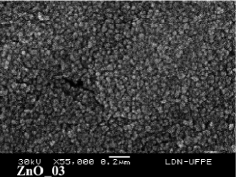
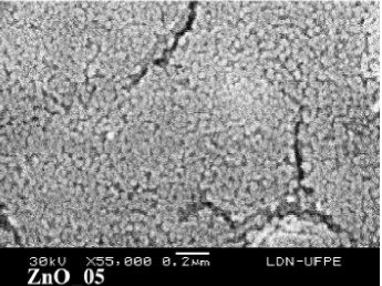
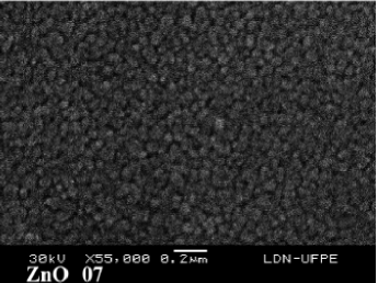
In Figure 1, the X-rays diffraction patterns of thin films are presented. For the X-rays the films are deposited on glass substrates, and annealed at for , in hot plate. Considering the relative peak intensity, the best results for the c-axis orientation are obtained for (pre-heating= , spin speed= and coating layers= ), (pre-heating= , spin speed= and coating layers= ), and (pre-heating= , spin speed= and coating layers= ). The largest intensity of the (002)-peak is observed at conditions , while the largest relative intensity has occurred at conditions . Under the SEM, film has displayed cracks.
| run | Relative peak | FWHM | Grain size |
|---|---|---|---|
| assay | intensity (002) | (degree) | ( (std. dev.)) |
| () | |||
| () | |||
| () |
The films with the optimal conditions also displayed the best uniformity, as shown in Figure 2. The grain size is of the order of , which are compatible with the FWHM measurements, as can be seen in Table 1. The FWHM is approximately for all selected samples. Considering that for the X-rays used, , and using Scherrer’s relation ), the expected grain size is about , which is close to the observed value.
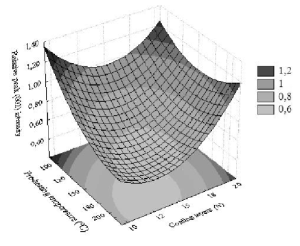
Considering the relative peak intensity, a response surface plot was prepared. The plot as a function of pre-heating temperature and number of coating layers is presented in Figure 3. One can see that for a low pre-heating temperature, it is possible to get high quality film almos independent of film thickness.
IV Conclusions
The methodology of experimental design and response surface analysis is used to find the optimum process parameters for the preparation of the c-axis oriented thin films with sol-gel. In particular, it has been shown that the pre-heating temperature plays an important role in the preparation thin films with high c-axis orientation. Considering the range used the optimal condition parameters are: pre-heating= , spin speed= and coating layers= . With such conditions the highest relative peak intensity is achieved. We have successfully deposited c-axis oriented zinc oxide thin films on glass substrate from zinc acetate by inexpensive sol-gel process using low annealing temperature (). The process was also repeated on silicon dioxide. This result is very interesting for the integration of thin films for the construction of integrated smart sensors.
Acknowledgments
The authors thank Prof. J. A. O. de Aguiar for the X-rays measurements. We also acknowledge the financial support of FINEP and PETROBRAS. One of the authors (A.M.P.S.) also acknowledges the support of CNPq/FACEPE.
References
- (1) Z. L. Wang, J. of Phys.:Condens. Matter 16 (2004) R829-858.
- (2) S. J. Perton, D. P. Norton, K. Ip, Y. W. Heo, T. Steiner, Progress in Materials Science, 50 (2005) 293-340.
- (3) A. Fouchet, W. Prellier, B. Mercey, cond-mat/0604468 (2006).
- (4) C.-Y. Zhang, X.-M. Li, X. Zhang, W.-D. Yu, J.-L. Zhao, Journal of Crystal Growth, 290 (2006) 67-72.
- (5) M. H. Aslan, A. Y. Oral, E. Menşur, A. Gül, E. Başaran, Solar Energy Material & Solar Cells 81 (2004) 543-552.
- (6) D. Bao, H. Gu, A. Kuang, Thin Solid Films 312 (1998) 37-39.
- (7) H. Li, J. Wang, H. Liu, C. Yand, H. Xu, X. Li, H. Cui, Vacuum 72 (2004) 57-62.
- (8) S. Chakrabarti, D. Ganguli, S. Chandhuri, Materials Letters, 58 (2004) 3952-3957.
- (9) G. K. Paul, S. Bandyopadhyay, S. K. Sen, S. Sen, Materials Chemistry and Physics 79 (2003) 71-75.
- (10) B. S. Li, Y. C. Liu, Z. Z. Zhi, D. Z. Shen, Y. M. Liu, J. Y. Zhang, X. G. Kong, X. W. Fan, Thin Solid Films 414 (2002) 170-174.
- (11) J. F. Yan, Y. M. Lu, Y. C. Liu, H. W. Liang, B. H. Li, D. Z. Shen, J. Y. Zhang, X. W. Fan, Journal Crystal Growth 266 (2004) 505-510.
- (12) A. Yamamoto, S. Atsuta, Y. Kanemitsu, Physica E 26 (2005) 96-99.
- (13) B. S. Li, Y. C. Liu, D. Z. Shen, Y. M. Lu, J. Y. Zhang, X. G. Kong, X. W. Fan, Z. Z. Zhi, Journal Vacuum Technology A 20(1), Jan/Feb (2002) 265-269.
- (14) M. I. Rodrigues, A. F. Iemma,(2005) Planejamento de Experimentos e Otimização de Process, 1st Edition, Casa do Pão Editora, Campinas, SP.
- (15) M. Ohyama, H. Kozuka, T. Yoko, Thin Solid Films, 306 (1997) 78-85
- (16) M. Wang, H. Wang, W. Chen, Y. Chui, L. Wang, Materials C hemistry and Physics 97 (2006) 219-225.
- (17) R. Castanedo-Pérez, O. Jiménez-Sandoval, S. Jiménez-Sandoval, J. Márquez-Marín, A. Mendoza-Galván, G. Torres-Delgado, A. Maldonado-Alvarez, J. Vac. Sci. Technol. A 17 (1999) 1811-1816
- (18) Z. Jiwei, Z. Liangying, Y. Xi, Ceramics International 26 (2000) 883-885.
- (19) M. J. Alam, D. C. Cameron, J. Vac. Sci. Technol. 19 (2001) 1642-1646
- (20) L. Znaidi, G. J. A. A. Soler Illia, S. Benyahia, C. Sanchez, A. V. Karaev, Thin Solid Films 428 (2003) 257-262.