Magnetic-field effects on transport in carbon nanotube junctions
Abstract
Here we address a theoretical study on the behaviour of electronic states of heterojunctions and quantum dots based on carbon nanotubes under magnetic fields. Emphasis is put on the analysis of the local density of states, the conductance, and on the characteristic curves of current versus voltage. The heterostructures are modeled by joining zigzag tubes through single pentagon-heptagon pair defects, and described within a simple tight binding calculation. The conductance is calculated using the Landauer formula in the Green functions formalism. The used theoretical approach incorporates the atomic details of the topological defects by performing an energy relaxation via Monte Carlo calculation. The effect of a magnetic field on the conductance gap of the system is investigated and compared to those of isolated constituent tubes. It is found that the conductance gap of the studied CNHs exhibits oscillations as a function of the magnetic flux. However, unlike the pristine tubes case, they are not Aharonov-Bohm periodic oscillations.
I Introduction
Following the richness possibilities explored first by the semiconducting physicists, heterostructures made of carbon nanotubes (CNs) have recently also been studied. In particular, the combination of two or more kind of pristine tubes offers a variety of physical situation mainly due to the intrinsical feature of the carbon tubes, which exhibit electronic properties dictated by geometrical aspectsDresselhaus . This fact, together with quite important mechanical characteristics, make clear that CNs may be used in different devices in science and nanotechnologyTans ; Choi ; Wie . The presence of topological defects can change the chirality of the CNs. It was shown that local curvature and tube diameter do not suffer a drastic change when the defect is a pentagon-heptagon pairDunlap ; Charlier . Actually, with this kind of defect it is possible to join two different CNs forming a heterostructure similar to the semiconducting ones largely studiedTAndo . Metal-metal and metal-semiconductingFerreira ; Chico1 ; Ouyang ; Hu ; Fa systems may be naturally formed besides the standard semiconducting composites. Of course, the electronic nature of each one of the CN components and their symmetries will define the electronic and transport properties exhibited by the resulting heterostruturesChico2 ; Dresse ; Tamura ; Yao ; Yang ; Farajian . For zigzag CNs, a change in one unity in the chiral number n [(n-1, 0) or (n+1, 0)] leads to an electronic changing from semiconductor to metallic electronic behavior and vice-versa, involving a small change in the diameter of the tubes. Similar effect may be achieved by applying a magnetic field to the carbon nanotube heterostructures (CNH’s), showing novel electronics and transport behaviorsNakanishi ; Lee ; Dresse3 ; Fujiwara ; Rocha . By scanning tunneling spectroscopy measurements at selected locations of CNs it is possible to obtain a map of the electronic density of states. This technique allowed the characterization of interface states induced by the presence of defects at the junctions of two semiconducting nanotubesKim , and also the determination of spatial oscillation in the electronic density of states with the period of atomic lattice.
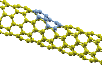
Here we explore the gap energy modulation of nanotube heterostructures (single junctions and quantum dots) under the action of an external magnetic field. Emphasis is put on the transport response dependence. Single junctions have been proved to be stable and in particular the stability of a (7,0)/(6,0) CNH is verified, in the absence of magnetic fields, by calculating the total energy of the system via a numerical Monte Carlo analysis. Fig.1 shows the atomic configuration of this particular heterostructure, adopting a Tersoff empirical interatomic potentialTersoff . The topological defect (a pair of pentagon-heptagon) is marked with bold lines (blue on-line). Despite of the simplicity of the potential-model, it has been properly used for carbon-based materials in the determination of total and defect energy deviations, and elastic properties. The resulted equilibrium atomic position help us in determining the Peierl’s phases when considering the magnetic field since they depend on each one of the atomic positions.
To investigate how the magnetic field changes the electronic properties of the heterostructures, we calculate local density of states (LDOS) and electrical conductance. We consider a single -band tight binding Hamiltonian and follow real-space renormalization techniques. The conductance is calculated using the Landauer formula in the Green function formalismNardelli . We restrict our discussion to zigzag CNs junctions formed by the presence of the pair defects, as shown in figure 1. The external magnetic field is considered uniform and parallel to the system axis. The occurrence of the Aharonov-Bohm effect is investigated in the composed nanostructures.
II Theoretical method
We restrict our present study to (n,0)/(n1,0) carbon nanotube junctions (CNHs), and adopt a single -band tight binding Hamiltonian, taking into account a fixed value for the hopping parameter ( 2.75 eV), independent of the orientation, location and length of the bond. The systems are described in a real space picture which allow us to incorporate the potential fluctuations at the microscopic scale. LDOS and conductance of the structures are calculated within the Green function formalism, employing decimation proceduresFerreira ; Rocha (or, equivalently, ad-layers schemes).
The LDOS at site i is obtained directly from the renormalized locator Gi,i []. The surface Green s functions matching formalism is used to obtain the conductance combined with an iterative calculation of transfer matricesNardelli . Within this picture the full system is partitioned into three parts: the central one and two leads composed of two carbon nanotubes. The conductance is related to the scattering properties of the region via the Landauer formula. In the linear response approach it can be written in term of the Green’s function of the system byGarcia
| (1) |
where is the transmission function of an electron crossing through a central conductor, given by , with Tr being the matricial trace function, the retarded and advanced Green functions corresponding to the central part of the system, and with
| (2) |
describing the coupling between the central part and the right and left leads, given by the corresponding self-energies. Here the contacts are given by surface Green functions corresponding to the (n,0) and (n 1,0) tubes whereas the conductor is the defective ring. All the Green functions are obtained numerically and the effects of the magnetic field are described within the Peierl’s phase approximation. In this scheme the hopping energies are modified by a phase which depends on the potential vector associated with the field and on the relative atomic distances. One should stress that the atomic positions of the structure, including the defect region, were carefully studied using Tersoff Tersoff relaxation process. In what follows, the energies are written in terms of the hopping parameter , the magnetic fluxes in units of the quantum flux , and taking into account the flux through the biggest tube of the heterostructures. The Fermi level was taken as the zero of the energies.
III Results
Two kinds of structures are considered in this work: a single junction and a semiconductor nanotube quantum dot (CNQD). Both are formed by the presence of the pentagon-heptagon defects. Results for their electronic and transport properties are shown in the following subsections where we discuss the effects on a magnetic field threading the structure.
III.1 Single junctions
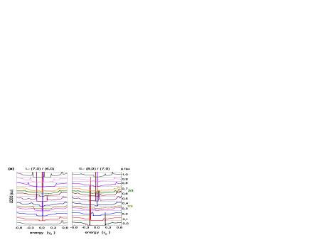
CNH’s of type (n,0)/(n1,0) allow us to consider two types of junctions: semiconductor-metal (S/M) and semiconductor-semiconductor (S/S) configurations. Results for LDOS and conductance for a S/M [(7,0)/(6,0)] and a S/S [(8,0)/(7,0)] junctions are displayed in Fig.2, for different magnetic field intensities. The plotted LDOS are mean values calculated at the defective ring at which the constituent tubes change their diameter. At zero field, the LDOS of the S/M junction [(7,0)/(6,0)] exhibits a plateau close to the Fermi level, whereas the S/S [(8,0)/(7,0)] junction essentially retains the gap of the pristine (7,0). The topological defect produces the apparition of interface states in the LDOS of the S/S junction, localized close to the gap edgeCharlier ; Ferreira ; Rocha ; Liu [see figure 2(a)]. Both studied junctions present a wide gap in the conductance produced basically by the lost of the rotational symmetry in the defective ringChico2 ; Rocha .
——
The behavior of the electronic properties of the CNH’s are analyzed when the magnetic field is turned on, increasing up to one quantum flux. It is clear that, once the magnetic field is turned on, the energy gap is strongly affected, reflecting the sensitivity of the junctions to the presence of field. For magnetic fluxes equal to 1/3 and 2/3 /, the LDOS of both studied junctions shows a metal-insulator-like electronic transition. However, as one can see in figure 2(b), those states close to the Fermi energy do not contribute to the electronic conductance of the system. This is because they are quasi-localized states and not resonant states (which was verified by means of a detailed sweeping of the LDOS in the vicinity of the junction). The presence of the topological defect produces a strong mismatch between right and left electronic wave functions, giving a null transmission probability through the junction, even in the presence of the magnetic field.
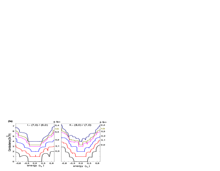
For helping to understand the behavior of the CNH electronic conductance on the magnetic field, we explicitly plot in Fig.3 the conductance gap as a function of a magnetic flux, for the different studied junctions. In all cases the magnetic flux considered has been calculated using the area of the biggest tube composing the CNH’s. Actually, the smaller tubes feel a renormalized flux, scaled by a factor , with being the (n,0)tube radius. Localized states within the gap have been ignored as they may be viewed as states of null width. A well-known result concerned to pristine straight tubes under magnetic field is that they exhibit, metal-insulator-like transitions. Metallic tubes open gaps as soon as a magnetic flux starts threading it (the maximum gap occurring at a half of a quantum flux). On the other hand, a semiconducting tube closes its intrinsic gap at 1/3 and 2/3 of a quantum fluxAndo2 . An Aharonov Bohm (AB)-type effect for the gap size has been predicted and may be written in terms of the tube gap at null fieldLu . The possibility of similar AB effect occurrence for the studied CNH’s was not been observed. For both CNH’s (S/S and S/M) it is found that the conductance gap of the structures is given essentially by the biggest gap of the two constituent tubes, which evolves with the magnetic flux. Similar results have been obtained for other S/S and M/S junctions.
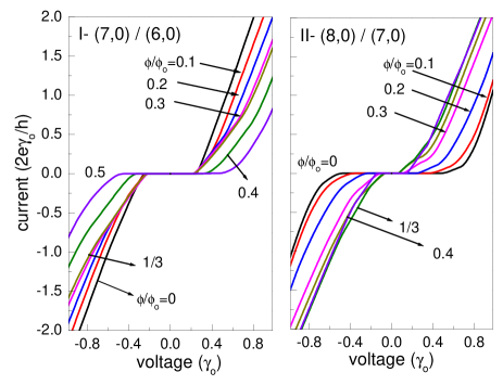
The characteristic curves of current versus applied bias for the studied S/M and S/S junctions are shown in Fig.4, for different magnetic flux intensities. The current across the junction is obtained via the integration of the transmission function, taking into account the Fermi distribution of both leads and assuming that the total potential drop along the heterostructure (bias equal to V) was fully restricted to the junction extension, linking both tubesFaraj . Within this scheme, an extra potential energy was added in the diagonal term (site energy) of the tight binding Hamiltonian. Alternatively, one may use the Keldysh formalism based on non-equilibrium Green functionsKeldysh ; Carioli ; Meir to calculate the transport properties in the non-linear regime. Actually, both treatments are equivalent for coherent transport. For zero magnetic flux the current gap size of the CNH’s is given by the mean value of the gap energies of the individual tubes. Ohmic curves are then not expected for this type of nanotube heterostructure which always involves a semiconducting part. It is easy to show that the minimum gap size is achieved for a M/S structure, being equal to , with the semiconducting gap energy. Besides the band energy shift imposed by the applied voltage, a further confinement effect is noticed when a magnetic flux threads the structure.
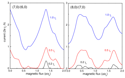
As it is well known, the field lifts the degeneracy of the electronic states. However, differently from the case of pristine tubes, where the semi-classic electronic orbits are split leading to periodic constructive and destructive quantum interference phenomena, the CNH’s do not exhibit oscillatory current behavior. The dependence of the current on the magnetic flux for fixed voltages may prove this issue, as it is shown in Fig.5. The AB period given by one quantum flux, observed in pristine CN’s, is destroyed. Otherwise, general features marked by peaks and valleys in the current curves are preserved for different bias intensities, although exhibiting higher current values as the bias voltage increases. Also remarkable are the differences between the current behavior of both considered CNHs, mainly concerned to the magnetic flux range in which they exhibit a metallic or a semiconducting character. All theses points emphasize the role played by magnetic and electric fields on modifying the physical properties of nanotube structures which may be used to manipulate properly their responses and potential uses in nanoelectronics.
III.2 Nanotube quantum dot
Heterojunctions, such as the discussed ones (n,0)/(n-1,0) are now put together forming a nanotube based quantum dot. The size of the dot is defined by the number of rings forming the internal tube given here by the integer N, . Results for the conductance of CNQD in the absence of a magnetic flux, are presented in Fig.6, considering dots composed of 2, 6 and 10 rings in the internal part, within the leads.
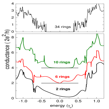
In the upper panel, we show the conductance for a CNQD with N=34 rings. Similarly to the case of single junctions, the electron-hole symmetry is lost for the quantum dot structure due to the topological defects at the interfaces of the (5,0) and (6,0) tubes. As expected, a clean gap is obtained, similar to the semiconducting gap of the (5,0) pristine CN. The CNQD conductance-gap decreases with the size of the dot. In this example, the minimum value for the gap has been obtained for N=6, in which case zero conductance is only achieved at the Fermi energy. Applying a small gate voltage a metallic behavior for the CNQD can be obtained. In particular, for a N=2 dot (length equal to ), there is a non-null conductance at the energy region close to the Fermi level due to the overlap between the metallic wave functions of the leads across the small dot region.
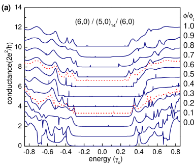
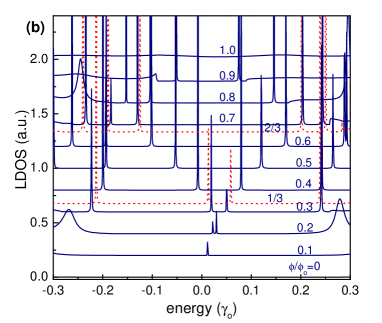
The dependence of the conductance gap on the magnetic field, for a semiconducting (6,0/(5,0)14/(6,0) CNQD is shown in Fig. 7(a). For this particular dot, a conductance gap is always present for different magnetic fluxes, in contrast to the case of a pristine (5,0) tube for which the gap closes for magnetic fluxes equal to 1/3 and 2/3 (dashed curves in the figure). Usually, two kind of states can be distinguished for CNQDs: interface and resonant states. The nature of such states may be determined, for instance, by performing an accurate sweeping of the LDOS within the dot region. This region includes the interface defective rings and also a few rings within the leadsChico1 ; Rocha .
Interface states are typically localized within the energy range close to the Fermi level and have a weak dependence on magnetic field intensity. The resonant states are at energies out of the CN gap region ( in the present example, corresponding to the approximate gap energy at zero magnetic field, for a (5,0) tube). For null field, this particular CNQD structure does not exhibit localized levels in the gap region, as can be seen in the LDOS displayed in figure 7(b). However, as the field is turned on, the LDOS clearly shows that localized states appear close to the Fermi energy, and that they oscillates as a function of the magnetic field.
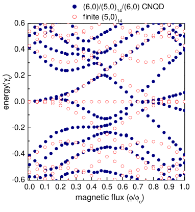
The explicit dependence of the energy states on the magnetic flux is shown in Fig. 8, with full dot symbols. We have also added, for comparison, the results for a finite short (5,0) CN, composed of 14 rings (empty dots). One should noticed that in this case the results are presented as a function of the magnetic flux threading a (5,0) tube, to allow the comparison, whereas for the LDOS exhibited in fig. 7(b) the used magnetic fluxes correspond to the bigger (6,0) tube. The finite tube energy spectrum shows states with energies near the Fermi energy corresponding to edge states whose wavefunctions are localized at both ends of the finite tube Sasaki . As expected, the edge state pinned at the Fermi energy, appearing for the finite CN, is not present in the energy spectrum of the infinite quantum dot heterostructure. The magnetic-field induced defect states of the CNQD, shown in figure 7 (b) as the peaked structures in the LDOS, present quite similar dependence on the magnetic field as the states of the finite tube. They may be considered as edge-like states that are lift by the magnetic field due to the extra confinement imposed by the field. It is also evident the lack of electron-hole symmetry in the spectra of the CNQD as the magnetic field increases, due to the presence of topological defects. Depending on the length and diameter of the dot, and also on the atomic details of the junction, different constituent tubes may be matched, forming different CNQDs. These geometrical aspects will dictate the presence and nature of the electronic states which, in turn, may be modulate by the magnetic flux threading the structures.
IV Summary
We have calculated local density of states and conductance of different heterostructures (single junctions and nanotube quantum dots) under the influence of magnetic fields. Emphasis was put on analyzing the gap modulation induced by the magnetic flux threading the structures and how the geometric details of the individual tubes composing the systems may affect the transport responses. Differently from the pristine tubes, the conductance gaps of the studied CNHs do not exhibit AB-like periodic oscillations as a function of the magnetic flux. This lack of periodicity was also found for the characteristic curves current versus voltage. By comparing the field dependence of the states of the dot structure with the corresponding states of the finite tube (central part of the dot) we were able to identify the nature of particular electronic states appearing in the energy range close to the Fermi level. The used theoretical approach incorporates the atomic details of the topological defects by performing an energy relaxation via Monte Carlo calculation. A theoretical treatment taking into account the charge fluctuations imposed by external bias is presently being studied. We believe that this kind of theoretical studies on nanotube composed systems, together with the fast development on new synthesis techniques, should help to control and modulate the physical responses of these nanostructures.
V Acknowledgments
This work was supported by the Brazilian Agencies CNPq, CAPES, FAPERJ, Instituto do Milênio, and PRONEX-CNPq-FAPERJ grant 171.168-200, also by the Iniciativa Cientifica Milenio P02-054-F, Fondecyt 1050521 and 7060290, and Andes Foundation under the project C-14055/20, and by the Science Foundation Ireland (SFI).
References
- (1) Electronic address: latge@if.uff.br
- (2) R. Saito, G. Dresselhaus, and M. S. Dresselhaus, Physical Properties of Carbon Nanotubes, Imperial College Press London, 1998.
- (3) S. J. Tans, A. Verschueren, and C. Dekker, Nature 393, 49-52 (1998).
- (4) W. B. Choi, D. S. Chung, J. H. Kang, H. Y. Kim, Y. W. Jin, I. T. Han, Y. H. Lee, J. E. Jung, N. S. Lee, G. S. Park, and J. M. Kim, Appl. Phys. Lett., 75, 3129 (1999).
- (5) J. Wie, D. Wu, and H. Zhu, Appl. Phys. Lett., 84, 4869 (2004).
- (6) B. Dunlap, Phys. Rev. B 49, 5643 (1994).
- (7) J. C. Charlier, T. W. Ebbesen, and Ph. Lambim, Phys. Rev. B 53, 11108 (1996).
- (8) T. Ando, Y. Arakama, K. Furuya, S. Komiyana, and H. Nakashima, Mesoscopic Physics and Electronics, Springer, New York 1998.
- (9) M. Ferreira, T. Dargam, R. Muniz, and A. Latgé, Phys. Rev. B 62, 16040 (2000).
- (10) L. Chico, V. H. Crespi, L. X. Benedict, S. G. Louie, and M. L. Cohen, Phys. Rev. Lett. 76, 971 (1996).
- (11) M. Ouyang, J. L. Huang , C. L. Cheung, and C. M. Lieber, Science 291, 97-100 (2001).
- (12) H. F. Hu, Y. B. Li, and H. B. He, Diamond and Related Materials 10, 1818 (2001).
- (13) W. Fa, J. Chen, H. Liu, and J. Dong, Phys. Rev. B 69, 235413 (2004).
- (14) L. Chico, L. X. Benedict, S. G. Louie, and M. L. Cohen, Phys. Rev. B 54, 2600 (1996).
- (15) R. Saito, G. Dresselhaus, and M. S. Dresselhaus, Phys. Rev. B 53, 2044 (1996).
- (16) R. Tamura and M. Tsukada, Phys. Rev. B 55, 4991 (1997).
- (17) Z. Yao, H. Postma, L. Balents and C. Dekker, Nature 402, 273 (1999).
- (18) L. Yang, J. Chen, H. Yang, and J. Dong, Eur. Phys. J. B 33, 215-219 (2003).
- (19) A. Farajian, H. Mizuseki, and Y. Kawazoe, Physica E 22, 675-678 (2004).
- (20) T. Nakanishi and T. Ando, Physica B 249, 136-139 (1998).
- (21) J. -O. Lee, J. -R. Kim, J. -J. Kim, J. Kim, N. Kim, J. W. Park and K. -H. Yoo, Solid State Communication 115, 467-471 (2000).
- (22) S. Roche, G. Dresselhaus, M. S. Dresselhaus, and R. Saito, Phys. Rev B 62, 16092 (2000).
- (23) A. Fujiwara, K. Tomiyama, H. Suematsu, K. Uchida, and M. Yumura, Physica B 298, 541 (2001).
- (24) C. G. Rocha, A. Latgé, and L. Chico, Phys. Rev. B 72, 085419 (2005).
- (25) H. Kim, J. Lee, S. Lee, and Y. Kuk, Phys. Rev B 71, 235402 (2005).
- (26) J. Tersoff, Phys. Rev. Lett 61, 2879 (1988); ibidem Phys. Rev. B 37, 6991 (1988).
- (27) M. Nardelli, Phys. Rev B 60, 7828 (1999).
- (28) F. Garcia-Moliner and V.R. Velasco, Theory of Single and Multiple Interfaces, World Scientific, Singapore (1992).
- (29) H. Liu and Y. Tao, Nanotechnology 16, 619 (2005).
- (30) H.Ajiki and T. Ando, Jour. of the Phys. Soc. of Japan 62, 1255 (1993).
- (31) A. A. Farajian, K. Esfarjani, and Y. Kawazoe, Phys. Rev. Lett. 82, 5084 (1999); A. A. Farajian, K. Esfarjani, and M. Mikami, Phys. Rev. B 65, 165415 (2002).
- (32) L. V. Keldysh, Soviet Physics JETP 20, 1019 (1965).
- (33) C. Carioli, R. Combescot, P. Nozieres, and D. S.-James, Journ. Phys. C: Sol. Stat. Phys. 4, 916 (1971).
- (34) Y. Meir and N. Wingreen, Phys. Rev. Lett. 68, 2512 (1992).
- (35) K. Sasaki, S. Murakami, R. saito, and Y. Kawazoe, Phys. Rev. B 71, 195401 (2005).
- (36) J.P. Lu, Phys. Rev. Lett. 74, 1123 (1997).