First-principles study of the Young’s modulus of Si 001 nanowires
Abstract
We report the results of first-principles density functional theory calculations of the Young’s modulus and other mechanical properties of hydrogen-passivated Si 001 nanowires. The nanowires are taken to have predominantly {100} surfaces, with small {110} facets. The Young’s modulus, the equilibrium length and the residual stress of a series of prismatic wires are found to have a size dependence that scales like the surface area to volume ratio for all but the smallest wires. We analyze the physical origin of the size dependence, and compare the results to two existing models.
pacs:
62.25.+g, 68.35.Gy, 85.85.+jNanoscale mechanical devices have been proposed for applications ranging from nano-electro-mechanical systems (NEMS) such as high frequency oscillators and filtersSiResonators1 to nanoscale probesnanotubeProbe to nanofluidic valvesWAG to q-bits for quantum computationClelandGeller . The process of design and fabrication of these devices is extremely challenging, complicated in part by uncertainties about how even ideal devices should behave. The mechanical response of structures at the nanoscale is known to be different than that of their macroscopic analogs and surface effects in these high surface-to-volume devices are importantCahn , but a predictive theory of nanomechanics remains an open problem.
Much of what is known about mechanics of nanodevices has been learned from atomistic calculations based on empirical potentials. The first such calculations were done for single-crystal alpha quartz beams, finding that the Young’s modulus decreased with decreasing sizeBMVK ; quartzResonators . These and calculations of the Young’s modulus for various other materials have found a size-dependent modulus with an additive correction to the bulk value that scales like the surface area to volume ratioMiller ; RuddIJMSE . A few studies claim an additional contribution that scales like the edge to volume ratio (cf. BMVK, ), and such a contribution, with a factor of the logarithm of the separation of the edges, has been discussed for epitaxial quantum dotsShchukin ; RuddQDot . An intuitive way of understanding these effects is that there is a layer of material at the surface (and edges) whose mechanical properties differ from those of the bulk including different elastic moduli and eigenstrains. This layer could be chemically distinct from the bulk, such as an oxide layer or a hydrogen-passivated surface, but the effect may be entirely due to the structural difference at the surface, such as a bare reconstructed surface. The formalism of nanoscale mechanics based on the surface energy and its first two strain derivatives (the surface stress and modulus) has been developedMiller ; Kukta . Recently it has been proposed that the size dependence of the Young’s modulus can be due to the anharmonicity (non-linearity) of the bulk elastic moduli together with the strain resulting from the surface stressbulkAnharmonicity .
To date experimental data on the size dependence of nanostructure mechanics are very limited. Atomic force microscopy (AFM) measurements of the Young’s modulus ()LieberMechanics of cast metallic nanowires show a strong size dependenceCuenot . Recent experiments have also found a strong size dependence for of ZnO nanowiresZnOnanowire , and other mechanical properties of ZnO and GaN nanowiresNixnanowire . Measurements of for silica nanobeams have demonstrated that the way in which the beam is clamped (i.e. the boundary conditions) affects the apparent valueRuoff2 . A study using a different AFM technique reported a value of of GPa for a nm Si [100] nanowireKizuka ; for 100-200 nm Si111 wires, has been found to be consistent with the bulk valuePYangSiNW . Experimental challenges measuring the intrinsic nanoscale Young’s modulus make this a topic of continued activity, leveraging earlier work on the mechanics of nanotubesnanotubeMech .
In the absence of definitive experimental data, first-principles quantum mechanical calculations can provide robust predictions of nanowire mechanical properties, but few results have been reported. One quantum study based on an empirical tight-binding technique has been publishedArias . The electronic and optical properties of nanowires have been studied using first-principles techniques, leading to interesting predictions about size-dependent phenomena as evidenced by an increase in band gap due to quantum confinementconfinement1 ; confinement2 and a switch from an indirect, to a direct, band gapelectronicSiNW1 ; electronicSiNW2 . We are not aware of any ab initio calculations of nanowire moduli.
Here we present first-principles calculations of the mechanical properties of silicon nanowires, studying the Young’s modulus due to its direct relevance in the function of nanoscale devices such as flexural-mode mechanical resonatorsSiResonators1 and as an archetype for a variety of mechanical properties. We address several important open questions in nanomechanics. Is the modulus size dependent? Does it soften or stiffen at the nanoscale? What physics cause the effect? We focus on prismatic Si 001 nanowires with a combination of 100 and 110 H-passivated surfaces, and single crystal cores as in experimentSiResonators1 ; SiResonators2 . We have chosen the [001] orientation for the longitudinal axis because of its relevance to the NEMS devicesSiResonators1 ; Si nanowires grown rather than etched typically have different orientationsLieber . Hydrogen passivation results from rinsing the oxidized Si surfaces with HF, and it provides a standard system suitable for a systematic study of size dependence in nanomechanics. With other surface conditions the band gap can vary greatly, and nanowires can go from semiconducting to metallicmetallicSiNW ; but the H-passivated wires remain semiconductingSiNWSurface and the surfaces do not change the nature of Si-Si chemical bonding from its covalent character.
First-principles density functional theory (DFT) has been employed: specifically, the Vienna Ab-initio Simulation Package using the projector augmented-wave methodPAW1 ; PAW2 within the generalized gradient approximation (GGA)GGA . The energy cutoff for the plane wave expansion is 29.34 Ry and higher, and 6 points in the one-dimensional irreducible Brillouin zone are used for k-point sampling. Each supercell is periodic, is one Si cubic unit cell long along the wire and has more than 10 Å vacuum space in the transverse directions.
To calculate , we define the cross-sectional area to be the area bounded by the centers of the outermost (H) atoms. This choice is motivated by the fact that the volume excluded by the wire from access by outside atoms is determined from the forces arising from electron interactions. Most of the electron density is enclosed by the boundary formed by H atoms and the electron density from Si atoms essentially vanishes beyond this point. The positions of the nuclei are well defined and not subjective. Other definitions of the bounding surface exist, for example the mid-plane between two identical H-passivated surfaces at their minimum energy separationSiSlabs .
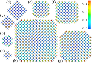
The cross-sectional shape of the Si [001] wire is a truncated square with four 100 facets and four 110 facets. Some wires studied have no 100 facets; for those that do, the ratio of the facet areas is taken to be roughly in accordance with the Wulff shape for a bare wire with (110)-(1x1) and (100)-p(2x2) surface reconstructions; i.e. the ratio of 100 to 110 area is 3.5:1. For each of the nanowire geometries shown in Fig. 1, the Si atoms were initially positioned at their bulk lattice sites and hydrogens were added to terminate the bonds at the surfaces, and this configuration was relaxed. The system was relaxed to its zero-temperature minimum energy with the length of the periodic supercell held fixed at the bulk value in the longitudinal direction. The axial stress in this configuration, where is the DFT total energy, is indicative of the residual stress in a doubly clamped beam etched from a single-crystal substrate. It is plotted in Fig. 2.
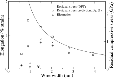
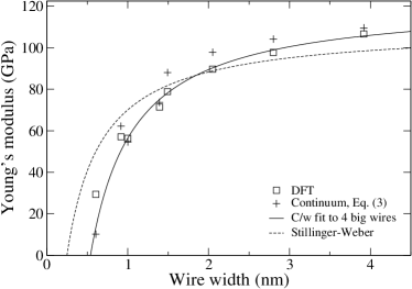
Next the relaxed total energy was calculated for each wire in a series of longitudinal strains, at increments of roughly 0.5%. These total energy values were fit to a polynomial. The minimum of the polynomial gives the equilibrium length, and the value of the curvature at the minimum gives the Young’s modulus, . The equilibrium elongation and modulus are plotted in Figs. 2 and 3, respectively.
The calculated Young’s modulus of the 1.49 nm wire is tabulated in Table 1. The table gives an indication of the sensitivity to the order of the polynomial fit. For the given order, a higher cutoff energy offers little improvement. We find that the second order fit with 29.34 Ry energy cutoff is reasonably good, differing by less than 2% compared with all the higher-order combinations tested. The second-order fit also permits direct comparison with the results from bigger wires where the number of data points and the energy cut off are limited by the computational cost of systems up to 405 Si and 100 H atoms.
| Cutoff energy | Order of polynomial fitting | ||||
| (Ry) | 2nd | 3rd | 4th | 5th | 6th |
| 29.34 | 78.90 | 78.88 | 79.90 | 79.94 | 78.61 |
| 44.10 | 79.31 | 79.28 | 80.39 | 80.33 | 78.95 |
| 51.45 | 79.40 | 79.37 | 80.35 | 80.31 | 79.01 |
These calculations allow us to analyze the physical origin of the size dependence. Size dependences of the residual stress and the elongation evident in Fig. 2 are driven by the same physics: compressive surface stress. The residual axial stress of the Si beam may be decomposed into core, H adatom and Si surface parts: core contributions from the Si atoms, extrinsic contributions from hydrogen (H-H) interactions and intrinsic surface contributions from the change to the Si bonds near the surface compared to the Si bulk (Si-H and modified bond order Si-Si). Since DFT only provides a total energy, this decomposition is somewhat ambiguous. We estimate the H-H interactions as equal to those of neighboring hydrogens in two silane molecules in the orientation and separation of the H-passivated surface, and the core contribution to be the axial stress in bulk Si uniformly strained to match the nanowire; the intrinsic contribution is the remainder. The extrinsic contribution is most important, as we now show. The intrinsic surface stress is small, as expected since the dangling Si bonds are well terminated with H and the Si-Si bond order is not significantly different than in the bulk. The small magnitude of the intrinsic stress is best seen in the case of the 1.39 nm wire for which the elongation is less than 0.1% compared to 1.5% of the 1.49 nm wire. The absence of 100 facets on this wire leads to a small extrinsic stress since the H-H separation on the 110 facets is relatively large. The vacant Si sites above the facets are filled by one and two H atoms on 110 and 100, respectively, and the double occupancy, albeit with 2 Å H-H separation due to the shorter Si-H bond, leads to more repulsion for 100BCLeeInPrep .
The extrinsic surface stress due to the H-H repulsion on the 100 facets quantitatively accounts for both the compressive residual stress and the elongated equilibrium length of the nanowires. They are related to leading order through the linear elasticity:
| (1) | |||||
| (2) |
where is the cross-sectional area, is the width, is the longitudinal surface stress of facet , and is the bulk length of the beam. is the Young’s modulus of the beam. For constant surface stress, the second term in Eq. (1) is proportional to the surface area to volume ratio; the core stress is too, since the surface stress causes a transverse expansion of the wire that induces a tensile core stress. We now use much smaller periodic slabs to quantify these contributions and compare with the nanowire results. Using H-passivated slabs we calculate in DFT the surface stress of the ground-state canted (100) surface to be -55.0 meV/Å2, and that of the (110) surface to be -1.3 meV/Å2surfaceEfootnote . The negative stress indicates compression. The core stress may be estimated through a generalized Young-Laplace law to be , where is the Poisson ratio. The details of these calculations will be given elsewhereBCLeeInPrep . Using these values in Eq. (1) gives predictions in very good agreement with the full nanowire calculations as shown in Fig. 2. The scatter for 1.49 and 2.05 nm wires may be accounted for by small edge effects. The 0.61, 1.00 and 1.39 nm wires have no 100 facets and almost no elongation as described above. In the case of the second smallest (0.92 nm) wire all of the 100 atoms undergo substantial relaxation, as shown in Fig. 1, lowering the magnitude of the surface stress and the elongation. This high level of agreement gives us confidence that we understand the physics of the size dependence of the residual stress.
What about the Young’s modulus? As shown in Fig. 3 it becomes softer monotonically as the size is decreased. It drops from the bulk value ( = 122.53 GPa) in proportion to the surface area to volume ratio. It does not exhibit the strong dependence on the ratio of 100 to 110 area seen in the equilibrium length. As with the residual stress, the Young’s modulus may be decomposed into intrinsic, core and extrinsic contributions. From continuum mechanics neglecting edge and non-local effects, the modulus can be expressed, slightly generalizing Ref. Miller, , as
| (3) |
where is the surface elastic constant, a strain-derivative of the surface stress including both extrinsic and intrinsic parts. The insensitivity to the facet ratio suggests several conclusions: The extrinsic contribution to the modulus (which is strongly facet dependent) is small; the core anharmonicity is irrelevant since the modulus is not correlated with the equilibrium elongation; and the intrinsic surface contribution dominates and its 100 value may be nearly sufficient to determine . To study the core stress further, we calculated that the Young’s modulus of the bulk crystal increases by only 1.6% when strained 1.5% to match the most strained (0.92 nm) wire. This change is negligible compared to the observed softening (contrary to claims that the bulk anharmonicity is dominantbulkAnharmonicity ). The extrinsic effect is also small, but not negligible. Based on silane interaction forces for the canted surface geometry we have estimated that the extrinsic contribution is 8 GPa for the 1.49 nm wireBCLeeInPrep , roughly equal to E(1.49nm)-E(1.39nm), i.e. the difference in the moduli with and without facets. We have also calculated the size dependence of the modulus using Eq. (3) based on the surface elastic constant from a separate slab calculationBCLeeInPrep . The results, shown in Fig. 3, are in good agreement with the full first-principles calculation, and adding the core contribution slightly improves the agreement. Also plotted in the figure is the best fit curve of Ref. Miller, from Stillinger-Weber (SW) empirical molecular statics calculations. The SW bulk Young’s modulus is 13% lower and the coefficient of the term is 29% lower than the DFT values. The errors compensate for each other leading to reasonable agreement for the nanoscale wires, which is unexpected since the SW potential does not have the relevant nano-physics in its functional form or its fitting database.
In conclusion we have found that calculation of several mechanical properties of silicon wires reveals a size dependence at the nanoscale, allowing analysis of the magnitude of surface and edge effects in the nanowire Young’s modulus from first principles for the first time. In each case the size dependence scales roughly as the surface area to volume ratio, but for different reasons. For the equilibrium length and residual stress it is due to the extrinsic surface stress from interactions in the H passivation layer; for the Young’s modulus it arises from the intrinsic contribution to the surface elastic constant. Surface parameters from slab calculations capture most, but not all, of the physics. The size effect is not strong for the H-terminated surfaces studied here: the Young’s modulus is softened by about 50% for a 1 nm diameter wire. It may be possible to measure this effect directly using either AFM deflection or resonant frequency measurements in a double clamped configuration. Another interesting possibility is that the effect could be substantially stronger in silicon nanowires with different surfaces, such as bare or oxide surfaces, making measurement easier. For those systems, the balance of core, intrinsic and extrinsic contributions could be different, and indeed, new functional forms may be needed for the smallest wires.
We are grateful to A. J. Williamson for helpful comments. This work was performed under the auspices of the US Dept. of Energy by the Univ. of California, Lawrence Livermore National Laboratory, under Contract No. W-7405-Eng-48.
References
- (1) A. N. Cleland and M. L. Roukes, Appl. Phys. Lett. 69, 2653 (1996).
- (2) C. L. Cheung, J. H. Hafner, and C. M. Lieber, Proc. Natl. Acad. Sci. USA 97, 3809 (2000).
- (3) S. D. Solares, M. Blanco, and W. A. Goddard, Nanotech. 15, 1405 (2004).
- (4) A. N. Cleland and M. R. Geller, Phys. Rev. Lett. 93, 070501 (2004).
- (5) J. W. Cahn, Acta Metall. 28 1333 (1980).
- (6) J. Q. Broughton et al., Phys. Rev. B 56, 611 (1997).
- (7) R. E. Rudd and J. Q. Broughton, J. Mod. Sim. Microsys. 1, 29 (1999).
- (8) R. E. Rudd, Intl. J. on Multiscale Comput. Engin. 2, 203 (2004).
- (9) R. E. Miller and V. B. Shenoy, Nanotech. 11, 139 (2000).
- (10) V. A. Shchukin et al., Phys. Rev. Lett. 75, 2968 (1995).
- (11) R. E. Rudd et al., Phys. Rev. Lett. 90, 146101 (2003).
- (12) R.V. Kukta, D. Kouris, and K. Sieradzki, J. Mech. Phys. Sol. 51, 1243 (2003).
- (13) H. Liang, M. Upmanyu, and H. Huang, Phys. Rev. B 71, 241403(R) (2005).
- (14) E. W. Wong, P. E. Sheehan, and C. M. Lieber, Science 277, 1971 (1997).
- (15) S. Cuenot et al., Phys. Rev. B 69, 165410 (2004).
- (16) C. Q. Chen et al., Phys. Rev. Lett. 96, 075505 (2006).
- (17) G. Feng et al., J. Appl. Phys. 99, 074304 (2006).
- (18) X. Q. Chen et al., J. Appl. Phys. 95, 4823 (2004).
- (19) T. Kizuka et al., Phys. Rev. B 72, 035333 (2005).
- (20) A. San Paulo et al., Appl. Phys. Lett. 87, 053111 (2005).
- (21) J. Bernholc et al., Ann. Rev. Mater. Res. 32, 347 (2002).
- (22) D. E. Segall, S. Ismail-Beigi, and T. A. Arias, Phys. Rev. B 65, 214109 (2002).
- (23) A. J. Read et al., Phys. Rev. Lett. 69, 1232 (1992).
- (24) B. Delley and E. F. Steigmeier, Appl. Phys. Lett. 67, 2370 (1995).
- (25) X. Zhao et al., Phys. Rev. Lett. 92, 236805 (2004).
- (26) T. Vo, A. J. Williamson, and G. Galli, Phys. Rev. B 74, 045116 (2006).
- (27) A. Gaidarzhy et al., Phys. Rev. Lett. 94, 030402 (2005).
- (28) C. M. Lieber, MRS Bulletin 28, 486 (2003).
- (29) R. Rurali and N. Lorente, Phys. Rev. Lett. 94, 026805 (2005).
- (30) D. D. D. Ma et al., Science 299, 1874 (2003)
- (31) P. E. Blöchl, Phys. Rev. B 50, 17953 (1994).
- (32) G. Kresse, and D. Joubert, Phys. Rev. B 59, 1758 (1999).
- (33) J. P. Perdew, K. Burke, and M. Ernzerhof, Phys. Rev. Lett. 77, 3865 (1996).
- (34) K. Stokbro et al., Phys. Rev. B 58, 16118 (1998).
- (35) B. Lee and R. E. Rudd, in preparation.
- (36) For comparison we calculate the 100 and 110 surface energies to be 19.6 meV/Å2 and 8.2 meV/Å2, respectively.