Ballistic spin field-effect transistors: Multichannel effects
Abstract
We study a ballistic spin field-effect transistor (SFET) with special attention to the issue of multichannel effects. The conductance modulation of the SFET as a function of the Rashba spin-orbit coupling strength is numerically examined for the number of channels ranging from a few to close to 100. Even with the ideal spin injector and collector, the conductance modulation ratio, defined as the ratio between the maximum and minimum conductances, decays rapidly and approaches one with the increase of the channel number. It turns out that the decay is considerably faster when the Rashba spin-orbit coupling is larger. Effects of the electronic coherence are also examined in the multichannel regime and it is found that the coherent Fabry-Perot-like interference in the multichannel regime gives rise to a nested peak structure. For a nonideal spin injector/collector structure, which consists of a conventional metallic ferromagnet-thin insulator-2DEG heterostructure, the Rashba-coupling-induced conductance modulation is strongly affected by large resonance peaks that arise from the electron confinement effect of the insulators. Finally scattering effects are briefly addressed and it is found that in the weakly diffusive regime, the positions of the resonance peaks fluctuate, making the conductance modulation signal sample-dependent.
pacs:
72.25.Dc, 85.75.HhI Introduction
At an interface of a semiconductor heterostructure, electrons confined to the interface form a two-dimensional electron gas (2DEG). The Rashba spin-orbit (RSO) coupling Bychkov84JPC arises in the 2DEG when the interface confinement potential breaks the structural inversion symmetry. It is demonstrated that the strength of the RSO coupling can be modulated Nitta97PRL by a gate voltage that affects the asymmetry of the confinement potential. The RSO coupling can be a useful tool for spintronic applications in semiconductors Zutic04RMP . One of representative examples is the spin field-effect transistor (SFET) proposed by Datta and Das Datta90APL , which is based on the spin precession by the RSO coupling within the 2DEG and on the spin preparation and detection by two spin-selective electrodes (injector and collector).
Despite intensive experimental efforts, the SFET has not been realized yet and there are numerous reports addressing practical problems for the realization of the SFET such as the spin injection/detection Filip00PRB ; Schmidt00PRB and the spin relaxation Bournel97SSC ; Kiselev00PRB ; Cahay04PRB . In this paper, we focus on the issue of the multichannel effects. While a narrow 2DEG with only one transport channel is an ideal environment for the SFET operation Bandyopadhyay04APL , a single-channel system is rather difficult to realize in experiments. For a 2DEG with the Fermi wavelength of 100 A, for instance, the width of the system needs to be smaller than 100 A for the system to be in the single channel regime. Preparing a 2DEG with its width less than 100 A is, though not impossible, quite demanding. The experimental difficulty is further enhanced when it is taken into account that for the transistor operation, the system needs to be longer than a certain minimum length for the spin precession angle to be of order at least. For the 2DEG formed at the InGaAs/InAlAs interface, for instance, the minimum length was estimated to be 0.67 m Datta90APL . Taking into account the experimental difficulty in the preparation of a sufficiently long single-channel system, a multichannel system is thus a more practical test ground for the SFET.
Behaviors of a multichannel SFET may be crucially affected by the inter-channel coupling. In Ref. Datta90APL , it was argued that effects of the inter-channel coupling will be negligible and a multichannel SFET will behave as a collection of uncoupled single-channel SFETs when a dimensionless number is sufficiently smaller than , where is the width of the 2DEG, is the effective mass of the electron in the 2DEG, and is the RSO coupling parameter. In this paper, we examine systematically behaviors of a multichannel SFET with the number of channels from a few to close to 100 and with from eVm to eVm, covering most reported values of Luo90PRB ; Engels97PRB ; Heida98PRB ; Schultz96SST ; Nitta97PRL . For the examined range, the value of varies from approximately 0.03 to 50, including the range where the inter-channel coupling is not negligible. Our result thus provides a systematic investigation of the multichannel effects. We also examine effects of the electronic coherence in the multichannel regime. For a single-channel SFET, it was recently demonstrated Schapers01PRB ; Mireles02EL ; Larsen02PRB ; Lee05PRB that the electronic coherence makes the conductance deviate from the sinusoidal dependence on . We find that the electronic coherence in the multichannel regime can give rise to a nested peak structure. Our analysis indicates that the nested peak structure is due to the coherent Fabry-Perot-like interference in the multichannel regime. We remark that the nested peak structure was not found in previous studies Bournel97SSC ; Kiselev00PRB ; Mireles01PRB of a multichannel SFET since effects of the electronic coherence were not properly taken into account.
The paper is organized as follows. Section II reports the numerical conductance calculation results of the conductance of multichannel SFETs as a function of the RSO coupling parameter . SFETs with various channel numbers are examined. When the spin injector and collector in SFETs are ideal, it is found that the conductance modulation ratio between the maximum and minimum conductances reduces as the number of channel increases. The decaying rate of the ratio is significantly larger for SFETs with larger . In order to gain insights into the numerical calculation results, energy dispersion relations and spin configurations of energy eigenstates are examined. Section III focuses on the conductance properties of SFETs with rather small number of channels that exhibit a large conductance modulation ratio. It is found that the electronic coherence gives rise to a nested peak structure. Effects of an in-plane magnetic field are also addressed briefly and it is verified that the magnetic-field-induced peak splitting, reported previously for a single-channel SFET Lee05PRB , persists in the multichannel regime. Section IV addresses briefly behaviors of multichannel SFETs equipped with nonideal spin injectors and collectors, which consist of conventional metallic ferromagnet-thin insulator-2DEG hybrid structures. Scattering effects are also addressed briefly. Section V summarizes the paper.
II Conductance of multichannel SFET
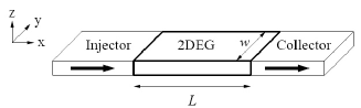
Figure 1 shows a schematic drawing of a SFET with finite width . Within the 2DEG in the -plane, the effective Hamiltonian of electrons reads
| (1) |
where is the momentum operator within the 2DEG, is the transverse confinement potential with for and otherwise. Here is the Pauli spin operator, and a unit vector perpendicular to the 2DEG.
In order to focus on the issue of the multichannel transport, we assume situations where effects of other practical problems are minimized; scattering by impurities and phonons is ignored in and ideal spin injection and detection are assumed. To be specific, an electron in the injector and collector is assumed to be subject to the following Hamiltonian,
| (2) |
where is the effective exchange energy in the injector/collector, is the Lande’s g-factor, and is the Bohr magneton. For sufficiently large (0), electrons in the injector and collector are 100% spin-polarized along the -direction. Note that with this choice of , the Fermi wavelength of -polarized electron within the injector/collector matches perfectly with that within the 2DEG when and thus the so-called conductance mismatch problem for the spin injection/detection does not appear for the 2DEG-injector(collector) interface. For nonzero , there is a weak mismatch in the Fermi wavelength but for the range of values examined below ( eVm), the conductance mismatch problem turns out to be a weak effect (see Appendix A for details).
II.1 Numerical conductance calculation
For the numerical conductance calculation of the multichannel SFETs, we use the tight-binding (TB) Hamiltonian Datta95Book ; Pareek02PRB , where amounts to the TB approximation of the Hamiltonian [Eq. (1)] for the 2DEG,
where is the annihilation operator of an electron at with spin along the -axis, is the lattice spacing used for the TB approximation, and and are related to the length and width of the 2DEG via and , respectively. With the choice and , Eq. (II.1) reduces to Eq. (1) in the limit . The TB Hamiltonians for the injector and collector are similarly given by
where . Note that the electron operators for do not appear in , since the injector/collector is assumed to be 100% spin polarized along -direction. The coupling Hamiltonian between the 2DEG and the injector/collector is given by
| (6) | |||||
Note that electrons whose spin is pointing along the -direction are not allowed to hop between the 2DEG and the injector(collector). Note also that the hopping parameter in is the same as that in . Thus when effects of (or ) on the Fermi wavelength is not significant, the conductance mismatch problem should be minimal (see Appendix A for detail), allowing ideal spin injection and detection.
The Landauer-Büttiker formalism is used for the numerical conductance calculation and the method in Ref. Anantram98PRB is used to evaluate matrix elements of related Greens’ functions. The following parameters are used; , where is the free electron mass, and the Fermi energy eV, which, in the absence of and , amounts to the Fermi wavelength A and the electron density of cm-2 in the 2DEG. For the TB approximation, we choose . Thus the hopping energy becomes eV.
Below the conductance is first evaluated in two windows of , (010) eVm and (4555) eVm. In various candidate systems for the SFET such as InGaAs/InAlAs Nitta97PRL , InAs/GaSb Luo90PRB , InGaAs/InP Engels97PRB , and InAs/AlSb Heida98PRB , typically falls within the first window. A recent calculation Silva03PRB also reported that for III-V quantum wires, is typically in this weak coupling regime. Search for systems with higher is in progress and effects of strong RSO coupling on the energy spectrum are addressed theoretically Moroz99PRB . For CdTe/HgTe/CdTe, for instance, values up to eVm has been reported Schultz96SST , which motivates the second window. For a SFET with relatively short , the conductance is evaluated in a much wider window of , (0100) eVm.
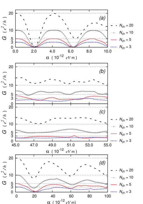
Figure 2 shows the evolution of the conductance as a function of for the SFET with 3, 5, 10, and 20 channels, respectively. For the range of examined below, the number of channels is related to the width of the 2DEG via the relation Datta95Book , where denotes the largest integer not exceeding . The length of the 2DEG is assumed to be m for (a) and (b), and m (m) for (c), and m for (d), respectively. In Fig. 2(a), the SFET is operated in the range from 0 to eVm. To estimate the spin precession angle, we use the formula . Though this formula is derived in the single-channel limit, it may still be useful to estimate the spin precession in multichannel SFETs. Then the average spin precession angle, estimated from the formula with the average eVm, is around , and the variation of the spin precession angle within the specified range is . Note that the SFET exhibits an almost ideal conductance modulation in the sense that the maximum of reaches almost and the minimum of reaches almost zero. The conductance modulation behavior becomes, however, less ideal with the increase of . For , for instance, Fig. 2(a) already shows some deviation from the ideal behavior. Figure 3(a) shows, as a function of , the ratio between and , where and are the maximum and minimum values of in the interval eVm eVm in Fig. 2(a). It clearly shows the decay of the ratio with .
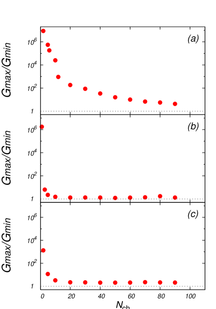
In Fig. 2(b) (again with m), the SFET is operated in the range eVm. Note that the width of the range is the same as that in Fig. 2(a). Since is larger than the values in Fig. 2(a), the spin precession angle will be larger. The average spin precession angle in this range, estimated from the formula with the average eVm, is around , about 10 times larger than in Fig. 2(a). On the other hand, the variation of the spin precession angle within the specified range is about , same as in Fig. 2(a). Note that the conductance modulation behavior is now much less ideal; the maximum and minimum of deviate considerably from and , respectively. Moreover the conductance oscillation with becomes somewhat irregular. Figures 3(b) shows, as a function of , the ratio between and for the SFET in Fig. 2(b). Here and are evaluated in the range eVm. Note that the decay of the ratio with increasing is much faster than that in Fig. 3(a). For small around 5, the ratio already drops to of order unity.
One intuitive explanation for the much less ideal behavior in Figs. 2(b) and 3(b), compared to Figs. 2(a) and 3(a), is fluctuations of the spin precession rates from channel to channel. For example, if the spin precession angles per length deviate from and the deviations fluctuate from channel to channel, the conductance modulation may become less ideal. To test this possibility, we examine a SFET with shorter since effects of the channel-to-channel fluctuation are expected to be weakened with decreasing . In Fig. 2(c), the length of the 2DEG is reduced to m (m). When the SFET is operated in the same range as in Fig. 2(b), the average spin precession is estimated to , which is about 44% smaller than that in Fig. 2(b), and the variation of the spin precession angle within the specified range is estimated to . Figure 2(c) shows that the conductance modulation is still far from ideal despite the 44% reduction in the average spin precession angle.
In Fig. 2(d), the length of the 2DEG is further reduced to m, one tenth of that in Fig. 2(a). When the SFET is operated in the range eVm, which is 10 times larger than in Fig. 2(a), the average spin precession angle and the variation of the angle within the specified range are exactly same as those in Fig. 2(a). Thus the situations in Figs. 2(a) and (d) are identical as far as the expression for the spin precession angle is concerned. The numerical calculation result in Fig. 2(d) indicates however that while the conductance modulation behavior is somewhat improved compared to those in Figs. 2(b) and (c), it is still less ideal than that in Fig. 2(a). Figure 3(c) shows the -dependence of the ratio for the situation in Fig. 2(d), where and are evaluated in the interval eV eVm. Note that the decay of the ratio is still much faster than in Fig. 3(a). This result leads one to conclude that the channel-to-channel fluctuations of the spin precession angles are not the main reason for the deviations from the ideal behavior.
II.2 Transport channels
In order to gain an insight into the numerical results in Figs. 2 and 3, it is useful to examine energy eigenfunctions and eigenenergies of [Eq. (1)]. Let denote a eigen wavefunction with energy . Due to the translational symmetry along the -direction within the 2DEG, it can be expressed as a superposition of four plane waves , where the plane wave is an eigenstate of in the absence of . Here all four wavevectors share the same longitudinal component and their transverse components are determined from the relation , which is the energy-dispersion relation in the absence of (see Fig. 4). The spinor is given by
| (7) |
where is defined by and . Then the four constraints from the boundary conditions fix the four coefficients , and the exact energy-dispersion relations and the eigen wavefunctions can be obtained. This procedure can be simplified further by using additional symmetries of . See Appendix B for further details on the symmetries, and Appendix C for the use of the symmetries for the evaluation of the exact energy-dispersion relation and the eigen wavefunctions.
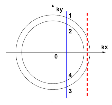
The red dotted lines in Fig. 5 denote the exact energy-dispersion relation for various situations. In comparison, the perturbatively obtained energy-dispersion relation (up to the second order in ) ,
| (8) |
is also depicted (blue solid lines) in Fig. 5. Here is the energy of the -th (=0,1,2,) excitation mode in the transverse direction, , and or . Equation (8) is obtained by treating the RSO coupling term in as a perturbation. Further details on the calculation of the energy dispersion relation via the second-order degenerate perturbation theory are given in Appendix D.
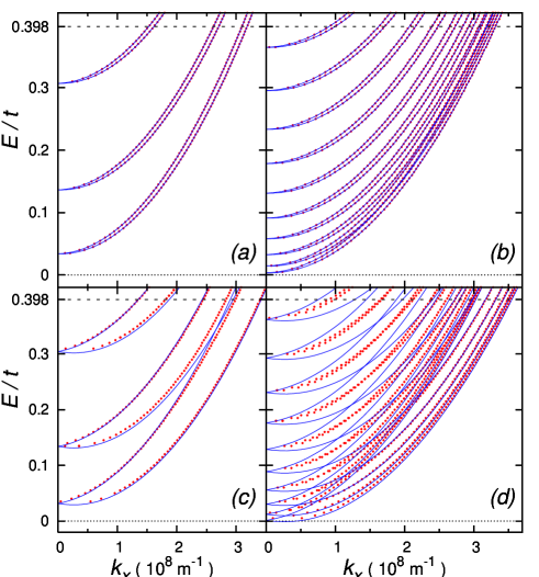
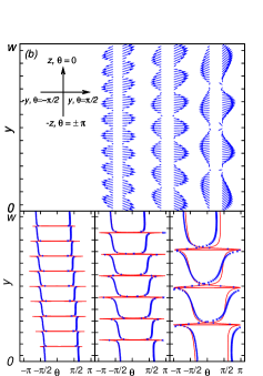
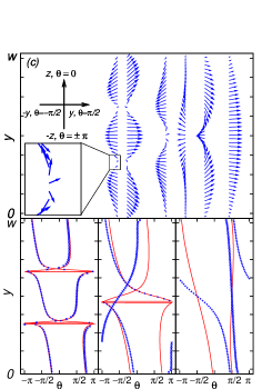
Figure 6 shows the local spin directions of the selected eigen wavefunctions at the Fermi level . The width and the RSO parameter for Figs. 6(a), (b), (c), and (d) are the same as those for Figs. 5(a), (b), (c), and (d), respectively. The local spin direction of an energy eigen wavefunction is independent of due to the translational symmetry of along the -direction. Also it can be shown that it is always perpendicular to the -axis and remains within the -plane since remains invariant under the symmetry operator (see Appendix B for further details), where is the time-reversal operator, is the mirror reflection operator with respect to the -plane in the orbital space, and is the rotation operator with respect to the -axis by the angle in the spin space. In each upper panel in Figs. 6(a), (b), (c), and (d), the arrows indicate the local spin direction as a function of for six selected exact eigen wavefunctions. The length of the arrows is proportional to , which is independent of . The six states in Figs. 6(a) and (c) are the six eigenstates in Figs. 5(a) and (c) at eV with increasing order of . On the other hand, the six states in Figs. 6(b) and (d) are the eigenstates in Figs. 5(b) and (d) at with the smallest, 2nd smallest, 7th smallest, 8th smallest, 13th smallest, and 14th smallest ’s (ordered according to the exact values) . The lower panels in Figs. 6(a), (b), (c), and (d) show the local spin angle as a function of , where is , 0, , when the local spin direction is pointing , , , axis, respectively. Here is related to the local spin direction via the spinor representation of a local spin direction that lies within the -plane, and , are the spinors pointing along the -directions. In each lower panel of Figs. 6(a), (b), (c), and (d), there are three subpanels, each of which shows the profiles of ’s for two selected energy eigen wavefunctions; ’s in the left/middle/right subpanel correspond to the two leftmost/central/rightmost spin textures in the upper panel. In the lower panels, blue dotted lines represent the exact results (see Appendix C for further details) and red solid lines are from the perturbatively obtained eigen wavefunctions calculated up to the second order in (see Appendix D for further details).
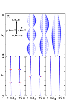
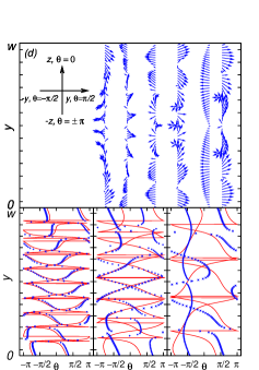
In Figs. 5 and 6, two representative values of , eVm [(a) and (b)] and eVm [(c) and (d)], are used. Figures 5(a) and 6(a) show the result for the smaller value and . Note that the perturbative result for the energy dispersion relation is in excellent agreement with the exact result. Equation (8) from the perturbation theory indicates that the energy dispersion relations for all channel are identical to each other up to the parallel shift by and remain parabolic. Moveover Fig. 6(a) indicates that the spin direction is essentially equal to the or -direction, same as in the ideal single-channel SFET. Thus the SFET for the situation in Fig. 5(a) and 6(a) should show an almost ideal behavior, which is indeed the case as demonstrated in Figs. 2(a) for . The channel-to-channel fluctuations of the spin precession angle should be negligible.
Figures 5(b) and 6(b) show the result for eVm and . The exact energy dispersion relations are again excellently fitted by the perturbative results [Eq. (8)], which are purely parabolic. The local spin directions, on the other hand, show noticeable deviations from the ideal -directions. The lower subpanels in Fig. 6(b) show that near the “nodal” points, where the length of the spin arrows in the upper panel of Fig. 6(b) almost vanishes, changes rapidly by , forming “phase-slip”-like structures. The phase-slip-like structure near the nodal points is more clearly visible in the magnified plot in the inset of Fig. 6(c). Superimposed over the phase-slip-like structures, there is also a gradual drift of with the increase of . To understand the origin of the deviations, the eigen wavefunctions are perturbatively evaluated (see Appendix D). Up to the first order in , the perturbative calculation for the reduced wavefunction [] results in
| (9) |
where and are defined in the same way as in Eq. (8), and for and for . Here the zeroth order reduced wavefunctions are and respectively, where . From these expressions, one obtains simple expressions for ,
| (10) | |||||
which has been reported previously Hausler01PRB . Note that while the zeroth order terms in are -independent constants, , corresponding to the ideal -directions, the first order terms in are proportional to , explaining the gradual drift of with . In order to gain an insight into the phase-slip-like structure, we next examine the second order corrections to . Since the first order correction in Eq. (9) identically vanishes at the nodal points () of , the second order corrections are the first nonvanishing terms near those nodal points. Moreover since is a topologically singular point for the local spin angle , even a small and smooth corrections to can result in a rapid change of by . The local spin angles evaluated from the second order perturbation theory are shown (red solid lines) in the lower subpanels in Fig. 6(b), indeed reproducing the phase-slip-like structure. The perturbative results are in reasonable agreement with the exact results. The expressions for the second order corrections to are rather lengthy [Eqs. (31) and (32)] and given in the Appendix D only. We remark that the gradual drift and the phase-slip-like structures are also present in Fig. 6(a), though they are much weaker. Since they can be explained within the perturbation theory, the strength of their effects is expected to depend on the magnitude of the small expansion parameter of the perturbation theory, which is according to Eqs. (9), (31), and (32). Then recalling that the product is about 0.28 for the 3 channel system and about 0.86 for the 10 channel system, the difference between Figs. 6(a) and (b) can be explained. This analysis also implies that the deviations of the local spin configuration from the ideal spin directions will be magnified with the increase of . Since these deviation will certainly cause the conductance to deviate from the ideal SFET behavior based on the ideal spin directions, this analysis also provides an explanation for the initial decay of the conductance modulation ratio with the increase of demonstrated in Figs. 2(a) and 3(a).
Figures 5(c) and 6(c) show the result for the larger eVm and with the product 1.7, which is about two times larger than in Figs. 5(b) and 6(b). Figure 5(c) shows that now some energy dispersion relations noticeably deviate from the parabolic behaviors. While many subbands are still well fitted by the parabolic perturbative results, the two subbands, which are predicted by the perturbation calculation to cross near m-1, are affected by the subband mixing and the avoided crossing structure appears, which goes beyond the perturbation calculation in Appendix D. At , the states with the second and third largest ’s are affected by the avoided crossing and their dispersions deviate from the parabolic dependence, modifying the spin precession rates of the involved channels as demonstrated recently Egues03APL . The avoided crossing also affects the local spin angle. For those two states affected by the avoided crossing, the exact local spin angle profiles deviate considerably from the perturbative results [lower subpanels of Fig. 6(c)]. For the other four states, the exact local spin profiles are reasonably well fitted by the perturbative results. Note that the gradual drift of and the phase-slip-like structure are more evident than in Fig. 6(b), which is natural in view of the about two-fold increase of the product . Based on this analysis, we attribute the reduced conductance modulation ratio in Figs. 2(b) and 3(b) (even for small such as 3) jointly to the perturbative spin configuration change and the avoided crossing. We remark that the avoided crossing in fact occurs in Fig. 5(b) as well, though not clearly visible in the figure since its effects on the energy dispersions are restricted to rather narrow ranges of . Furthermore the avoided crossing appears far below , so that its effects on the conductance is negligible.
Figures 5(d) and 6(d) show the result for eVm and with 5.2. It turns out that most subbands are affected by the avoided crossing and the agreement between the perturbative and exact dispersion relations is poor. The agreement between the perturbative and exact spin configuration is again poor for many states at . The abundance of the avoided crossing explains the strongly suppressed conductance modulation ratio of the SFET operated with larger [Figs. 3(b) and (c)].
III Coherent SFET
The electronic coherence may give rise to interesting effects in mesoscopic systems Datta95Book ; Seba01PRL . For a single channel system, it has been predicted Schapers01PRB ; Mireles02EL ; Larsen02PRB ; Lee05PRB that due to the electron coherence, the conductance behavior of a SFET deviates from the conventional sinusoidal dependence . In this section, we investigate effects of the coherence on multichannel SFETs. In particular, we focus on situations with and eVm since for larger and , the coherence effects will be mixed with other effects such as nonideal spin configuration and avoided crossing, making clear identification of the coherence effects difficult.
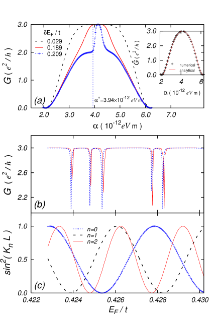
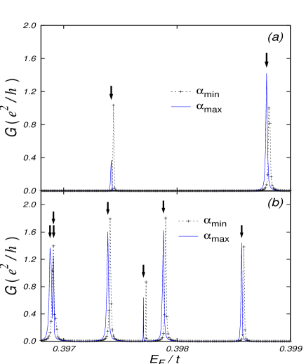
Hints of the coherence effects appear already at Fig. 2(a). A close look reveals the deviation of the line profile from the sinusoidal behavior . The evolution of with the variation of the Fermi energy illustrates the deviation more clearly. Figure 7(a) shows of a SFET with for a number of ’s. ’s in Fig. 7(a) are measured with respect to the reference energy 0.103 eV0.398. While is not sensitive to near the conductance maximum (near eVm) and the minimum (near eVm and eVm), the profiles of including the full-width-at-half-maximum (FWHM) exhibit considerable dependence on . Moreover near certain special ’s such as , shows a nested peak structure, where a small peak appears on top of a bigger background peak. These results are in clear contrast to the result in Ref. Mireles01PRB , which reports the absence of the -dependence when . While our conductance calculation takes into account all three parts (2DEG, injector, and collector) quantum mechanically, only the 2DEG is quantum mechanically treated in Ref. Mireles01PRB . We believe that this is responsible for the difference.
In order to examine the connection between the electronic coherence and the nested peak structure, we first recall that in a single channel SFET, the conductance calculation Lee05PRB , which takes into account the electronic coherence, results in
| (11) |
where , , and and are the two longitudinal wavevectors at . The deviation of Eq. (11) from the sinusoidal behavior arises from the fact that the injector and collector behave as reflecting walls for the electron spin component antiparallel to the favored spin direction in the injector and collector. Thus the unfavored spin component may be reflected many times by the ideal injector and collector until it acquires, via the spin precession by the RSO coupling, some component parallel to the favored spin component and is transmitted to the injector or collector. Thus in addition to the direct contribution that does not undergo any reflection, there are -th order contributions to the electron transmission that undergo the reflection times until being transmitted to the collector. In this sense, the coherent SFET is analogous (though not identical) to the Fabry-Perot interferometer. It is straightforward to verify that the amplitude of the -th contribution is smaller than that of the -th contribution by the factor for and by the factor for . Here the zeroth () contribution denotes the direct contribution. Note that the interference between the direct contribution and the multiply reflected contributions is destructive (constructive) when the phase is (). This explains the factor in Eq. (11), which predicts the suppression (enhancement) of the FWHM of the profile when (1). Since depends on , this dependence also implies the dependence. To examine the coherence effects in a multichannel SFET, we use an intuitive generalization of Eq. (11) to a multichannel system;
| (12) |
where , and is the longitudinal wavevector at for the subband (see Fig. 5). Equation (12) is expected to be a reasonable approximation when the inter-channel mixing is weak and each channel is close to an ideal 1D channel, which are indeed the case for eVm and as demonstrated in Sec. II. In Fig. 7(b), the prediction of Eq. (12) (blue dashed line) for as a function of is compared with the numerical TB conductance result (red solid line), where eVm [vertical dashed line in Fig. 7(a)]. Since is close to the position where the conductance retains its maximal value , the dips in imply the formation of the nested peak structure. To compare with the TB calculation result, and in Eq. (12) are expressed in terms of the TB parameters. To evaluate , we use the relation , which amounts to the TB approximation of Eq. (8). Here . To evaluate , we use , where is an ad hoc fitting parameter much smaller than . Note that Eq. (12) produces dips (blue dashed line) and moreover the dip positions predicted by Eq. (12) are in good agreement with the TB conductance calculation result (red solid line). Thus Eq. (12) reproduces the nested peak structure. We remark that when is used, the dips in the blue dashed line shift to the right by only (not shown), not affecting the agreement significantly.
The agreement provides a simple insight into the origin of the nested peak structure. A key observation is that while all ’s in Eq. (12) produce the conductance peaks at the same , the peak widths may fluctuate considerably from channel to channel. The channel-to-channel peak width fluctuation arises from the dependence of the peak width on . In particular when , the peak produced by becomes very narrow. Thus when is close to zero for one particular , one very narrow peak for that particular is superposed with the other broad peaks, generating the nested peak structure. Figure 7(c) plots ’s as a function of . Note that whenever one of vanishes, a dip appears in Fig. 7(b). We remark that though the nested peak structure is illustrated mainly for , it appears for higher as well. An example for is visible in Fig. 2(a) near eVm. For sufficiently large , however, the nested peak structure is expected to vanish. The nested peak structure was not found in a two-dimensional coherent SFET Matsuyama02PRB , which amounts to the limit.
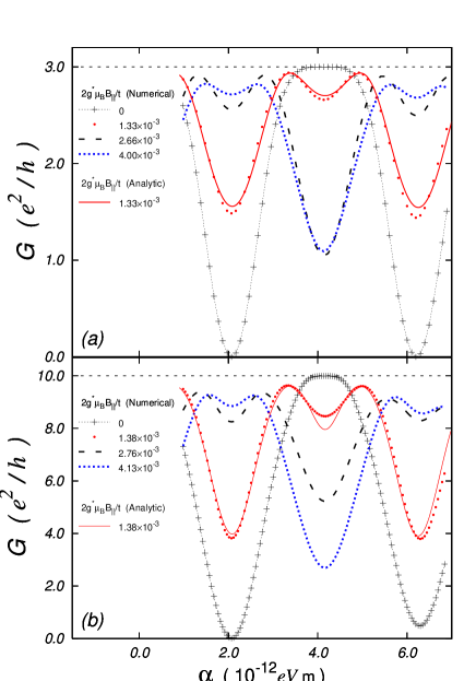
The electronic coherence can give rise to another interesting effect when an external magnetic field is applied, providing an additional source of the spin precession. Here we consider applied along the -axis, so that the spin precession axis by is parallel to that due to the RSO coupling in the ideal 1D situation. The spin precessions by and the RSO coupling differ in one crucial respect; When the electron reverses its motion, the direction of the spin precession by the RSO coupling is reversed while that of the spin precession by is not. For a single channel SFET, it is illustrated Lee05PRB that this difference, combined with the coherent Fabry-Perot-like interference, gives rise to the splitting of the conductance peaks upon the application of . Figure 8 shows that the magnetic-field-induced peak splitting occurs also for multichannel SFETs. The numerical TB conductance calculation results are compared with the expression,
| (13) |
which is an intuitive extension of the single channel formula in Ref. Lee05PRB . Here denotes the spin precession angle due to . For weak fields, it is given by , where is the effective Lande- factor, is the Bohr magneton, and is the group velocity of electrons with energy in the -th channel Kn-comment . Note that the predictions of Eq. (13) are in reasonable agreement with the numerical TB results both for and 10.
IV Discussion
An ideal spin injector/collector has been assumed in the preceding sections in order to focus on the multichannel effects. For a certain material to be an ideal spin injector/collector, (i) its spin polarization should be 100% and (ii) its effective mass and Fermi wavelength should match those for the 2DEG. While the condition (i) is satisfied in the so-called half-metals Groot83PRL and the condition (ii) may be satisfied in ferromagnetic semiconductors or diluted magnetic semiconductors Ohno98Science , we are not aware of any material that satisfies the both conditions. In Sec. IV.1, we thus address briefly effects of a nonideal spin injector/collector on the multichannel SFET.
IV.1 Nonideal spin injector/collector
One of most explored and representative choices for a spin injector/collector is conventional metallic ferromagnets, whose spin polarization can be as high as . Use of conventional metallic ferromagnets requires a special care. Recent theories Rashba00PRB proposed that the spin injecton/detection rate can be greatly improved by introducing a thin insulator between a conventional ferromagnet and the 2DEG while without the insulator, the spin injection/detection rate was demonstrated Filip00PRB to be below 1% due to the so-called conductance mismatch problem Schmidt00PRB . The physics behind the insulator “prescription” for the conductance mismatch problem is that the tunneling through the insulating barrier becomes spin-dependent Rashba00PRB in the ferromagnet-insulator-2DEG geometry even though the insulator is nonmagnetic. Subsequent experiments Motsnyi03PRB using oxide insulating barriers have reported the enhanced spin polarization of 2-30% at room temperatures. Schottky tunnel barriers were also demonstrated to be effective and the spin polarization of 2-30% has been reported Zhu01PRL at low temperatures.
Here we calculate numerically the conductance of the multichannel SFET equipped with the nonideal spin injector/collector that consists of a conventional metallic ferromagnet-thin insulator-2DEG hybrid structure.
One possible way to model the spin-dependent tunneling in the ferromagnet-insulator-2DEG structure is to explicitly take into account all three materials, ferromagnet, insulator, and 2DEG (Appendix E). This approach is however too demanding for numerical calculations since the Fermi wavelength in the ferromagnet is about two orders of magnitude smaller than that in the 2DEG. We thus adopt a simplified phenomenological description, where all effects of the ferromagnet (including not only its spin-dependent density of states but also the effective mass and the Fermi wavelength differences from those of the 2DEG) are taken into account by phenomenological spin-dependent hopping parameters for the tunneling through the insulator. To be specific, the TB Hamiltonian [Eq. (6)] for the coupling between the 2DEG and the injector/collector is modified as follows:
| (14) | |||||
where is a spin-dependent hopping parameter that takes into account not only the spin-dependent tunneling through the insulator but also other effects from the effective mass and the Fermi wavelength differences between the ferromagnet and the 2DEG. Since all effects of the ferromagnet are already taken into account in [Eq. (14)], the injector/collector may be modelled as a nonmagnetic semiconducting lead, which can be described by modifying [Eqs. (II.1) and (II.1)] so that similar contributions for are also included. Although this description adopts a considerably simplified picture of the real system, it is still expected to capture the main physics of the spin injection/detection since, as demonstrated in Refs. Rashba00PRB and Appendix E, the spin-dependent tunneling through the insulator is the main source of the sizable spin injection/detection rate () while the bulk properties of the ferromagnet generate much weaker contributions only. We choose the value of to be for and for , respectively. The resulting spin polarization of the injected current estimated by is then 30%, which is similar to the values reported in experiments Motsnyi03PRB .
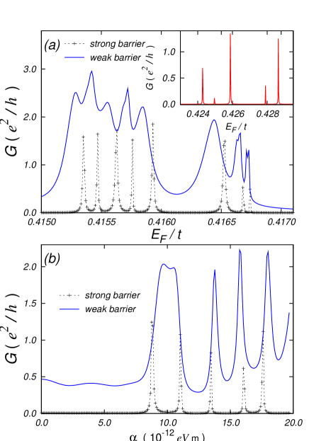
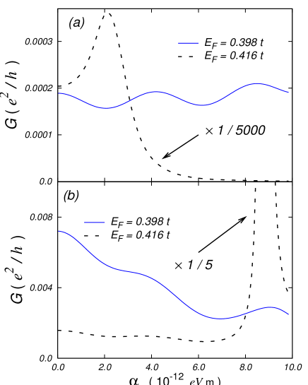
For and [solid line in Fig. 9(a)], clearly shows the modulation by though the value of is considerably reduced below due to the insulating barriers and the ratio is also suppressed due to the reduced spin injection/detection rate of 30%. Thus for this particular situation, shows rather expected behaviors. For other situations, somewhat unexpected behaviors also appear. For and [dashed line in Fig. 9(a)], the “periodic” modulation disappears and instead a large peak appears at eVm with the maximum conductance of (the peak height is scaled down by the factor of 5000 to fit in the vertical scale of the graph). For and [dashed line in Fig. 9(b)], a large peak (near eVm) coexists with the modulation in the lower range. For and [solid line in Fig. 9(b)], the modulation is superimposed on a background slope.
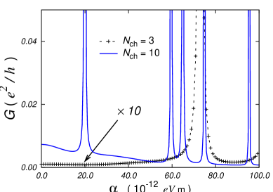
To investigate how frequently such peaks appear, is evaluated as a function of for two representative values of , eVm and eVm, which correspond to the positions of the local minimum and maximum of at for . For [Fig. 10(a)], two peaks appear in the depicted range and for [Fig. 10(b)], seven peaks appear. Thus the occurrence of the peaks becomes more frequent with the increase of . The calculation for =3, 10, and 20 over a much wider range of (, not shown) verifies this trend. Note that the peak positions for and are somewhat different, implying that the peak positions shift with . Considering that the peak heights () are three or four orders of magnitudes larger than the modulation amplitudes in Fig. 9, even tails of the peaks can be large “perturbations” to the modulation and thus the -dependence of the peak positions, though weak, can affect the modulation considerably. As remarked above, this perturbation appears more frequently for larger .
To find the origin of the large peaks, their dependence on the strengths of the hopping parameters is examined. As demonstrated in Fig. 11, the peak widths for the large hopping parameters (, ) are larger than those for the small hopping parameters (, ). This difference in the peak widths implies that the large peaks are resonances due to the electron confinement effects of the insulators. Then at the energies where the resonances appear, the phase acquired by electrons during their motion from the injector to the collector should be an integer multiple of . Interestingly this condition is the same as the condition for the occurrence of the nested peak structure in Sec. III. The comparison between the inset in Fig. 11(a) for the large resonance peaks and Fig. 7(b) for the nested peaks indeed verifies this relation between the two phenomena. Recalling that the inter-channel coupling is weak for and eVm, the correlation between the number of resonance peaks and can also be explained easily since each channel separately gives rise to resonances.
Lastly we examine effects of the nonideal spin injector/collector on a shorter SFET. Figure 12 shows the conductance evolution for a SFET with relatively short m in a much wider window of , eVm. Again large resonance peaks appear, distorting the spin-orbit-coupling-induced modulation of the conductance considerably. We remark that the decrease of clearly enhances the spacing of the resonances both in the vs. plot and in the vs. plot (not shown). However considering that the decrease of also widens the minimum size of the “window” for the observation of the spin-orbit-coupling-induced modulation of and that the change of simply “parallel” shifts the resonance positions in the vs. plot, reducing does not appear to significantly facilitate the observation of the spin-orbit-coupling-induced modulation of .
IV.2 Scattering effects
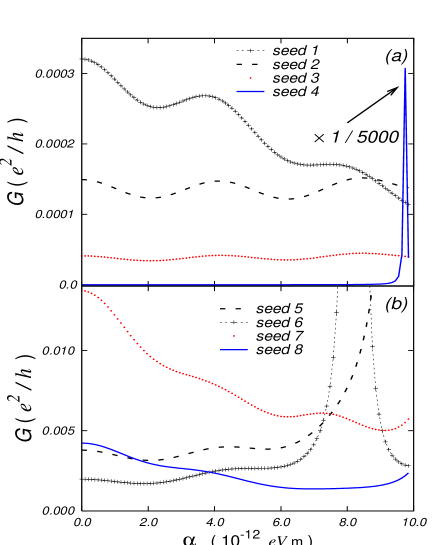
Another practical problem ignored in the preceding sections is the scattering effects. Scattering by impurities, which are isotropic, short-ranged, and spin-independent, can be modelled by using the TB Hamiltonian of the impurity potential given by , where is a random variable whose value is uniformly distributed in the range . We investigate briefly the scattering effects in a weakly diffusive regime; is chosen in such a way that the mean free path is . The nonideal spin injector/collector is again assumed and , are used. Figure 13 shows as a function of for various realizations of the random potential . For all realizations, is the same. Note that for certain realizations, the spin-orbit-coupling-induced modulation of is clearly visible while for other realizations, the modulations is strongly distorted by the resonance peaks. This difference is due to the fact that the positions of the resonances depend on details of the spatial profile of the random potential . A similar result is obtained for a nonballistic single-channel SFET Cahay03Cond . The results in Fig. 13 also imply that the conductance of a nonballistic multichannel SFET equipped with the nonideal spin injector/collector may show considerable sample-to-sample fluctuations. Recalling that there are more resonance peaks for larger , the sample-to-sample fluctuations are expected to be more significant for larger . More systematic studies about nonballistic multichannel SFETs with the nonideal injector/collector are necessary.
V conclusion
The issue of multichannel effects were addressed. Via the numerical conductance calculation using the tight-binding approximation, it has been demonstrated that the conductance modulation becomes less ideal with the increase of the channel number . For the ideal spin injector/collector, the conductance modulation ratio as a function of (from a few to 90) has been examined for the RSO coupling parameter eVm and for the larger eVm. It has been found that the decay of the modulation ratio with is considerably faster for the larger . Through the study of the energy dispersion relations and the spin configurations of eigenstates, it has been revealed that with the increase of and , the spin configuration deviates further from the ideal 1D configuration due to the formation of the phase-slip-like structure and the gradual drift of the spin angle, and that the energy dispersion deviates further from the ideal quadratic dispersion since the avoided crossing distorts the dispersion in a wider range of the longitudinal wavevectors. It turns out that those deviations are rather small when while they become significant when . Thus this result provides insights to the regime , where the inter-channel coupling is expected to be significant Datta90APL ; Mireles01PRB . Effects of the electronic coherence in the multichannel regime were also examined and we have found the nested peak structure, which was attributed to the coherent Fabry-Perot-like interference in the multichannel regime. We have also verified that the magnetic field-induced peak splitting, reported previously Lee05PRB for a single-channel SFET, persists in the multichannel regime. For the nonideal spin injector/collector that consists of a conventional metallic ferromagnet-thin insulator-2DEG hybrid structure, it has been found that large resonance peaks due to the electron confinement by the insulators may strongly distort the spin-orbit-coupling-induced modulation of the conductance. When the 2DEG becomes weakly diffusive, the conductance modulation signal shows considerable sample-to-sample fluctuations.
Acknowledgements.
We acknowledge H.-S. Sim, Hyowon Park, Woojoo Sim, and J.-H. Kim for their help on numerical calculations. This work was supported by the SRC/ERC program (Grant No. R11-2000-071) and the Basis Research Program (Grant No. R01-2005-000-10352-0) of MOST/KOSEF, by the POSTECH Core Research Program, and by the Korea Research Foundation Grant (Grant No. KRF-2005-070-C00055 and BK21 program) funded by the Korean Government (MOEHRD).Appendix A Ideal injector and collector
As a test of the ideal spin injector, we calculate the electron transmission probability through the injector-2DEG interface for an electron incident from the injector side with the incident momentum and its spin pointing along the favored direction, -axis. The model Hamiltonian of the injector-2DEG hybrid system reads , where is the Heaviside step function. Since we are mainly interested in interface effects on the spin injection, the confinement potential in and is ignored below. For , is since and are identical for the electron with its spin pointing along the -axis. For nonzero , will deviate from one.
The evaluation of is straightforward. Recalling that the eigenspin direction in the 2DEG differs from -direction and that the injected electron wave is thus a superposition of two plane waves with different spin directions, one needs to match properly the superposition with the electron state in the injector. The result is shown in Fig. 14 for the three incident angles , , and , where . Note that regardless of , remains close to 1 up to considerably large , eVm. Note also that and (), transmission probabilities into each of the two plane wave states in the 2DEG, remain close to their values and in the limit , indicating that the spin of the injected electron points along the -direction right after the injection. Figure 14 thus verifies the ideal spin injector. The ideal spin collector can be verified in a similar way.
Appendix B Symmetry analysis
Symmetries often facilitate the analysis of a system and provide useful information Zhai05PRL . Since [Eq. (1)] is invariant under the translation along the -axis, an energy eigenfunction can be written as where is the spin component along the -direction, Pauli spin-up state and spin-down state.
also commutes with two other symmetry operators and , where is the time-reversal operator, is the mirror reflection operator with respect to the -plane in the orbital space, and is the rotation operator with respect to the -axis by the angle in the spin space. To examine implications of these symmetry operators, it is convenient to use the representation , and , where is the complex-conjugation operator in the real space representation with the -axis as the spin quantization axis. Application of on results in . Since , the resulting state should also be an energy eigenfunction with the energy eigenvalue same as that for . Then by comparing with , one finds that without loss of generality, may be chosen to be real and may be chosen to be imaginary. Recalling the spinor representation for the spin with the polar angle and the azimuthal angle , one finds that for the energy eigenfunctions is and that the spin direction of the energy eigenfunctions always lies within the -plane.
When the confining potential is symmetric , which is the case for the hard wall confinement potential, allows another symmetry operation , where is the mirror reflection operator with respect to the plane in the orbital space and is the rotation operator with respect to the -axis by the angle in the spin space. Since , possible eigenvalues of are and , and the energy eigenfunctions can be classified into even and odd parity states accordingly. For notational convenience, we choose for even parity states and for odd parity states. At the special point , plays no role and the parity becomes identical to the eigenvalue of . Thus at , the spin of the even parity states points towards -direction (, ) and the spin of odd parity states points towards -direction (, ). For , the spin in general deviates from -direction. But due to the parity constraint, the spin directions at and are correlated; .
Appendix C Hard wall confinement : Exact results
An exact energy eigenstate of [Eq. (1)] with energy can be expressed as a linear superposition of plane waves as follows,
| (15) |
where the plane wave is an energy eigenfunction of in the absence of the confinement potential [], , , and ’s are four solutions of (see Fig. 4). When all four solutions are real (denoted by the blue solid line in Fig. 4), one may take and . But in certain situations (denoted by the red dashed line in Fig. 4), only two solutions are real and the other two remaining solutions are pure imaginary. We remark that in order to obtain a complete energy spectrum, one should consider such situations as well. In such situations, one may take for the two real solutions and for the other two purely imaginary solutions. The procedure described below applies to both situations (blue solid line and red dashed line) denoted in Fig. 4. For the spinors and , we choose the representation,
| (16) |
and
| (17) |
For the spinors and , we choose their representation in such a way that the plane waves ’s satisfy the relations, and , which is possible since is a symmetry operation of the system.
The four coefficients ’s in Eq. (15) are fixed by the hard-wall boundary conditions, , which lead to a secular equation for a matrix. Solving this equation is facilitated by the symmetry operation . Since has only two eigenvalues, and , the eigenstates can be classified into even and odd parity states. For an even parity state, one may choose and , and for an odd parity state, one may choose and . Thus the secular equation for the matrix is block-diagonalized into two matrices, one for even parity states and the other for odd parity states. By solving the two matrices separately, one obtains the eigenenergy and the corresponding eigenstate for even and odd parity states. Figure 5 shows the energy dispersion for various combinations of and . Figure 6 shows the spin profiles of selected eigenstates.
Appendix D Perturbation theory
Although the exact eigen wavefunctions and energy-dispersion relations are readily available, perturbation theory calculations are still useful in order to gain insights into the -dependence of eigen transport channels. Below we treat the RSO coupling as a perturbation and examine its effects on eigen transport channels. Since the longitudinal momentum is an exact quantum number of in Eq. (1), one may work with the reduced Hamiltonian that acts on the transverse part of the original wavefunction . Here the unperturbed Hamiltonian and the perturbation are given by
| (18) |
where is the identity operator acting on spin.
In the zeroth order in , each energy eigenvalue of is doubly degenerate with where is the energy of the -th (=0,1,2,) excitation mode in the transverse motion and . The corresponding eigenfunctions are and respectively, where , and , are the spinors pointing along the -directions.
Corrections to the eigenenergies can be obtained easily. The first order corrections to (1,2) are given by the representation of within the two-dimensional degenerate subspace:
| (19) |
Thus one obtains the first order energy correction . Note that since the matrix of Eq. (19) is diagonal, and are the proper zeroth order eigenfunctions in view of the degenerate perturbation theory. The second order energy corrections are given by
| (20) |
where the projection operator is defined by . By using the identity and the relation , Eq. (20) can be written as
| (21) |
which reduces further to
| (22) |
with the help of the identities and . Thus up to the second order in , the energy dispersion relation is given by
| (23) |
The result is shown in Fig. 5. Here we remark that although Eq. (23) is derived for the hard-wall confinement potential, the first- and second-order corrections to the eigenenergy are independent of ; its change alters only the zeroth order contribution . A similar result for a harmonic confinement has been reported previously Serra05PRB .
Next we examine corrections to energy eigenstates. According to the degenerate perturbation theory, the first order corrections , where and , are given by
| (24) |
and
| (25) |
where for and for . Both Eqs. (24) and (25) can be considerably simplified. With the help of the identities , , and , one finds
| (26) |
| (27) |
where . Then up to the first order in , the eigen wavefunctions are given by
| (28) |
We remark that although Eq. (28) is derived for the hard wall confinement, it holds for other confinement potentials as well when is evaluated for the new . The second order correction is given by
| (29) | |||||
| (30) | |||||
With the help of similar identities, one finds
| (31) | |||||
| (32) |
where . We remark that these expressions for the second correction are again independent of the choice of .
These expressions contain the information on the local spin direction. Since the Hamiltonian is invariant under the transformation , the local spin direction is always perpendicular to the -axis as demonstrated in Appendix B and it can be parameterized by a single angle within the plane; The local spin direction is pointing , , , and axis when is , , , and , respectively. By using the perturbatively obtained wavefunctions, the angle can be expanded as a power series of , , where the zeroth and the first order contributions are
| (33) |
and
| (34) |
A similar result has been reported previously Hausler01PRB . Note that the first order contributions change linearly with , explaining the gradual drift in Fig. 6. Note also that despite the -dependence of the local spin directions of and remain antiparallel to each other [] at every position up to the first order in since up to the first order in . The second order contribution can be also obtained (expressions not shown) from the perturbative expressions for and it turns out that when ’s are taken into account, the local spin directions of and are not antiparallel to each other any more. Solid lines in Fig. 6 show calculated from the perturbative expressions for , where it is clear that the deviation of from becomes more evident for larger . The second order contribution is responsible for the phase-slip-like structure in Fig. 6.
Appendix E A nonideal spin injector

Here we consider the spin injection from a nonideal injector, which consists of a conventional metallic ferromagnet(F)-insulator(I)-2DEG heterostructure. The differences of the effective masses, the densities of states, and the Fermi wavelengths between the F and the 2DEG are taken into account and the electron transport within the F and the 2DEG is assumed to be ballistic. It has been reported Teresa99PRL that the detailed structure of the spin dependent density of states within the insulator can influence the spin polarization of the injected electron. In this paper, however, we ignore such details for simplicity and model the insulator by a -function potential , where denotes the tunnel contact parameter Blonder82PRB ; Hu01PRL . The model Hamiltonian of the F-I-2DEG hybrid system reads , where has the form . Here, represents the exchange interaction of the Stoner model in the F, and denotes the difference between the bottoms of the energy bands for the F and 2DEG. Below we ignore the confinement potential and focus on the case of the normal incidence () from the F since the Fermi wave vector in the F is much larger than that of the 2DEG Matsuyama02PRB and thus the normally incident electrons constitute a major portion of the injected electrons. We choose the value of the Fermi energy and the exchange interaction of the F to be eV and eV, respectively, and set the Fermi energy of the 2DEG to eV. Thus eV. Figure 15 shows the spin polarization of the injected currents as a function of the tunnel contact parameter , where is a measure of the spin polarization along the -direction and is defined by . Here represents the electron transmission probability through the F-I-2DEG structure for an incident electron with the spin . Note that while is only a few percent in the absence of , it grows close to 30%. This demonstrates clearly that the spin-dependent tunneling over the insulator barrier is the main source of the spin polarization of the injected current while the bulk properties of the F are rather irrelevant factors for the spin polarization of the injected current. This observation, which is in agreement with Refs. Rashba00PRB ; Hu01PRL , justifies the simplified description in Sec. IV.1 of the F-I-2DEG structure, where the differences between the two bulks (F and 2DEG) are ignored while the spin-dependent tunneling over the I is taken into account.
References
- (1) Yu. A. Bychkov and E. I. Rashba, J. Phys. C 17, 6039 (1984); JETP Lett. 39, 78 (1984).
- (2) J. Nitta, T. Akazaki, H. Takayanagi, and T. Enoki, Phys. Rev. Lett. 78, 1335 (1997); T. Koga, J. Nitta, T. Akazaki, and H. Takayanagi, Phys. Rev. Lett. 89, 046801 (2002).
- (3) For a review, see I. Žutic̀, J. Fabian and S. Das Sarma, Rev. Mod. Phys. 76, 323 (2004).
- (4) S. Datta and B. Das, Appl. Phys. Lett. 56, 665 (1990).
- (5) A. T. Filip, B. H. Hoving, F. J. Jedema, B. J. van Wees, B. Dutta, and S. Borghs, Phys. Rev. B 62, 9996 (2000).
- (6) G. Schmidt, D. Ferrand, L. W. Molenkamp, A. T. Filip, and B. J. van Wees, Phys. Rev. B 62, R4790 (2000).
- (7) A. Bournel, P. Dollfus, S. Galdin, F.-X. Musalem and P. Hesto, Solid State Commun. 104, 85 (1997); A. Bournel, P. Dollfus, P. Bruno, and P. Hesto, Eur. Phys. J. AP 4, 1 (1998);
- (8) A. A. Kiselev and K. W. Kim, Phys. Rev. B 61, 13115 (2000); Phys. Status Solidi (b) 221, 491 (2000).
- (9) M. Cahay and S. Bandyopadhyay, Phys. Rev. B 69, 045303 (2004); A. G. Mal’shukov and K. A. Chao, Phys. Rev. B 61, R2413 (2000); S. Pramanik, S. Bandyopadhyay, and M. Cahay, Phys. Rev. B 68, 075313 (2003); Appl. Phys. Lett. 84, 266 (2004); J. Schliemann, J. C. Egues, and D. Loss, Phys. Rev. Lett. 90, 146801 (2003); E. Shafir, M. Shen, and S. Saikin, Phys. Rev. B 70, R241302 (2004); B. K. Nikolić and S. Souma, Phys. Rev. B 71, 195328 (2005).
- (10) S. Bandyopadhyay and M. Cahay, Appl. Phys. Lett. 85, 1433 (2004); S. Pramanik, S. Bandyopadhyay, and M. Cahay, IEEE Trans. Nanotechnol. 4, 2 (2005).
- (11) J. Luo, H. Munekata, F. F. Fang, and P. J. Stiles, Phys. Rev. B 41, 7685 (1990).
- (12) G. Engels, J. Lange, Th. Schäpers, and H. Lüth, Phys. Rev. B 55, R1958 (1997).
- (13) J. P. Heida, B. J. van Wees, J. J. Kuipers, T. M. Klapwijk, and G. Borghs, Phys. Rev. B 57, 11911 (1998).
- (14) M. Schultz, F. Heinrichs, U. Merkt, T. Colin, T. Skauli, and S. Lovold, Semicond. Sci. Technol. 11, 1168 (1996); J. Hong, J. Lee, S. Joo, K. Rhie, B. C. Lee, J. Lee, S. An, J. Kim, and K.-H. Shin, J. Korean Phys. Soc. 45, 197 (2004).
- (15) Th. Schäpers, J. Nitta, H. B. Heersche, and H. Takayanagi, Phys. Rev. B 64, 125314 (2001).
- (16) F. Mireles and G. Kirczenow, Europhys. Lett. 59, 107 (2002); Phys. Rev. B 66, 214415 (2002).
- (17) M. H. Larsen, A. M. Lunde, and K. Flensberg, Phys. Rev. B 66, 033304 (2002).
- (18) H.-W. Lee, S. Çalışkan and H. Park, Phys. Rev. B 72, 153305 (2005).
- (19) F. Mireles and G. Kirczenow, Phys. Rev. B 64, 024426 (2001).
- (20) S. Datta, Electronic transport in mesoscopic systems (Cambridge University Press, Cambridge, 1995).
- (21) See for instance Eq. (1) in T. P. Pareek and P. Bruno, Phys. Rev. B 65, 241305(R) (2002).
- (22) M. P. Anantram and T. R. Govindan, Phys. Rev. B 58, 4882 (1998).
- (23) E. A. de Andrada e Silva and G. C. La Rocca, Phys. Rev. B 67, 165318 (2003).
- (24) A. V. Moroz and C. H. W. Barnes, Phys. Rev. B 60, 14272 (1999); ibid. 61, R2464 (2000); M. Governale and U. Zülicke, Phys. Rev. B 66, 073311 (2002).
- (25) W. Häusler, Phys. Rev. B 63, 121310(R) (2001).
- (26) J. C. Egues, G. Burkard, and D. Loss, Appl. Phys. Lett. 82, 2658 (2003).
- (27) P. Šeba, P. Exner, K. N. Pichugin, A. Vyhnal, and P. Středa, Phys. Rev. Lett. 86, 1598 (2001).
- (28) For a single-channel SFET, it has been demonstrated Lee05PRB that the -dependence of the conductance profile is averaged out at temperatures sufficiently larger than , where is the Fermi velocity, and the high temperature expression is given by . Then a trivial generalization to a multichannel SFET is obtained by multiplying to the single-channel result.
- (29) T. Matsuyama, C.-M. Hu, D. Grundler, G. Meier, and U. Merkt, Phys. Rev. B 65, 155322 (2002).
- (30) In the evaluation of , smaller correction due to the RSO coupling is ignored. In the presence of , the definition of is altered to , where and are the longitudinal wavevectors at for the right and left moving electrons. In the absence of , this definition reduces to the definition right below Eq. (12).
- (31) R. A. de Groot, F. M. Mueller, P. G. van Engen, and K. H. J. Buschow, Phys. Rev. Lett. 50, 2024 (1983); K. P. Kämper, W. Schmitt, and G. Güntherodt, R. J. Gambino, and R. Ruf, Phys. Rev. Lett. 59, 2788 (1987); J. -H. Park, E. Vescovo, H. -J. Kim, C. Kwon, R. Ramesh, and T. Venkatesan, Nature (London) 392, 794 (1998).
- (32) H. Ohno, A. Shen, F. Matsukura, A. Oiwa, A. Endo, S. Katsumoto, and Y. Iye, Appl. Phys. Lett. 69, 363 (1996); H. Ohno, Science 281, 951 (1998); H. Ohno, J. Magn. Magn. Mater. 200, 110 (1999).
- (33) E. I. Rashba, Phys. Rev. B 62, R16267 (2000); D. L. Smith and R. N. Silver, Phys. Rev. B 64, 045323 (2001); A. Fert and H. Jaffres, Phys. Rev. B 64, 184420 (2001).
- (34) V. F. Motsnyi, P. Van Dorpe, W. Van Roy, E. Goovaerts, V. I. Safarov, G. Borghs, and J. De Boeck, Phys. Rev. B 68, 245319 (2003); X. Jiang, R. Wang, R. M. Shelby, R. M. Macfarlane, S. R. Bank, J. S. Harris, and S. S. P. Parkin, Phys. Rev. Lett. 94, 056601 (2005).
- (35) H. J. Zhu, M. Ramsteiner, H. Kostial, M. Wassermeier, H. -P. Schönherr, and K. H. Ploog, Phys. Rev. Lett. 87, 016601 (2001); A. T. Hanbicki, O. M. J. van ’t Erve, R. Magno, G. Kioseoglou, C. H. Li, B. T. Jonker, G. Itskos, R. Mallory, M. Yasar, and A. Petrou, Appl. Phys. Lett. 82, 4092 (2003).
- (36) M. Cahay and S. Bandyopadhyay, cond-mat/0306283.
- (37) F. Zhai and H. Q. Xu, Phys. Rev. Lett. 94, 246601 (2005).
- (38) L. Serra, D. Sánchez, and R. López, Phys. Rev. B 72, 235309 (2005).
- (39) J. M. De Teresa, A. Barthélémy, A. Fert, J. P. Contour, R. Lyonnet, F. Montaigne, P. Seneor, and A. Vaurès, Phys. Rev. Lett. 82, 4288 (1999).
- (40) G. E. Blonder, M. Tinkham, and T. M. Klapwijk, Phys. Rev. B 25, 4515 (1982).
- (41) C.-M. Hu and T. Matsuyama, Phys. Rev. Lett. 87, 066803 (2001).