Theoretical study of the conductance of ferromagnetic atomic-sized contacts
Abstract
Recently, different experiments on the transport through atomic-sized contacts made of ferromagnetic materials have produced contradictory results. In particular, several groups have reported the observation of half-integer conductance quantization, which requires having full spin polarization and perfectly conducting channels. Motivated by these surprising results, we have studied theoretically the conductance of ideal atomic contact geometries of the ferromagnetic 3 materials Fe, Co, and Ni using a realistic tight-binding model. Our analysis shows that in the absence of magnetic domains, the bands of these transition metals play a key role in the electrical conduction. In the contact regime this fact has the following important consequences for the three materials: (i) there are partially open conduction channels and therefore conductance quantization is not expected, (ii) the conductance of the last plateau is typically above , (iii) both spin species contribute to the transport and thus there is in general no full current polarization, and (iv) both the value of the conductance and the current polarization are very sensitive to the contact geometry and to disorder. In the tunneling regime we find that a strong current polarization can be achieved.
pacs:
73.63.Rt, 75.75.+aI Introduction
Metallic nanowires fabricated by means of scanning-tunneling microscope and break-junction techniques have turned out to be a unique playground to test basic concepts of electronic transport at the atomic scale.Agrait2003 Usually the conductance of these contacts is described by the Landauer formula , where the sum runs over all the available conduction channels, is the transmission for the th channel, and is the quantum of conductance. In the case of broken spin symmetry one should include a sum over spin and replace by in the previous formula. It has been shown that the number of channels in a one-atom contact is mainly determined by the number of valence orbitals of the central atom, and the transmission of each channel is fixed by the local atomic environment.Cuevas1998a ; Scheer1998 ; Cuevas1998b Thus, for instance, a one-atom contact of a monovalent metal such as Au sustains a single channel, while for -like metals such as Al or Pb one finds three channels due to the contribution of the orbitals. More importantly for the discussion in this work, in a transition metal such as Nb the contribution of the orbitals leads to five partially open channels.Cuevas1998a ; Scheer1998 ; Ludoph2000a
In the last years a lot of attention has been devoted to the experimental analysis of contacts of magnetic materials.Sirvent1996 ; Costa1997 ; Hansen1997 ; Ott1998 ; Oshima1998 ; Komori1999 ; Ono1999 ; Garcia1999 ; Ludoph2000b ; Viret2002 ; Elhoussine2002 ; Shimizu2002 ; Gillingham2002 ; Rodrigues2003 ; Gillingham2003a ; Gillingham2003b ; Untiedt2004 ; Gabureac2004 ; Yang2004 ; Costa2005 ; Bolotin2006a ; Keane2006 ; Bolotin2006b ; Viret2006 In particular, several groups have reported the observation of half-integer conductance quantization in the last stages of the breaking of nanowires.Elhoussine2002 ; Shimizu2002 ; Gillingham2002 ; Rodrigues2003 ; Gillingham2003a ; Gillingham2003b Moreover, some authors have shown that the conductance histograms are very sensitive to a magnetic field. For instance, Ono et al. Ono1999 reported that the peaks at and which are observed without magnetic field are joined by additional peaks near and for fields above 5 mT. These findings are rather surprising and challenge our present understanding of the transport properties of atomic-sized contacts. Half-integer conductance quantization would require to have fully spin-polarized contacts and conduction channels with perfect transparency. Neither of these properties are expected in the 3 ferromagnetic materials (Fe, Co, and Ni). In these transition metals both the majority spin and the minority spin electrons at the Fermi energy contribute to transport and, moreover, the partially occupied orbitals are expected to give rise to partially open channels. Finally, it is impossible in practice for a magnetic field to lift the spin degeneracy in a metallic contact. A field of 10 T produces a Zeeman splitting on the order of 1 meV, which is extremely small in comparison with the bandwidth of even a single-atom contact, this being at least on the order of several electronvolts.Cuevas1998a ; Cuevas1998b In this sense, in the absence of magnetic domains and magnetostriction, it is difficult to understand how an external magnetic field could significantly modify the conductance of an atomic contact.
More recently, Untiedt et al. Untiedt2004 measured the conductance for contacts of several magnetic metals (Fe, Co, and Ni) using break junctions at low temperatures and under cryogenic vacuum conditions. They reported the absence of fractional conductance quantization, even when a high magnetic field was applied, which agrees better with the picture described above. Several recent model calculations support these findings.Martin2001 ; Smogunov2002 ; Delin2003 ; Velev2004 ; Bagrets2004 ; Rocha2004 ; Jacob2005 ; Wierzbowska2005 ; Dalgleish2005 ; Jacob2006 These studies have convincingly shown that neither conductance quantization nor full spin polarization are to be expected in contacts of this kind.
In spite of the coherent picture that is emerging, one still misses in the literature a comparative analysis of the ferromagnetic 3 materials (Fe, Co, and Ni) that clarifies basic issues like which orbitals are relevant for the transport, the role of atomic disorder, or the dependence of the spin polarization of the current on the thickness of the contact. To fill this gap, we present in this work detailed calculations of the conductance of ferromagnetic atomic contacts of Fe, Co, and Ni. In our calculations we study ideal contact geometries using a realistic tight-binding model. We only consider situations where the contact region is a single magnetic domain. Our results indicate that for a few-atom contact of the three materials one can draw the following general conclusions: (i) there is no conductance quantization, mainly due to the partially open conduction channels of the minority spin electrons, (ii) the last plateau has typically a conductance above , (iii) the current is not fully spin-polarized and both spin species contribute to the transport, and (iv) both the value of the conductance and the current polarization are very sensitive to the contact geometry and disorder. The origin of all these findings can be traced back to the fact that the bands of these transition metals play a very important role in the electrical conduction. This is in contrast with other physical situations such as tunnel junctions or bulk systems. Finally, we find that in the tunnel regime, which is reached when the contacts are broken, the nature of the conduction changes qualitatively and almost fully spin-polarized currents are indeed possible.
The rest of the paper is organized as follows. In the following section we describe our tight-binding approach to compute the conductance of the ferromagnetic atomic contacts. Section III is devoted to the analysis of the results of the conductance of representative one-atom thick contacts of Fe, Co, and Ni. Moreover, we include in this section a discussion of the conductance in the tunnel regime. In Sec. IV we discuss the influence of atomic disorder on the conductance of single-atom contacts. Finally, in Sec. V we summarize and discuss the main results.
II Description of the theoretical model
Our goal is to compute the low-temperature linear conductance of atomic-sized contacts of the 3 ferromagnetic metals Fe, Co, and Ni. For this purpose, we use a tight-binding model based on the sophisticated parametrization introduced in Ref. [Mehl1996, ]. Such tight-binding models have been successful in the description of electron transport in metallic atomic contacts.Cuevas1998a ; Cuevas1998b ; Haefner2004 Our approach follows closely the one used in Refs. [Brandbyge1999, ; Dreher2005, ; Viljas2005, ], and we now proceed to describe it briefly.
In our approach the electronic structure of the atomic contacts is described in terms of the following tight-binding Hamiltonian written in a non-orthogonal basis
| (1) |
Here run over the atomic sites, denote the different atomic orbitals, and denotes the spin. Furthermore, for and are the spin-dependent on-site energies, and for the hopping elements, while for . In addition, we need the overlaps between the different orbitals, , which are spin-independent. We take all these parameters from the bulk parametrization of Ref. [Mehl1996, ], which is known to accurately reproduce the band structure and total energy of bulk ferromagnetic materials.Bacalis2001 Notice that in our model there is no mixing of the two spin species, which means that, in particular, we do not consider spin-orbit interaction. The atomic basis is formed by 9 orbitals (), which give rise to the main bands around the Fermi energy in Fe, Co, and Ni. It is important to emphasize that in this parametrization both the hopping elements and the overlaps are functions of the relative positions of the atoms, which allows us to study also geometrical disorder. These functions have a cut-off radius that encloses atoms well beyond the 10th nearest neighbors in a bulk geometry for Fe, Co, and Ni.
In order to compute the linear conductance, we apply a standard Green functions method [Cuevas1998a, ; Haefner2004, ; Brandbyge1999, ; Dreher2005, ; Viljas2005, ]. For this we divide the system into three parts, the left () and right () leads, and the central cluster () containing the constriction. In this way, the retarded central cluster Green functions, , are given by
| (2) |
Here and are the Hamiltonian and the overlap matrix of the central cluster, respectively, and are the self-energies, which contain the information of the electronic structure of the leads and their coupling to the central part of the contact. These self-energies can be expressed as
| (3) |
with a similar equation for . Here, for example, is the hopping matrix connecting the central cluster and the lead , is the corresponding block of the overlap matrix, and is the retarded Green function of the uncoupled lead. Both infinite leads are described by ideal surfaces, the Green functions of which are calculated within the same tight-binding parametrization using the decimation technique described in Ref. [Guinea1983, ].
In an atomic contact the local environment in the region of the constriction is very different from that of the bulk material. In particular, this fact can lead to large deviations from the approximate local charge neutrality that typical metallic elements exhibit. We correct this problem by imposing charge neutrality on all the atoms of the nanowire through a self-consistent variation of , following Ref. [Brandbyge1999, ] and shifting both spin species equally.
The linear conductance at low temperature can now be expressed in terms of the Landauer formula
| (4) |
where is the total transmission for spin at energy , and is the Fermi energy. We also define the spin-resolved conductances , such that . The transmissions are obtained as follows
| (5) |
where is the transmission matrix and are the individual transmission eigenvalues for each spin . The transmission matrix can be calculated in terms of the Green functions as follows
| (6) |
Here, are the scattering rate matrices given by .
III Conductance of ideal single-atom contacts of Fe, Co, and Ni
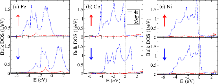
The goal of this section is the analysis of the conductance of ideal, yet plausible one-atom contact geometries for the three ferromagnetic metals (Fe, Co, and Ni) considered in this work. In order to understand the results described below, it is instructive to first discuss the bulk density of states (DOS). The spin- and orbital-resolved bulk DOS of these materials around , as calculated from our tight-binding model, is shown in Fig. 1. The common feature for the three ferromagnets is that the Fermi energy for the minority spins lies inside the bands. This fact immediately suggests Cuevas1998a ; Scheer1998 that the orbitals may play an important role in the transport. Occupation of the and orbitals for both spins is around 0.25 and 0.4 electrons, respectively. For the majority spins the Fermi energy lies close to the edge of the band. The main difference between the materials is that for Fe there is still an important contribution of the orbitals, while for Ni the Fermi level is in a region where the and bands become more important. The calculated values of the magnetic moment per atom (in units of the Bohr magneton) of for Fe, for Co, and for Ni are reasonably close to literature values.CRC1999
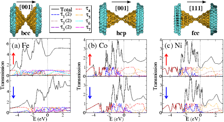
We now proceed to analyze in detail the conductance of some ideal one-atom geometries, which are chosen to simulate what happens in the last conductance plateau before the breaking of the nanowires. First, we consider the one-atom contacts shown in the upper panels of Fig. 2. These geometries are constructed starting with a single atom and choosing the nearest neighbors in the next layers of the ideal lattice along the direction indicated with an arrow. In the case of Fig. 2, for Fe (bcc lattice with a lattice constant of Å) the contact is grown along the [001] direction, for Co (hcp lattice, lattice constant Å) along the [001] direction (parallel to “ axis”) and for Ni (fcc lattice and lattice constant Å) along the [111] direction. The number of atoms in the central region has been chosen large enough, such that the transmission does not depend anymore on the number of layers included. Moreover, as explained in the previous section, the central region is coupled seamlessly to ideal surfaces grown along the same direction.
Let us start describing the results for the Fe one-atom contact of Fig. 2(a). There we present the total transmission for majority spins and minority spins as a function of energy as well as the individual transmissions. We find for this particular geometry the spin-resolved conductances ( for majority spins) and ( for minority spins), which results in a total conductance of . The conductance for the majority spins is the result of up to 8 open channels (with a transmission higher than 0.01), while for the minority spins there are 11 channels giving a significant contribution to . The large number of channels and consequently the high conductance, are partially due to the large apex angle of of the pyramids. As a consequence of this, the layers next to the central atom couple to each other and give rise to a significant tunnel current that proceeds directly without traversing the central atom. On the other hand, the larger number of channels for the minority spins is due to the key contribution of the orbitals that dominate the transport through this spin species, while for the majority spins the and orbitals are the more relevant ones. This fact, which is supported by the analysis of the local density of states (not shown here), is a simple consequence of the position of the Fermi energy and the magnitude of the spin splitting (see discussion of the bulk DOS above).
We define the spin polarization of the current as
| (7) |
With this definition we find a value of for the Fe one-atom contact of Fig. 2(a). In order to compare to the polarization of bulk we have calculated the transmission at the Fermi energy for a series of contact geometries where a bar of constant diameter bridges the two lead surfaces. When the diameter of the bar (or central region of the contact) is increased, the polarization grows continously and saturates at a value of for a contact containing atoms in 7 layers. This is in good agreement with the experimental value obtained using normal-metal-superconductor point contacts.Soulen1998 Notice that can be quite different in an atomic contact as compared to bulk. This is because the conductance is not simply controlled by the DOS at the Fermi energy, but the precise coupling between the orbitals in the constriction plays a crucial role.
For the Co contact depicted in Fig. 2(b) the transmission is lower than for Fe, partly due to the smaller apex angle of the hcp pyramids. In this case we find for majority spins and for minority spins, summing up to a total conductance of . There are 3 channels contributing to and 8 channels to . As in the case of Fe, the larger number of channels for the minority spins is due to the position of the Fermi level and the resulting contribution of the orbitals for this spin. We also find that there is a small but non-negligible contribution of channels that proceed directly without crossing the central atom. This explains, in particular, why one has 8 channels for the minority spins, although at most 6 bands ( and ) have a significant DOS at this energy. Turning to the current polarization, we find a value of for the Co one-atom contact. We also calculate the polarization for a series of Co bars with increasing diameter in hcp direction. As the diameter increases, the polarization decreases to a value of for a contact containing five layers of atoms each, again in good agreement with the experiment.Soulen1998 Notice again that not only the magnitude of for a one-atom contact can be quite different from bulk, but also its sign can be the opposite.
Finally, the Ni contact shown in Fig. 2(c) exhibits conductances of for majority and for minority spins, adding up to a total conductance of . The consists of 3 channels, due to the contribution of the and orbitals, and contains 6 channels, which originate from the contribution of the orbitals. In this case we find a value for the polarization of . Once more we have investigated the polarization of bulk Ni in a series of large Ni bars in fcc direction. Interestingly, the polarization decreases from for a contact of atoms in four layers to for a contact consisting of atoms in four layers.
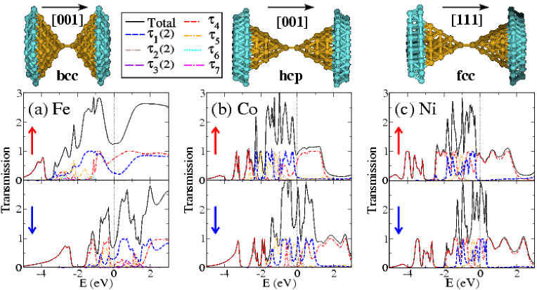
Now we turn to the analysis of the geometries shown in the upper panels of Fig. 3. The difference with respect to the geometries of Fig. 2 is the presence of a dimer in the central part of the contacts. This type of geometry has frequently been observed in molecular dynamics simulations of atomic contacts of Al (Ref. [Jelinek2003, ]) and Au (Ref. [Dreher2005, ]) and we also find them in our simulations of Ni contacts in the last stages of the breaking process.Pauly2006
Inserting a dimer in the geometries of Fig. 2 results in a larger separation of the pyramids to the left and right of the central atom and therefore in a weaker coupling between the layers next to the dimer. This is particularly important in the case of Fe. The resulting transmission for the Fe contact with a central dimer is shown in Fig. 3(a), where one can see that only 3 channels remain for the majority spins, yielding , while for the minority spins 3 channels contribute to . The total conductance is and the polarization . For Co the contact of Fig. 3(b) with a central dimer exhibits and , summing up to a total conductance of . The transmission is formed by 3 channels for the majority spins (with one clearly dominant) and 6 channels for minority spins and polarization is . Finally, for the Ni contact in Fig. 3(c) with a central dimer, a single channel contributes to and 4 channels add up to . This means that one has a total conductance of , while the current polarization adopts a value of .
Beyond the precise numerical values detailed in the previous paragraph, we would like to stress the following conclusions from the analysis of Fig. 3. First, the transport contribution of the minority spins is dominated by the orbitals, which give rise to several channels (from 3 to 5 depending on the material). Second, for the majority spins there is a smaller number of channels ranging from 3 for Fe to 1 for Ni. This contribution is dominated by the and orbitals for Fe and only by the orbitals for Co and Ni. The relative contribution and number of channels of the two spin species is a simple consequence of the position of the Fermi level and the magnitude of the spin splitting. In particular, notice that as we move from Fe to Ni, the Fermi energy lies more and more outside of the band for the majority spins, which implies that the number of channels is reduced for this spin species. In particular, for Ni a single majority spin channel dominates. On the other hand, notice that the conductance values for the different contacts lie typically above , which is precisely what is observed experimentally.Untiedt2004
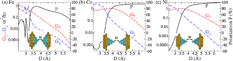
So far, we have analyzed geometries for the so-called contact regime where the nanowires are formed. As shown above, in this case the contribution of the bands makes it difficult to obtain large values of the current polarization. In this sense, one may wonder what happens in the tunnel regime when the contact is broken. In order to address this issue, we have simulated the breaking of the contacts by progressively separating the electrodes of the dimer geometries of Fig. 3. In this way, we have computed the conductance and the current polarization as a function of the tip separation and the results for the three materials are summarized in Fig. 4. With increasing one enters the tunnel regime, which is characterized by an exponential decay of the conductance. In the regime shown in the graphs, Fe does not yet exhibit an exponential decay. In contrast, the conductances for Co and Ni are well fitted by an exponential with Å-1 and Å-1, respectively. These values are in reasonable agreement with the WKB approximationMessiah , which yields Å-1 using a work function of eV.CRC1999 Notice that deep in the tunnel regime for the three materials, the conductance for the majority spins largely overcomes the value of the minority spin conductance. This results in positive values of the current polarization and, in particular, for Co and Ni it reaches values very close to 100%.
The origin of these huge values of current polarization in the tunnel regime is the following. In this regime the current is, roughly speaking, a convolution of the local densities of states on the tips weighted with the squared hoppings of the relevant orbitals of both electrodes. The hoppings between orbitals decay faster with the separation of the tips than the corresponding hoppings of the orbitals. Due to this faster decay, the conduction is then dominated by the orbitals and since the on-site energy for the minority spins lies further away from the Fermi energy than the corresponding one for majority spin, the transmission through the latter one is much higher giving rise to a very large positive spin polarization in the tunneling regime.
IV Role of atomic disorder
In the previous section we have seen that the orbitals play an important role in transport. These orbitals are rather localized on the atoms and the energy bands that they give rise to have relatively flat dispersion relations. Therefore, one would expect the contribution of these orbitals to the transport to be very sensitive to the contact geometry. Indeed, in the previous section we have seen examples in which, by changing the structure of the central part of the contacts, one can even change the sign of the current polarization. Motivated by these results, we study in this section in a more systematic manner how disorder in the atomic positions influences the conductance of one-atom contacts.
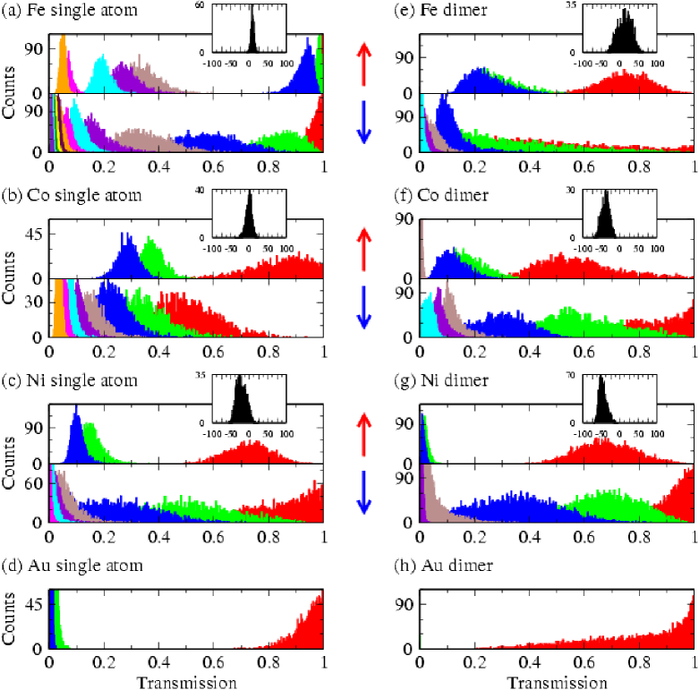
In order to simulate the role of disorder we have studied the conductance of contacts in which the atomic positions in the central cluster have been changed randomly using the geometries of Figs. 2 and 3 as starting points. In Fig. 5 we present an example of such a study, where we show histograms of the channel-resolved transmissions at the Fermi energy for both spins constructed from around 3000 realizations of disorder for each contact. The amplitude of the random displacement in each direction was in this case 0.05 times the lattice constant. Similar results for contacts of the noble metal Au are also shown for comparison. Moreover, for the ferromagnetic materials the insets show corresponding histograms of the spin polarization of the current.
Let us now discuss the main features of the transmission histograms. First, they show that the number of channels obtained for the ideal geometries in the previous section is robust with respect to disorder, although the transmission coefficients depend crucially on the precise atomic positions. Second, for the minority spins one has a non-negligible contribution of at least 5 channels, which originate mainly from the bands. For the majority spins the number of channels is clearly smaller and is progressively reduced as we go from Fe to Ni. This is particularly obvious in the panels of the dimer structures, where one can see that for Fe there are three sizable channels and the contribution of the smallest two decreases for Co and Ni. As explained in the previous section, this is a consequence of the relative position of the Fermi energy in these three metals. For the latter case of Ni, one channel clearly dominates the majority spin conductance, but second and third channels are still present. Thus, unlike in the case of noble metals such as Au, which only have a single channel (see Fig. 5), for ferromagnetic materials conductance quantization is not expected. Third, the peaks in the histograms for the ferromagnetic metals are much broader (especially for the minority spins) than for Au. This is due to the higher sensitivity of the bands to the atomic positions, as compared to the orbitals that dominate the transport in the case of Au. This higher sensitivity is a result of the anisotropic spatial dependence of the orbitals.
In addition, we have calculated the values of the current polarization for each realization of disorder in the contacts. The resulting histograms can be found as insets in the panels of Fig. 5. The peaks in each histogram are centered around the polarization values of the corresponding ideal geometries of Sec. III.
To end this section we would like to make the following comment. In this work we have analyzed the conductance of some ideal one-atom geometries and the influence of disorder. These types of calculations are very valuable to elucidate the nature of the electrical conduction in atomic wires. However, one has to be cautious in establishing a direct comparison between such theoretical results and the experiments because of the lack of knowledge of the exact geometries realized experimentally. Ideally, the theory should aim at describing the conductance histograms, which contain the full experimental information without any selection of the data. This is precisely what we have done for Ni contacts in our recent work [Pauly2006, ] and refer the reader to it for further details.
V Conclusions
In this work we have presented a theoretical analysis of the conductance of one-atom thick contacts of the ferromagnetic 3 metals Fe, Co, and Ni. Our calculations are based on a self-consistent tight-binding model that has previously been successful in describing the electrical conduction in non-magnetic atomic-sized contacts. Our results indicate that the orbitals of these transition metals play a fundamental role in the transport, especially for the minority-spin species. In the case of one-atom contacts, these orbitals combine to provide several partially open conduction channels, which has the following important consequences. First, there is no conductance quantization, neither integer nor half-integer. Second, the current in these junctions is, in general, not fully spin-polarized. Third, the conductance of the last plateau is typically above . Finally, both the conductance and the spin polarization of the current are very sensitive to the contact geometry. The ensemble of these theoretical findings supports the recent observations of Untiedt et al.,Untiedt2004 while it is in clear contradiction with the observations of half-integer conductance quantization.Elhoussine2002 ; Shimizu2002 ; Gillingham2002 ; Rodrigues2003 ; Gillingham2003a ; Gillingham2003b
It is interesting to mention that in the tunnel regime, when the contacts are actually broken, the nature of the conduction changes radically. We have shown that in this case the transport is mainly dominated by the orbitals and the spin polarization of the current can reach values close to +100%.
We want to stress that in all our calculations we have assumed that the atomic contacts were formed by single magnetic domains. In this sense, it would be interesting to see how the conductance in these calculations is modified by the presence of domain walls in the contact region. The first theoretical studies Smogunov2002 ; Velev2004 ; Bagrets2004 ; Jacob2005 along these lines show that the presence of a domain wall cannot conclusively explain the appearance of huge magnetoresistance values reported in the literature. Garcia1999
Recently, the so-called anisotropic magnetoresistance has been observed in ferromagnetic atomic contacts.Viret2002 ; Keane2006 ; Bolotin2006b ; Viret2006 This effect, in other words the dependence of the resistance on the relative alignment of the current and the magnetization, stems from the spin-orbit coupling, and can give rise to a correction to the resistance on the order of 1% in bulk ferromagnets.Mcguire1975 Although the correction can be bigger for atomic-sized contacts,Bolotin2006b ; Viret2006 it is nevertheless expected to be a relatively small effect. The main ingredient that determines the conduction in the ferromagnets is the electronic structure, which is what we have described in this work.
VI Acknowledgments
We thank Elke Scheer, Magdalena Hüfner, Sören Wohlthat, and Michel Viret for helpful discussions. MH, JKV, FP, and JCC were supported financially by the Landesstiftung Baden-Württemberg within the “Kompetenznetz Funktionelle Nanostrukturen”, the Helmholtz Gemeinschaft within the “Nachwuchsgruppen-Programm” (Contract No. VH-NG-029) and the DFG within the CFN. DF was supported by the European Commission through the Research Training Network (RTN) “Spintronics”. MD and PN appreciate the support by the SFB 513.
References
- (1) N. Agraït, A. Levy Yeyati, and J.M. van Ruitenbeek, Phys. Rep. 377, 81 (2003).
- (2) J.C. Cuevas, A. Levy Yeyati, and A. Martín-Rodero, Phys. Rev. Lett. 80, 1066 (1998).
- (3) E. Scheer, N. Agraït, J.C. Cuevas, A. Levy Yeyati, B. Ludoph, A. Martín-Rodero, G. Rubio, J.M. van Ruitenbeek and C. Urbina, Nature 394, 154 (1998).
- (4) J.C. Cuevas, A. Levy Yeyati, A. Martín-Rodero, G. Rubio Bollinger, C. Untiedt, and N. Agraït, Phys. Rev. Lett. 81, 2990 (1998).
- (5) B. Ludoph, N. van der Post, E.N. Bratus’, E.V. Bezuglyi, V.S. Shumeiko, G. Wendin, and J.M. van Ruitenbeek, Phys. Rev. B 61, 8561 (2000).
- (6) C. Sirvent, J.G. Rodrigo, S. Vieira, L. Jurczyszyn, N. Mingo, and F. Flores, Phys. Rev. B 53, 16086 (1996).
- (7) J.L. Costa-Krämer, Phys. Rev. B 55, R4875, (1997).
- (8) K. Hansen, E. Laegsgaard, I. Stensgaard, and F. Besenbacher, Phys. Rev. B 56, 2208 (1997).
- (9) F. Ott, S. Barberan, J.G. Lunney, J.M.D. Coey, P. Berthet, A.M. de Leon-Guevara, and A. Revcolevschi, Phys. Rev. B 58, 4656 (1998).
- (10) H. Oshima and K. Miyano, Appl. Phys. Lett. 73, 2203 (1998).
- (11) T. Ono, Y. Ooka, H. Miyajima, and Y. Otani, Appl. Phys. Lett. 75, 1622 (1999).
- (12) F. Komori and K. Nakatsuji, J. Phys. Soc. Jap. 68, 3786 (1999).
- (13) N. García, M. Muñoz, and Y.-W. Zhao, Phys. Rev. Lett. 82, 2923 (1999).
- (14) B. Ludoph and J.M. van Ruitenbeek, Phys. Rev. B 61, 2273, (2000).
- (15) M. Viret, S. Berger, M. Gabureac, F. Ott, D. Olligs, I. Petej, J.F. Gregg, C. Fermon, G. Francinet, and G. Le Goff, Phys. Rev. B 66, 220401(R) (2002).
- (16) F. Elhoussine, S. Mátéfi-Tempfli, A. Encinas, and L. Piraux, Appl. Phys. Lett. 81, 1681 (2002).
- (17) M. Shimizu, E. Saitoh, H. Miyajima, and Y. Otani, J. Magn. Magn. Mat. 239, 243 (2002).
- (18) D. Gillingham, I. Linington, and J. Bland, J. Phys.: Condens. Matter 14, L567 (2002).
- (19) V. Rodrigues, J. Bettini, P.C. Silva, and D. Ugarte, Phys. Rev. Lett. 91, 96801 (2003).
- (20) D. Gillingham, C. Müller, and J. Bland, J. Phys.: Condens. Matter 15, L291 (2003).
- (21) D. Gillingham, I. Linington, C. Müller, and J. Bland, J. Appl. Phys. 93, 7388 (2003).
- (22) C. Untiedt, D.M.T. Dekker, D. Djukic, and J.M. van Ruitenbeek, Phys. Rev. B 69, 081401(R) (2004).
- (23) M. Gabureac, M. Viret, F. Ott, and C. Fermon, Phys. Rev. B 69, 100401(R) (2004).
- (24) C.-S. Yang, C. Zhang, J. Redepenning, and B. Doudin, Appl. Phys. Lett. 84, 2865 (2004).
- (25) J.L. Costa-Krämer, M. Díaz, P.A. Serena, Appl. Phys. A 81, 1539 (2005).
- (26) K.I. Bolotin, F. Kuemmeth, A.N. Pasupathy, and D.C. Ralph, Nano Lett. 6, 123 (2006).
- (27) Z.K. Keane, L.H. Yu, and D. Natelson, Appl. Phys. Lett. 88, 062514 (2006).
- (28) K.I. Bolotin, F. Kuemmeth, and D.C. Ralph, cond-mat/0602251.
- (29) M. Viret, M. Gabureac, F. Ott, C. Fermon, C. Barreteau, G. Autes, and R. Guirardo-Lopez, Eur. Phys. J. B 51, 1 (2006).
- (30) A. Martín-Rodero, A. Levy Yeyati, and J.C. Cuevas, Physica C 352, 67 (2001).
- (31) A. Smogunov, A. Dal Corso, and E. Tossati, Surf. Sci. 507, 609 (2002); 532, 549 (2003).
- (32) A. Delin and E. Tosatti, Phys. Rev. B 68, 144434 (2003).
- (33) J. Velev and W.H. Butler, Phys. Rev. B 69, 094425 (2004).
- (34) A. Bagrets, N. Papanikolaou, and I. Mertig, Phys. Rev. B 70, 064410 (2004).
- (35) A.R. Rocha and S. Sanvito, Phys. Rev. B 70, 094406 (2004).
- (36) D. Jacob, J. Fernández-Rossier, and J.J. Palacios, Phys. Rev. B 71, 220403(R) (2005).
- (37) M. Wierzbowska, A. Delin, and E. Tosatti, Phys. Rev. B 72, 035439 (2005).
- (38) H. Dalgleish and G. Kirczenow, Phys. Rev. B 72, 155429 (2005).
- (39) D. Jacob and J.J. Palacios, Phys. Rev. B 73, 075429 (2006).
- (40) M.J. Mehl and D.A. Papaconstantopoulos, Phys. Rev. B 54, 4519 (1996).
- (41) M. Häfner, P. Konrad, F. Pauly, J.C. Cuevas, and E. Scheer, Phys. Rev. B 70, 241404(R) (2004).
- (42) M. Brandbyge, N. Kobayashi, and M. Tsukada, Phys. Rev. B 60, 17064 (1999).
- (43) M. Dreher, F. Pauly, J. Heurich, J.C. Cuevas, E. Scheer, and P. Nielaba, Phys. Rev. B 72, 075435 (2005).
- (44) J.K. Viljas, J.C. Cuevas, F. Pauly, and M. Häfner, Phys. Rev. B 72, 245415 (2005).
- (45) N.C. Bacalis, D.A. Papaconstantopoulos, M.J. Mehl, and M. Lach-hab, Physica B 296, 125 (2001).
- (46) F. Guinea, C. Tejedor, F. Flores, and E. Louis, Phys. Rev. B 28, 4397 (1983).
- (47) D.R. Lide, CRC Handbook of Chemistry and Physics, 79th Edition (CRC Press, Boca Raton, Florida, 1998).
- (48) A. Messiah, Quantum Mechanics, Vol. I (Wiley & Sons, 1958).
- (49) P. Jelínek, R. Pérez, J. Ortega, and F. Flores, Phys. Rev. B 68, 085403 (2003).
- (50) F. Pauly, M. Dreher, J.K. Viljas, M. Häfner, J.C. Cuevas, and P. Nielaba, cond-mat/0607129.
- (51) R.J. Soulen, Jr., J.M. Byers, M.S. Osofsky, B. Nadgorny, T. Ambrose, S.F. Cheng, P.R. Broussard, C.T. Tanaka, J. Nowak, J.S. Moodera, A. Barry, and J.M.D. Coey, Science 282, 85 (1998).
- (52) T.R. Mcguire and R.I. Potter, IEEE Trans. Magn. 11, 1018 (1975).