Permanent address: ] Institute of Radio Engineering and Electronics, Russian Academy of Science, Mokhovaya 11, 101999, Moscow, Russia
Subgap conductivity in SIN-junctions of high barrier transparency
Abstract
We investigate the current-voltage characteristics of high-transparency superconductor-insulator-normal metal (SIN) junctions with the specific tunnel resistance . The junctions were fabricated from different superconducting and normal conducting materials, including Nb, Al, AuPd and Cu. The subgap leakage currents were found to be appreciably larger than those given by the standard tunnelling model. We explain our results using the model of two-electron tunnelling in the coherent diffusive transport regime. We demonstrate that even in the high-transparency SIN-junctions, a noticeable reduction of the subgap current can be achieved by splitting a junction into several submicron sub-junctions. These structures can be used as nonlinear low-noise shunts in Rapid-Single-Flux-Quantum (RSFQ) circuitry for controlling Josephson qubits.
I Introduction
In the past decades, the mechanisms of the conductivity through the superconductor-insulator-normal metal (SIN) tunnel interface have been extensively studied. Due to the superconducting energy gap in the quasiparticle density of states, the current through such an interface is generally suppressed at low temperatures, , and subgap bias voltages, , giving rise to a low-voltage nonlinearity in the -curve Tinkham . Recently this, the most common property of SIN-contacts has been found to be rather useful, e.g., for reducing generation of quasiparticles by building the current shunts into the Josephson-junction qubits Banishing or for avoiding an extra decoherence Zorin-SIN in all-Josephson RSFQ-qubit integrated systems Semen .
In particular, the thermal noise produced by the resistively shunted Josephson junctions in a standard RSFQ-circuitry, brings into being an additional source of qubit decoherence Zorin-SIN . It was shown however that this effect can be minimized, by using the nonlinear damping that is provided by an SIN-junction of low asymptotic resistance, , and a high value of the nonlinearity parameter , where is the zero-bias conductivity of the shunt. The dynamics of SIN-shunted Josephson junctions has recently been analyzed in detail on the basis of a standard tunnelling model of the SIN-junction (see Ref. Zorin-microscopic ). The feasibility was demonstrated to ensure both a high damping at the characteristic Josephson frequency , where is the characteristic voltage and the critical current, and, due to the high impedance of the SIN-junction at subgap voltages, a sufficiently low noise at qubit frequencies of typically up to .
The first experiments on SIN-shunted Nb SIS Josephson junctions Zorin-SIN have proven the feasibility of the overdamped regime at . At the same time, however, an unexpectedly weak subgap nonlinearity of the SIN-junctions was observed. In particular, the value of , measured at in an SIN-junction with a specific tunnel resistance of , was much smaller than the values which are typical of opaque barriers (see, e.g., Refs. Opaque ; PothierGueron ), and also far below the simple estimates made for the tunnelling model, yielding a large subgap suppression factor Tinkham . In view of the previous data, it would be an even more challenging task to achieve a high nonlinearity in SIN-junctions of very low specific resistance, e.g., for the SIN-junctions based on superconducting Al Zorin-SIN , as required for RSFQ operation at qubit temperatures .
In this paper, we address subgap conductance phenomena in SIN-junctions of very high transparency. In particular we found that the degree of nonlinearity of the measured -curves is consistent with predictions of the two-electron tunnelling model which has been developed in a ballistic regime by Blonder, Tinkham and Klapwijk (BTK) BTK and modified by Hekking and Nazarov HekNazPRL ; HekNazPRB to account also for interference contributions due to coherent electron diffusion. In earlier experiments, the spatial coherence was clearly demonstrated by Pothier et al. PothierGueron in the form of a periodical dependence of the low-bias conductance of the so-called NS-QUID interferometer on the magnetic flux. A spatially coherent enhancement of the two-electron tunnelling amplitude makes the junction conductance topology-dependent. This effect was observed as zero-bias conductance anomaly in a thin-film planar NS-interface, which was compared in Ref. Xiong with the BTK ballistic transport through an edge-type NS-contact. In our experiment, we compare the values of the nonlinearity parameter for different junction topologies, varying the junction sizes and/or the width of the adjacent diffusive electrode. We show that a sufficiently strong nonlinearity can be obtained in submicron SIN-contacts with even high-transparency barriers, i.e. in the case of interest for RSFQ-qubit applications.
II Design of samples
Two techniques were applied for fabricating the samples. The large reference junctions ”NbAuPd” and ”NbAl” (see Table 1) were made in a standard sandwich technique which is usually applied for RSFQ-devices (see, e.g., Refs. Dolata ; Balashov ), on the basis of a Nb trilayer, patterned with the help of optical lithography. Both samples had a sophisticated multilayered structure which made a particular analysis of the SIN-junction component difficult. For example, the junction ”NbAl” consisted of the metal stack with a pronounced proximity effect between the AuPd and the top Nb layers, and, possibly, between the bottom Nb and the covering Al, separated by a thin oxide barrier only. These Nb-based samples were characterized in a He4-cryostat at temperatures down to . The data for these two samples, shown in Table 1, represent our rough estimations.
For the sake of simplicity and flexibility of the design, all other junctions were fabricated by means of Dolan’s shadow evaporation process Dolan . The complete structures were deposited in-situ from the e-gun through the single e-beam-patterned PMMA/Ge/Copolymer mask with free-hanging bridges. The junctions were formed on the overlapping areas of the first and the subsequent shifted layers, deposited through the same openings in the mask but at different tilting angles of the wafer in respect to the incident material flow. The -curves were measured at in a dilution refrigerator.
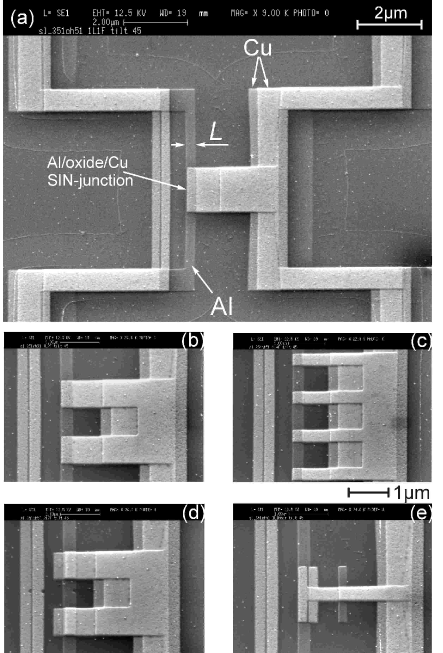
The bottom layer of all shadow-evaporated junctions was made of aluminum, with a thickness of , and oxidized in a very mild regime (see below) to form a thin tunnel barrier. To be able to put several different structures on the same chip, we used besides a two-layer also a three-layer design, with Cu-, Cu/Cu- or Al/Cu-layers building the top electrodes of the junctions. The junctions ”SINTOP” and ”SINBOT” were simple two-layer structures with the tunnel areas differing by the factor of two, both oxidized for 5 min at an oxygen pressure of , which resulted in a specific barrier resistance . A somewhat more complicated layout was used for the junctions ”1L1F” to ”2L4F” which were fabricated on the next wafer. The top junction electrode was made either of a single layer [the top Cu film in the ”1Lxx”- junctions, see, e.g., Fig. 1(a-c),(e)] or of a double-layer composition [a composition of the middle and the top Cu films in the ”2Lxx”-junctions, see, e.g., Fig. 1(d)], evaporated in two consecutive steps, with an additional tilting of the wafer in between. Accordingly, two different thicknesses of the top electrodes, and , were obtained. This wafer was oxidized for 5 min at lower pressure, , in order to obtain an even more transparent barrier. Although all junctions had the same Al bottom layer with the same oxidation step, two different values of were found: for the ”1Lxx”-junctions, and for the ”2Lxx”-junctions. A similar effect was observed for the samples ”SISN” and ”SISNSIN”. In our opinion, this variation is specific to low-dose oxidation processes and arises due to a prolonged oxidation of the Al by adsorbed oxygen in the areas which are not being covered by the middle layer of Cu.
The junctions ”1L2F” to ”2L4F”, ”SISN” and ”SISNSIN” were designed in a ”split-finger” layout [see Figs. 1(b-d)] by subdividing the junction into 2 or 4 narrower sub-junctions with a partial width each, as listed in Table 1. The neighboring fingers of Cu formed, together with the superconducting Al sections, the closed loops of the area . In contrast to the other samples, the normal metal electrodes in the junctions ”1L1Fmin” and ”1L2Fmin” were made in a special ”electron confinement” shape [Fig. 1(e)]: The width of the adjacent wire was reduced further to 1/4 of while the tunnel area was kept identical to that in the samples ”1L1F” and ”1L2F”, respectively.
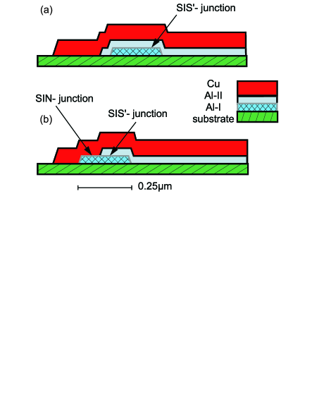
The top electrode of junctions in the samples ”SISN” and ”SISNSIN”, both fabricated on the same wafer, consisted of two different metals, Al and Cu, which formed slightly shifted shadows in such a way that, in the sample ”SISN”, the junction was designed to be effectively of type ”superconductor-insulator-superconductor” with a proximity-reduced gap (SIS’). In the sample ”SISNSIN”, the junction of the same total area was made up of such an SIS’ to the half with an Al/oxide/Cu SIN-contact (see the cross-sections in Fig. 2).
| Sample code | Materials | Tunnel junction area, () () | Thicknesses, , (nm) | (K) | ||||
|---|---|---|---|---|---|---|---|---|
| NbAuPd | Nb/AlO/AuPd | 24 | 180,100 | 1.4 | 16 | 380 | 95 | 6 |
| SINTOP | Al/AlO/Cu | 0.52 | 30,50 | 0.03 | 27 | 27 | 140 | 5.1 |
| SINBOT | Al/AlO/Cu | 0.51 | 30,50 | 0.03 | 54 | 27 | 360 | 6.6 |
| 1L1F | Al/AlO/Cu | 0.242 | 30,30 | 0.05 | 29 | 15 | 90 | 3.1 |
| 1L1Fmin111In these samples, the normal electrode is of ”electron-confinement” shape (see the text). | Al/AlO/Cu | 0.242 | 30, 30 | 0.05 | 32 | 15 | 64 | 2 |
| 1L2F | Al/AlO/Cu | 2(0.241) | 30,30 | 0.05 | 28 | 15 | 88 | 3.1 |
| 1L2Fmin111In these samples, the normal electrode is of ”electron-confinement” shape (see the text). | Al/AlO/Cu | 2(0.241) | 30,30 | 0.05 | 42 | 15 | 113 | 2.6 |
| 1L4F | Al/AlO/Cu | 4(0.240.5) | 30,30 | 0.05 | 31 | 15 | 177 | 5.7 |
| 2L2F | Al/AlO/Cu | 2(0.241) | 30,60 | 0.05 | 11 | 5 | 22 | 2 |
| 2L4F | Al/AlO/Cu | 4(0.240.5) | 30,60 | 0.05 | 11 | 5 | 37 | 3.4 |
| SISN | Al/AlO/Al/Cu | 2(0.250.5) | 30,30,60 | 0.026 | 44 | 11 | 1.9k | 43 |
| SISNSIN | Al/AlO/Al/Cu+Al/AlO/Cu | 2(0.12/0.12222For SISN- and SIN-partial junctions, respectively.0.5) | 30,30,60 | 0.026 | 63 | 11/22222For SISN- and SIN-partial junctions, respectively. | 3.3k | 52 |
| NbAl | Nb/AlO/Al/AlO/AuPd/Nb | 100 | 90,100,100,500 | 1.45 | 1.4 | 150 | 1.4k |
III Results and discussion
Typical -characteristics of high-transparency SIN-junctions are shown in Fig. 3. As expected, significant subgap leakage currents were observed in most of the SIN-junctions, even at the temperature , resulting in a strong smearing of the superconducting gap corner and in rather moderate values of 1–10 (see Table 1). The appreciable excess subgap current at low temperatures is commonly attributed to the resonant two-electron transport channel due to Andreev reflection Andreev . To interpret our data, we first make estimations within the simplified ballistic BTK model, which put aside the electron scattering effects in the electrodes. Using Eq.(17) of BTK , it is straightforward to derive simple expressions for the subgap conductance at :
| (1) |
and the BTK nonlinearity parameter:
| (2) |
whereby the dimensionless barrier strength BTK characterizes the transparency of the NS interface, , and are the Fermi energy and wavenumber, respectively and enters the phenomenological repulsive barrier potential . For a thin tunnel barrier of the simplest, rectangular shape with a height and a thickness , which is the Fermi wavelength, can be expressed as
| (3) |
by matching the well-known plane-wave transmission coefficient (see, e.g., LandauLifshits ) with that of BTK, , which is provided in Ref. BTK for electrons in the normal state.
The straightforward evaluation using Eqs. (2) and (3) and the parameters of the idealized Al/AlOx-barrier, (see, e.g., Refs. McBride ; Maezawa ) and (see the discussion below), as well as and , which are typical for Al, results in the values and and predicts the suppression of the subgap conductivity much stronger than found in our experiment.
Important corrections can be made to the calculations if we take a note of the fact that the barriers under consideration are as thin as a single monolayer of Al oxide. The value of accepted above presents an average barrier thickness of the plane junction with the specific capacitance (derived from the Coulomb offset voltage of the similarly oxidized single-electron transistors LotkhovJAP2004 , cf. also Zant ), and the dielectric constant Maezawa . For such thin oxide layers, it is plausible to expect considerable local deviations of the relative barrier thickness, even for the cleanest tunnel interface.
Possible models for the fine structure of very thin barriers have recently been discussed for junctions of type Nb/AlOx/Nb with current densities in a wide range, Maezawa ; Zant ; Kleinsasser . In Refs. Zant ; Kleinsasser , the barrier is supposed to consist of different areas with a certain number of oxide monolayers, including a statistically large amount of local pinholes of lateral size , with no single monolayer of oxide at all, dominating in the current of the whole junction. In contrast to this, the model of a uniform, continuously growing barrier was suggested by Maezawa et al. Maezawa as a more realistic, predicating upon that oxide is formed on top of a granular Al film with a locally different surface orientation of the crystal planes. Our argument is that small, but finite values, , corresponding to our experimental value (see Fig. 6 of Ref. BTK ), rather relate to the picture of a thin, but finite tunnel barrier, at least on the mesoscopic scale . Moreover, on the microscopic scale , the ballistic transport model accounting for the pinhole effects is not adequate; the relevant approach here relates to the electron diffraction, which makes the tunnelling picture non-local Diffraction .
To build a quantitative model, we assume a uniform distribution of the barrier thickness around the mean value , i.e. , with a constant probability density , and consider an independent electron transport through the areas within the junction with different local barrier strengths. The effective zero-bias nonlinearity can then be found as the ratio of the average asymptotic and the zero-bias conductivities :
| (4) |
best matching the experimental range of 2–7 in Al-based SIN junctions for 0.8–0.9, i.e., for the realistic barriers with a thickness of up to two oxide monolayers.
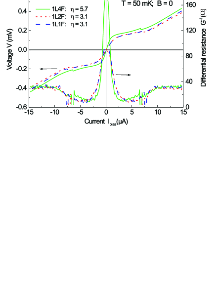
So far we have been able to obtain a reasonable, though rough, estimation of the zero-bias nonlinearity of SIN junctions within the scope of the ballistic BTK model. A more detailed insight can be gained, by comparing the subgap transport properties in SIN junctions of the same transparency but of different size. For example, in Fig. 3 the voltage-current characteristics of the single-junction structure ”1L1F” [Fig. 1(a)] is compared to those of the split-finger interferometer structures ”1L2F” and ”1L4F” [Fig. 1(b,c)]. All three structures have the same total tunnel area and, therefore, similar asymptotic resistances, but they differ with regard to the number and the width of the partial junctions. In none of the split-finger interferometer structures, a periodic dependency of the -curves on the magnetic field was observed, which indicates the absence of inter-junction coherence effects such as those reported earlier for different structure dimensions by Pothier et al. PothierGueron . This property of our structures is obviously due to the normal-metal sections of each loop being, in total, longer than the interference length in a diffusive conductor HekNazPRL and, when used in practice, it makes damping on the base of the split-finger SIN-junction flux insensitive. Independent tunnelling in the sub-junctions enables a parallelization of the SIN-contacts, when a low shunting resistance is required.
For the larger junctions ”1L1F” and ”1L2F”, with , the value of does not vary with the junction width. On the contrary, for the parallel connection of the four smaller, -wide sub-junctions in sample ”1L4F”, the value of is nearly twice as large. The same tendency is to be seen for the samples ”2L2F” and ”2L4F” with slightly different parameters (see Table 1). The observed dimensional effect can be interpreted following the model of Hekking and Nazarov HekNazPRL ; HekNazPRB which accounts for spatially coherent contributions to the Andreev conductance due to two-electron diffusion. According to this model, the coherence factors, and thus the subgap conductance, are expected to increase with the junction size until saturation occurred at . For small junctions of size , this effect can be evaluated using the relation Eq. (12) of Ref. HekNazPRB which was derived for a normal wire in a tunnel contact to a superconducting sheet, rewritten in the form:
| (5) |
where is the specific conductivity of the normal electrode. In our experiment, the validity of Eq. (5) was confirmed by a simple comparison of the nonlinearity parameter values in the junctions ”1L2F” (), and ”2L2F” with [the layout shown in Fig. 1(d)] with a single and a double layer of Cu in the top electrodes, correspondingly. The times larger value of for ”1L2F” arises as the ratio 3 of the specific barrier resistances, multiplied by the ratio 1/2 of the thicknesses of the top electrodes.
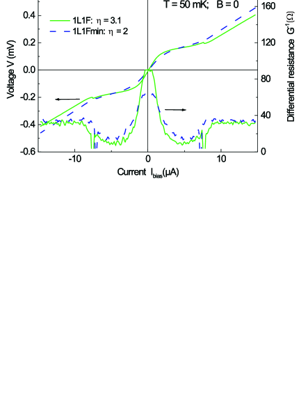
Our data also clearly demonstrate the effect of the ”confinement” shape for the normal wire. As seen in Fig. 4, the zero bias differential resistance of such a sample ”1L1Fmin” [shown in Fig. 1(e)] is times lower than that of the ”plain” junction ”1L1F”, even despite its higher value of . This tendency also shows in the samples ”1L2F” and ”1L2Fmin”. From this, we can conclude that those configurations of the top electrode where the diffusion volume for the back-scattered electrons is restricted to the closer vicinity at the tunnel barrier result in a larger Andreev conductance, which is consistent with the predictions of the model Ref. HekNazPRL ; HekNazPRB .
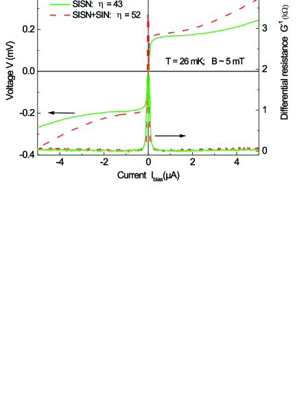
A considerably higher nonlinearity of the -curves, shown in Fig. 5, was observed in the junctions ”SISN” and ”SISNSIN”, where the top electrode was made of a smaller-gap superconductor, , consisting of superconducting Al, covered by a thicker layer of the normal conductor (Cu), see Fig. 2. Due to the second small gap in the density of states, the two-electron conductance is suppressed at small voltages (see, e.g., Schrieffer ), while the multiple Andreev reflections are expected to decrease at small bias as the processes of the higher order in tunnel transparency Kleinsasser . In experiment, a strong current reduction was found at voltages below (cf. also Taylor ), resulting in larger values of and 52 in the samples ”SISN” and ”SISNSIN”, respectively. A higher ratio in the latter sample can be explained by the lower barrier transparency in the SIN partial junction, see Eq. 5. A small critical supercurrent , otherwise observed, could be easily suppressed below the level of fluctuations by a applying perpendicular magnetic field of .
A much larger value was measured in the sample ”NbAl”, at the temperature which slightly exceeds the superconducting transition point for Al. The layer of Al was originally considered in this structure to form a normal-metal electrode whereas the ”S” electrode was a proximity superconductor built of an AuPd/Nb bilayer. However, much higher subgap nonlinearity than in the other SIN-junctions indicates, in our opinion, that the Al electrode has a spectrum of states which differs from that of a normal metal. For example, a small gap could be induced in Al by the bottom film of Nb through a very transparent separating tunnel barrier, making the junction effectively an SIS’ type. We believe that the effect of nonlinear damping in SIS structures deserves a separate investigation.
IV Conclusions
We investigated the nonlinearity of the -characteristics of SIN-junctions of high transparency, fabricated with different topologies and composed of various materials. Our data are consistent with the predictions of the two-electron tunnelling model, accounting for the interference contributions in the diffusive scattering regime. A clear enhancement of the nonlinearity was observed in the submicron junctions with planar dimensions smaller than the length of interference . We show that in a split-finger junction layout, tunnelling in partial junctions is independent and flux-insensitive. This property allows a parallelization of these nonlinear and, therefore, low-noise submicron SIN-junctions. A significant increase in the subgap resistance - compared to the SIN-junctions of the similar transparency - was observed in proximity-type SIS’-junctions. This could be the subject of a special study.
The values obtained for the zero-bias and the asymptotic junction resistances allow the SIN-junctions to be implemented in RSFQ-Qubit circuits as low-noise shunts. For example, our junctions with, typically, could provide a sufficient damping for submicron Josephson junctions with . On the other hand, sufficiently long decoherence times, e.g., , as estimated in Ref. Chiao for a tunable flux qubit, coupled to the RSFQ control circuit, can be achieved due to the high zero-bias resistances, , of most of the measured SIN-junctions.
ACKNOWLEDGMENTS
Helpful discussions with Yu. V. Nazarov, J. Niemeyer, J. P. Pekola, H. Pothier and D. Vion are gratefully acknowledged. The work was partially supported by the EU through the projects RSFQubit and EuroSQIP, and by Deutsche Forschungsgemeinschaft with the project NI 253/7-1.
References
- (1) M. Tinkham, Introduction to Superconductivity (Second Edition, Dover Publications Inc., Mineola, 2004) pp. 75-76.
- (2) K. M. Lang, S. Nam, J. Aumentado, C. Urbina, and J. M. Martinis, IEEE Trans. Appl. Supercond. 13, 989 (2003)
- (3) A. B. Zorin, M. I. Khabipov, D. V. Balashov, R. Dolata, F.-I. Buchholz, and J. Niemeyer, Appl. Phys. Lett. 86, 032501 (2005).
- (4) V. K. Semenov and D. V. Averin, IEEE Trans. Appl. Supercond. 13, 960 (2003); D. S. Crankshaw, J. L. Habif, X. Zhou, T. P. Orlando, M. J. Feldman and M. F. Bocko, ibid., p. 966; M. Wulf, X. Zhou, J. L. Habif, P. Rott, M. F. Bocko and M. J. Feldman, ibid., p. 974; A. M. Savin, J. P. Pekola, D. V. Averin and V. K. Semenov, cond-mat/0509318 (submitted to J. Appl. Phys.).
- (5) A. B. Zorin, E. M. Tolkacheva, M. I. Khabipov, F.-I. Buchholz, and J. Niemeyer, cond-mat/0512615.
- (6) A. Kastalsky, L. H. Green, J. B. Barner, and R.Bhat, Phys. Rev. Lett. 64, 958 (1990); J. P. Castle et al., Czechoslovak J. Phys., 46, Suppl. S5, 2897 (1996); S. Gueron, H. Pothier, N. O. Birge, D. Esteve, and M. H. Devoret, Phys. Rev. Lett. 77, 3025 (1996).
- (7) G. E. Blonder, M. Tinkham, and T. M. Klapwijk, Phys. Rev. B. 25, 4515 (1982).
- (8) F. W. J. Hekking and Yu. V. Nazarov, Phys. Rev. Lett. 71, 1625 (1993).
- (9) F. W. J. Hekking and Yu. V. Nazarov, Phys. Rev. B. 49, 6847 (1994).
- (10) H. Pothier, S. Gueron, D. Esteve, and M. H. Devoret, Phys. Rev. Lett. 73, 2488 (1994); Physica B 203, 226 (1994).
- (11) P. Xiong, G. Xiao, and R. B. Laibowitz, Phys. Rev. Lett. 71, 1907 (1993).
- (12) R. Dolata, M. I. Khabipov, F.-I. Buchholz, W. Kessel, and J. Niemeyer, Inst. Phys. Conf. Ser. 2, 1709 (1995).
- (13) D. V. Balashov, M. I. Khabipov, A. B. Zorin, S. A. Bogoslovsky, F.-I. Buchholz, and J. Niemeyer, 10th International Superconductive Electronics Conference, September 5-9, 2005, Noordwijkerhout, The Netherlands. Extended Abstracts, edited by H. Rogalla and A. Brinkman (University of Twente, The Netherlands, 2005), P-C.06.
- (14) G. J. Dolan, Appl. Phys. Lett. 31, 337 (1977); J. Niemeyer, PTB-Mitt. 84, 251 (1974).
- (15) A. F. Andreev, Zh. Eksp. Teor. Fiz. 46, 1823 (1964) [Sov. Phys. JETP 19, 1228 (1964)].
- (16) L. D. Landau, E. M. Lifshits, Quantum Mechanics (non-relativistic theory) (Pergamon Press, New York, 1965).
- (17) O. Iwanyshyn and H. J. T. Smith, Phys. Rev. B 6, 120 (1972); T. A. Fulton and L. N. Dunkleberger, J. Appl. Phys. 45, 2283 (1974).
- (18) D. McBride, G. Rochlin, and P. Hansma, J. Appl. Phys. 45, 2305 (1974).
- (19) M. Maezawa, M. Aoyagi, H. Nakagawa, I. Kurosawa, and S. Takada, Appl. Phys. Lett. 66, 2134 (1995).
- (20) S. V. Lotkhov, S. A. Bogoslovsky, A. B. Zorin, and J. Niemeyer, J. Appl. Phys. 95, 6325 (2004).
- (21) H. S. J. van der Zant, R. A. M. Receveur, T. P. Orlando, and A. W. Kleinsasser, Appl. Phys. Lett. 65, 2102 (1994).
- (22) A. W. Kleinsasser, R. E. Miller, W. H. Mallison, and G. B. Arnold, Phys. Rev. Lett. 72, 1738 (1994).
- (23) A. B. Zorin and K. K. Likharev, Fiz. Nizk. Temp. 4, 713 (1978) [Sov. J. Low Temp. Phys.4, 340 (1978)]; A. B. Zorin and K. K. Likharev, J. Phys. (France) 39, No. 8 Suppl., C6-573-574 (1978).
- (24) J. R. Schrieffer and J. W. Wilkins, Phys. Rev. Lett. 10, 17 (1963).
- (25) B. N. Taylor and E. Burstein, Phys. Rev. Lett. 10, 14 (1963).
- (26) F. Chiarello, cond-mat/0602464.