Single Electron Transport in electrically tunable nanomagnets
Abstract
We study a single electron transistor (SET) based upon a II-VI semiconductor quantum dot doped with a single Mn ion. We present evidence that this system behaves like a quantum nanomagnet whose total spin and magnetic anisotropy depend dramatically both on the number of carriers and their orbital nature. Thereby, the magnetic properties of the nanomagnet can be controlled electrically. Conversely, the electrical properties of this SET depend on the quantum state of the Mn spin, giving rise to spin-dependent charging energies and hysteresis in the Coulomb blockade oscillations of the linear conductance.
pacs:
73.23.Hk,85.75.-d,78.67Hc,78.55.EtNanomagnets attract interest both because of their intriguing behavior as relatively macroscopic quantum objects Tejada and their potential technological applications as magnetic bits Cobalt and qbits Loss-Nature . The two fundamental properties of a nanomagnet are the net spin of its ground state, and its magnetic energy anisotropy tensor, that governs the stability of the magnetization with respect to quantum and thermal fluctuations. Although recent experiments show that single molecule magnets like Mn12 CM1 ; CM2 or metallic Co Ralph-SET nanoparticles can be probed in single-molecule transistor measurements, their properties can hardly be tuned once they are fabricated. Here we show that a single electron transistor (SET) consisting of a II-VI quantum dot doped with a single Mn atom behaves like a tunable nanomagnet whose magnetization and anisotropy axis can be reversibly manipulated electrically. Conversely, the conductance and charging energy of the tunable nanomagnet depend on the quantum state of the Mn spin and are not uniquely determined by the gate and the bias voltage.
Our proposal is based on two independent progress in nanofabrication. On one side, the fabrication and optical probing of single CdTe quantum dots doped with a single Mn atom Besombes1 ; Besombes2 ; Besombes3 . In the absence of carriers, the spin of the Mn is free. Optical excitation of electron-hole pairs into the dot shows that the Mn spin is exchange coupled to both the electron and the holeBesombes1 ; Besombes2 ; Besombes3 ; JFR05 . On the other side, the control of the charge state of II-VI semiconductor quantum dots with single electron accuracy has been experimentally demonstrated Klein-Nature ; Forchel-APL as well as in the case of single-Mn doped quantum dots Leger-2006 and Mn-doped GaAs islands Wunderlich .
Hamiltonian. We consider a CdTe quantum dot (QD) doped with a single Mn, weakly coupled to two metallic and non-magnetic electrodes. The dot can be gated so that either the valence band or the conduction band is in resonance with the metallic reservoir and the number of either electrons or holes is varied at will. The total Hamiltonian reads: Here is the Hamiltonian for the diluted magnetic semiconductor (DMS) quantum dot. In analogy with the the standard model Furdyna for bulk DMS, describes confined conduction band electrons and valence holes interacting with a localized Mn spin , denoted as , via a local exchange interaction. QD carriers occupy localized spin orbitals with energy which are described in the envelope function approach JFR04 ; JFR05 ; dot-holes . In the case of valence band holes the 6 band Kohn-Luttinger Hamiltonian, including spin orbit interaction, is used as a starting point to build the quantum dot states dot-holes . The second quantization Hamiltonian of the isolated dot describes the states of reads:
| (1) |
Here creates a band carrier in the single particle state of the quantum dot, which can be either a valence band or a conduction band state. The first term in the Hamiltonian describes non interacting carriers in the dot and the second term describes the exchange coupling of the carriers and the Mn. We neglect interband exchange so that () if both and belong to the conduction band states (valence band states). In contrast, we include exchange processes by which a carrier is scattered between two different levels of the dot that belong to the same band. The matrix elements of both valence and conduction band spin density, evaluated at the location of the Mn atom, are given by . They depend strongly on the orbital nature of the single particle level in question. In the case of conduction band we neglect spin orbit interactions so that is rotationally invariant JFR04 . In contrast, strong spin orbit interaction of the valence band makes the Mn-hole interaction strongly anisotropic JFR05 ; Leger-2006 ; dot-holes and it varies between different dot levels. Following previous work JFR05 ; JFR04 ; dot-holes confinement is described by a hard wall cubic potential with . Although real dots are not cubic, this simple model dot-holes ; JFR05 provides an excellent description of the Hamiltonian of the Mn spin coupled to the carriers, which is able to account for the non-trivial single-exciton PL spectra both for neutral Besombes1 ; Besombes2 ; Besombes3 and chargedLeger-2006 single-Mn doped CdTe QD.
Coulomb repulsion between carriers is described within the constant interaction model Beenakker-REV : , where is the total capacitance to the external circuit, and are the capacitances of the left and right junctions ( is the bias voltage) and is the capacitance to the gate (with voltage ). is the extra charge in the dot. We do not consider dots with orbital degeneracy for which Coulomb correlations, neglected in this paper, are relevant Govorov05a ; PRL2005-Haw . Finally, and describe the metallic electrodes and and are the standard spin-conserving tunneling Hamiltonian that couple the metallic reservoirs and the dot.
We first discuss the properties of the eigenstates of for isolated dots () with a given number of carriers, interacting with the Mn atom. We show results for two dots of CdTe with , and different (dot A) and (dot B), both doped with 1 Mn atom. The neutral dot has 6 degenerate states, corresponding to the equivalent spin orientations of the Mn spin. This degeneracy is lifted in the presence of either electrons or holes. We focus on dots with a odd number of carriers (open shells) for which the interactions are stronger JFR04 ; Govorov05a and study how the magnetic anisotropy varies with the number of carriers. The spectra of dots with 1 electron, 1 hole and 3 holes are shown in figs. 1a, 1b and 1c respectively for dot A (and also QD for the case of 1 hole). The effect of intra-level exchange is magnified in the inset of fig. 1a. In figure 1b and 1c we only show the low energy manifold for dot A with 1 and 3 holes. The 12 states of the low energy manifold for and are formed mainly by the two lowest energy electronic configurations of the dot with a single unpaired fermion coupled to the 6 Mn states. The low energy sector of can be described by an intra-level effective HamiltonianLeger-2006 : where are the Pauli matrices operating on the isospin space defined by the lowest energy single particle doublet.
Both the absolute and the relative values of , and depend mostly on the spin properties of the external shell of the quantum dot: either conduction band level (), heavy hole () or light hole (). Thereby, the can be controlled reversibly by means of the gate voltage in the same device. The effective Hamiltonian of the Mn coupled to the ”master fermion” in dot A goes from ferromagnetic Heisenberg () when () to antiferromagnetic Ising when () to XXZ (). In dot similar results are obtained, with , which provides a spin-flip term in the case, absent in dot A.

Correspondingly, the spin properties of the ground state also change as a function . In the case of the Mn spin and the conduction band electron couple ferromagnetically to yield a septuplet with . In the case of the ground state doublet corresponds to the Mn spin maximally polarized against the heavy hole spin, and , both for dots A and B. In dot A the rest of the low-energy sector is formed by 5 doublets eigenstates of both and , whereas in dot the small spin-flip interaction mixes and . In the case with , the ground state is not degenerate and the Mn spin is polarized in the plane, minimizing . These differences reflect the spin properties of conduction band electron, heavy hole and light hole respectively.
We now address how these remarkably different magnetic properties occurring in the same dot are reflected in the electrical behavior of the SET. In analogy with previous work Efros ; Waintal-PRL2003 ; Waintal-PRL2005 ; Timm ; Braun1 , we derive a quantum master equation for the dissipative dynamics of the reduced density matrix written in the basis of many-body states . Importantly, this quantum master equation includes the combined dynamics of both populations and coherences. The latter are important because of the intrinsic many-body degeneracies of the QD spectra shown in fig. 1. Assuming that the quantum dot is weakly coupled to the electronic reservoirs (sequential tunneling), the dissipative dynamics of the density matrix is governed by a Markovian kernel, , where can be casted as a vector containing both populations and coherence terms. The matrix contains information about dissipative dynamics of which is governed by the rates:
| (2) |
Here , , is the Fermi function of reservoir r and =1-.The notation implies that states with charge are connected with states with charge . . The coupling to the leads is parametrized by , where is the DOS of the metallic reservoir. Once we obtain the steady state density matrix (namely, ), we can compute the average charge, magnetization and current. To lowest order in , the most general expression for the current can be written as with:
| (3) |
Notice that Eq. (3) includes both diagonal and non-diagonal terms in the density matrix. The latter are important when two degenerate states with are coupled to the same state of via a single tunneling event.
The steady state of a standard SET is uniquely characterized by external voltages Beenakker-REV . For instance, a new charge is accommodated in the dot at precise values of the gate voltage, when the electrochemical potential of the dot (the energy required for adding the th electron to the dot) falls within the bias window . When this condition is met, the number of electrons can vary between and resulting in a single-electron tunneling current. Importantly, in our case the charge and the conductance of the SET depend also on the quantum state of the Mn spin.
In figure 2 we show linear conductance , average charge and diagonal terms of the steady state , as the gate produces the transition between charge zero and chage for both electrons (left panels) and holes (right panels). The initial for the charging simulations is chosen so that only the states are occupied. This initial condition is described by a thermal with 6 equally populated Mn spin states, . We ramp the gate and solve the master equation to obtain the steady state , which is used as initial condition for the next run with higher . In the case of electrons we obtain standard results: a single peak in the curve occurs as the gate is ramped to change the charge of the dot by one unit. In fig. 2c we show the evolution of the steady state populations: The 6 spin states are relaxed altogether in favor of the 7 states of the and states.
The results for holes in QD are remarkably different: in the process of injection of 1 hole the curve shows 3 peaks instead of 1. This results from the lack of Mn spin relaxation ( is a conserved quantity for the entire Hamiltonian including tunneling), which makes the steady different from to the thermal . As the gate brings down into resonance the 2 ground states ( and () with the 6 ground states with , population tranfer only affects states with in both charge sectors (first peak in fig. 2d at meV). Further increase of the gate brings the energy of the the ground state doublet below the states with , which are not depleted because is conserved (fig. 2f). The population transfer only occurs when the second and third doublet of the spectrum, with and are brought down in resonance with the states. This accounts for the other two peaks in the curve as the charge of the dot approaches . Hence, the charging energy for holes depends on the absolute value of the spin of the Mn. The discharge simulation is done analogously. If the initial is such that there is one hole in the QD, the Ising interaction removes the degeneracy among states with different . Only the doubly degenerate ground state of the sector is occupied in thermal equilibrium. As the gate is ramped to discharge the dot, a single peak in the conductance is obtained, corresponding to the resonance condition with between the and states with .
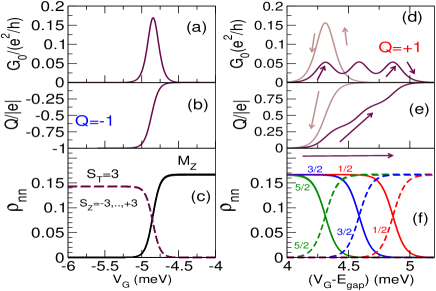
The difference between electrons and holes arises from the different value of a crucial time scale in the magnetic sigle electron transistor: the Mn spin relaxation time, . In the case of QD , is infinite for holes (Ising coupling) which makes the steady state different from the thermal state. In the case of electrons (left panels) the transverse spin interactions make comparable to the charge relaxation time () so that steady and thermal are identical. In real dots doped with one hole, may be long but not infinite. Two independent mechanisms, missing in the simulations shown in the right panels of fig. 2., yield a finite . First, the Mn due to super-exchange with other spins which scales exponentially with the Mn density T1Mn . For bulk Cd0.995Mn0.005Te we have , which is a lower limit estimate for of the QD with a single Mn. The second mechanism is the smallLeger-2006 transverse spin interaction, which is proportional to the light-hole heavy-hole mixing. We have simulated QD , for which spin-flip interaction between the hole and the Mn is small but non-zero resulting in a finite . If we integrate the master equation for the curve displays 2 peaks and hysteretic behaviour. In contrast, if we integrate the master equation for , the system reaches the equilibrium state for each value of so that the curve has a single peak. Therefore, we claim that effects related to incomplete spin relaxation of the dot will be observed subject to two conditions: the finite bandwith of the measurements should be larger than (see for instance ref. (CM2, )) and the pace at which is ramped should be faster than .

The finite bias conductance of the device also depends strongly on the charge state of the dot. In figure 3 we show and curves for dot corresponding to bias-assisted single electron fluctuations between and (fig 3a), and (fig. 3b), and and (fig 3c). Fig. 3d is the analogous of 3b for dot B. Current flows whenever the addition of a fermion is permitted by energy conservation and spin selection rules. The former provides a link between the curve and the energy spectra of dots shown in fig. 1 (since the spectra of dots with and are flat). Interestingly, the for electron tunneling (3-a) shows a zero-magnetic field splitting related to recent experimental observations Gould06 . In turn, has 6(7) peaks in fig. 3b (3d), are similar to the experimental single exciton PL spectra Besombes1 ; Besombes2 ; Besombes3 ; JFR05 .
In summary, we have shown some of the equilibrium and non-equilibrium properties of a semiconductor quantum dot doped with a single Mn atom and wired as a single electron transistor. The different orbital nature of the conduction band electrons, heavy holes and light holes determines both the total spin and the magnetic anisotropy of the dot. In the case of holes, for which Mn spin flip processes are heavily inhibited, we predict different results for the curves depending on whether the system is relaxed to equilibrium or not. In the case of the latter, we predict hysteretic Coulomb blockade oscillations related to the the quantum state of the Mn spin. Because most of the transport properties discussed above are inherent to nanomagnets with long spin relaxation time, our findings might be very general and have implications in recent experiments CM1 ; CM2 ; Wunderlich .
Fruitful discussions with L. Brey, J. J. Palacios, Y. Léger, L. Besombes, J. Cibert, H. Mariette, C. Gould and P. Hawrylak are acknowledged. This work has been financially supported by MEC-Spain (Grants FIS200402356, MAT2005-07369-C03-03, and the Ramon y Cajal Program) and by CAV (GV05-152).
References
- (1) J. Tejada, E. M. Chudnovsky, Macroscopic Quantum Tunneling of the Magnetic Moment, Cambridge University Press, Cambridge (1998)
- (2) M. Jamet, W. Wernsdorfer, C. Thirion, D. Mailly, V. Dupuis, P. M linon, and A. Pérez, Phys. Rev. Lett. 86, 4676 (2001).
- (3) M. Leuenberger, D. Loss, Nature 410, 789 (2001)
- (4) H. B. Heersche et al., Phys. Rev. Let96, 206801 (2006)
- (5) Moon-Ho Jo et al. Nano Lett. 6, 2014(2006);
- (6) M. Deshmuch and D. Ralph, Phys. Rev. Lett. 89, 266083 (2002)
- (7) L. Besombes, Y. L ger, L. Maingault, D. Ferrand, H. Mariette and J. Cibert Phys. Rev. Lett. 93, 207403 (2004)
- (8) L. Besombes, Y. Leger, L. Maingault, D. Ferrand, H. Mariette, and J. Cibert Phys. Rev. B. 71, 161307 (2005)
- (9) Y. Léger L. Besombes, L. Maingault, D. Ferrand, and H. Mariette, Phys. Rev. Lett. 95,047403 (2005)
- (10) J. Fernández-Rossier, Phys. Rev. B.73, 045301 (2006)
- (11) D. L. Klein, R. Roth, A. K.L. Lim, A. P. Alivisatos, and P. L. McEuen Nature 389, 699 (1997)
- (12) J. Seufert, M. Rambach, G. Bacher, A. Forchel, T. Passow, D. Hommel, Appl. Phys. Lett. 82, 3946 (2003)
- (13) Y. Léger L. Besombes, J. Fernández-Rossier, L. Maingault, H. Mariette , Phys. Rev. Lett.97, 107401 (2006)
- (14) J. Wunderlich, Phys. Rev. Lett. 97, 077201 (2006)
- (15) J. K. Furdyna, J. Appl. Phys 64 R29 (1988).
- (16) J. Fernández-Rossier and L. Brey, Phys. Rev. Lett. 93 117201 (2004)
- (17) F. V. Kyrychenko and J. Kossut, Phys. Rev. B70 , 205317 (2004)
- (18) H. van Houten, C. Beenakker, A. A. M. Staring, Single Charge Tunneling, edited by H. Grabert and M. H. Devoret, NATO ASI Series B294, Plenum, New York, 1992.
- (19) A. O. Govorov, Phys. Rev. B72 , 075359 (2005). A. O. Govorov, Phys. Rev. B72 , 075358 (2005).
- (20) F. Qu, P. Hawrylak, Phys. Rev. Lett. 95, 217206 (2005)
- (21) A. Efros, E. Rashba, M. Rosen, Phys. Rev. Lett. 87, 206601 (2001)
- (22) X. Waintal, P. Brouwer, Phys. Rev. Lett.91, 247201 (2003)
- (23) X. Waintal, O. Parcollet, Phys. Rev. Lett.94, 247206 (2005)
- (24) C. Timm, F. Elste Phys. Rev. B73, 235304 (2006)
- (25) M. Braun, J. König, J. Martinek, Phys. Rev. B 70, 195345 (2004)
- (26) J. Lambe and C. Kikuchi, Physical Review 119, 1256 (1960); D. Scalbert et al., Solid State Commun., 66, 571 (1988).
- (27) C. Gould et al., Phys. Rev. Lett. 97, 017202, (2006)