Pinhole and tunneling conduction channels superimposed in magnetic tunnel junction: results and inferences
Abstract
The influence of ballistic channels superimposed on tunneling conduction channels in magnetic tunnel junctions has been studied in a manganese oxide based tunneling device. Inversion of magnetoresistance has been observed in magnetic tunnel junctions with pinhole nanocontacts over a broad temperature range. The tunnel magnetoresistance undergoes a change of sign at higher bias and temperature. This phenomenon is attributed to the parallel conduction channels consisting of spin conserved ballistic transport through the pinhole contact where the transmission probability is close to unity and spin polarized tunneling across the insulating spacer with weak transmittivity. The results seem to resolve a controversy regarding ballistic magnetoresistance in ferromagnetic nanocontacts and establishes that ballistic magnetoresistance do exist even if the previous results are attributed to magnetostriction and magnetostatic force related artifacts.
pacs:
72.25.-b, 73.40.Gk, 75.47.JnI Introduction
The last decade has seen sustained efforts on part of the research community towards achieving large room temperature magnetoresistance at low magnetic field via manipulation of electron spin, driven partly due to the potential applications in memory devices and magnetic field sensors and partly since the subject is interesting from the fundamental point of view. Extensive studies are going on along two major directions: Spin polarized tunneling in ferromagnetic tunnel junction and Spin conserved ballistic transport across ferromagnetic nanocontacts. The situation can become really interesting, as will be shown in this article, when the above two directions interfere with each other.
The story of spin polarized tunneling goes back to the early seventies when Meservey and Tedrow tedrow ; tedrow1 proved that the spin of the electron tunneling from a ferromagnet into a superconductor is conserved and that the conductance is proportional to the density of states of the two electrodes. These observations has led to what is now known as the Julliere model julliere which provides a simple picture for transport in Magnetic Tunnel Junction (MTJ). However, it was the discovery of room temperature Tunnel Magnetoresistance (TMR) jag in which generated immense interest in this field. Recently, the theoretical prediction and subsequent observation of large room temperature magnetoresistance in epitaxial Fe/MgO/Fe structure mgo have triggered a race for achieving even higher value of Tunnel Magnetoresistance.
Different transport regimes can be identified according to the relative size of various length scales corresponding to different scattering mechanisms. An important length scale is the elastic mean free path , which estimates the average distance traversed between successive elastic collisions with static scattering centers. The situation , being the typical length scale of the sample (usually a few nanometer), corresponds to the so called ballistic regime where the electron suffers little or no collision with static impurities and is only limited by scattering with the boundaries of the nanosized conductor. Study of magnetotransport properties in ferromagnetic nanocontacts showing conductance values of a few conductance quanta , started in with the discovery of about magnetoresistance at room temperature in ballistic Ni nanocontacts bmr1 . This experiment was followed by several reports which claimed even higher values of ballistic magnetoresistance bmr2 ; bmr3 ; bmr4 .
Coming back to the experiment in ref. bmr1 , initially a qualitative argument was presented in explaining the results. It was proposed that the density of states and consequently the spin polarization at the nanocontact is significantly larger than bulk Ni. For sufficiently thin domain wall width the electrons can travel across the contact in parallel configuration, while in the antiparallel configuration, faces a strong back-scattering. The same authors in a separate article in the same year bmr , proposed that the essential ingredient for BMR is the condition of nonadiabaticity in ballistic transport across the nanocontact. If the domain wall width at the nanocontact is sufficiently thin so that the spin does not have time to flip then the situation becomes analogous to the spin conserved tunneling in MTJs and the magnetoresistance is related to the transport spin polarization of the electrodes in the same way as the Tunneling Magnetoresistance (TMR) in Julliere julliere or Slonczewski’s model slonc which predicts positive TMR for symmetric electrode MTJ. It was also reported that the ballistic magnetoresistance exhibits an universal scaling property scaling . However, recently, this so called Ballistic Magnetoresistance (BMR) effect in ferromagnetic nanocontacts has attracted attention not for the gigantic positive or negative change in resistance on application of magnetic field but the controversy created by the report of small or no BMR in mechanical ferromagnetic break junctions artifact and the possibility of measurement artifact arising out of the mechanical distortion of the contact geometry on application of magnetic field due to magnetostriction or magnetostatic forces artifact ; artifact1 . It is argued that the very large changes in resistance are due to the effect of magnetostriction or magnetostatic forces that cause the contact to break and reform as the magnetic field is varied and that BMR does not exist. Interestingly, there is another report of extremely large magnetoresistance in oxide based ferromagnetic nanocontacts, which claims that the dominant transport mechanism is not ballistic; it can either be hopping or tunneling coey . We will show that BMR does exist in ferromagnetic nanocontacts although not in that huge magnitude as has been reported earlier.
Observation of inverse tunneling magnetoresistance (TMR; where , are the junction resistances in antiparallel and parallel magnetic configuration of the MTJs respectively.) where the conductance in the antiparallel magnetic configuration is higher than that in the parallel configuration, has been instrumental in understanding some of the important aspects of spin polarized transport in MTJs. For example, the inverse TMR observed in experiments by De Teresa et. al. desci and Sharma et. al. sharma have proved that the transport properties of MTJ depend not only on the ferromagnetic metal electrodes but also on the insulator. The effect of density of states was not apparent until de Teresa et. al. in showed that the TMR depends on the specific bonding mechanism at the electrode-insulator interface and that the choice of the insulator dictates which band is to be selected for tunneling. They prepared two sets of “hybrid” MTJ’s — Co/Al2O3/La0.7SrMnO3 and Co/SrTiO3/La0.7SrMnO3 trilayers. While the former showed positive TMR in the entire bias range, the latter exhibited a spectacular, so called “Inverse TMR” in a wide voltage range. The Inverse TMR was attributed to the negative spin polarization of the d band of Co which is selected for tunneling by the insulator SrTiO3, while the normal positive TMR in the former system is due to the selection of positively polarized s band by Al2O3. A few months before, in , M. Sharma et. al. had already published another significant result on the effect of density of states where composite tunnel barriers were used. An inversion of spin polarization was observed in MTJ’s with Ta2O5/Al2O3 barriers. The tunneling magnetoresistance changes sign with applied voltage. This inversion was attributed to the spin polarizations of the electrode/Ta2O5 interface and the Al2O3/electrode interface being opposite. Generally inverse TMR can occur if the sign of spin polarization of the two electrode-insulator interfaces is opposite in the relevant bias range. This means that while for one electrode, the majority spin tunneling density of states (DOS) is greater than the minority spin DOS, the conduction electrons from the other electrode should be of minority spin character. There is another report on inversion of TMR in asymmetric electrode Ni/NiO/Co nanowire MTJ. Tsymbal et. al. tsymbal1 have shown that there is a finite probability that resonant tunneling via localized impurity state, which is positioned asymmetrically inside the barrier can invert the effective spin polarization of one of the electrodes thus leading to inverse TMR. However, for this to happen, the junction area has to be extremely small, otherwise for larger junction area one has to sum over all the local disorder configurations while calculating the conductance and hence the disorder driven statistical variations in TMR will be less probable.
Unfortunately, the influence of ballistic spin dependent transport (due to the presence of pinhole nanocontacts which connect the two ferromagnetic electrodes) on the magnetoresistive properties of MTJs has not been explored substantially. This problem cannot be ignored since nowadays the emphasis is on fabricating low resistance MTJs using ultra thin insulating spacer, which increases the chances of occurrence of pinhole shorts. Recent simulations have shown that as much as of the current can flow through the pinholes simulation in MTJs even though the bias dependence of differential conductance has positive curvature. It was claimed ballistic1 that ballistic channels in MTJs are not magnetoresistive and the opening up of a spin-independent conduction channel can only reduce the TMR. We will show that the ballistic channel in MTJs are not only magnetoresistive, it, in fact, can cause inverse tunneling magnetoresistance. However, the contribution due to tunneling conduction channel might not be ignored. These two can act as parallel conducting channels. The relative contributions from the two conduction channels – elastic tunneling through the insulating spacer and ballistic spin polarized transport through the narrow pinhole shorts – can change as the temperature and applied bias are varied and magnetoresistive response can change accordingly.
II Experiment, Results and Discussion
The trilayer La0.67Sr0.33MnO3 (LSMO) / Ba2LaNbO6 (BLNO) / LSMO was deposited on single crystalline SrTiO3 (100) substrate held at a temperature C and oxygen pressure mTorr, using pulsed laser deposition. BLNO has a complex cubic perovskites structure and can be grown epitaxially on single crystal perovskite substrates blno1 ; blno2 . The estimated thickness of the insulating spacer from the deposition rate calibration of BLNO is . The microfabrication was done using photo-lithography and ion-beam milling. For further details see ref. soumik ; soumik1 .
Discovery of Giaever tunnelinggiaever for superconductor-insulator-superconductor structures in 1960’s and subsequent studies gave rise to a set of criteria, known as Rowell’s criteria rowell , for determining the quality of the tunnel junction. However, for magnetic tunnel junctions, only three of these criteria are applicable. Exponential thickness dependence of junction resistance. Parabolic differential conductance curves that should be well fitted by rectangular barrier Simmons simmons model or trapezoidal barrier Brinkman model brinkman . Insulating like temperature dependence of junction resistance. It has been observed that MTJs with pinhole shorts can reproduce the first two criteria short1 . Therefore the third criteria stands out as the reliable proof of the quality of the MTJ. The contrasting behavior in the temperature dependence of junction resistance for three MTJs with same junction area and spacer thickness is shown in Fig: 1. While one of the MTJs denoted as MTJ0 show a gross insulator like temperature dependence of junction resistance, the other two MTJs exhibit distinct metallic junction resistance.
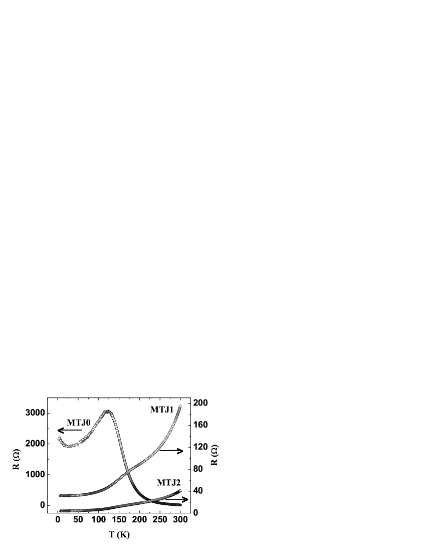

The junction resistance in the absence of magnetic field for MTJ0 shows a distinct peak at around K with a rise at low temperature (Fig: 1), typical of manganite tunnel junctions res ; res1 . Although the low temperature rise in resistance with decrease in temperature is consistent with Rowell’s criteria for tunneling, there is an additional suppression of tunneling density of states at low temperature which makes the temperature dependence of junction resistance much sharper. Above K, the sharp decrease in junction resistance with increasing temperature is attributed to the higher order tunneling via thermally populated impurity states within the barrier. There is still no clear explanation as to what causes the decrease in resistance with decreasing temperature below K. With increase in bias level the temperature dependence of junction resistance becomes weaker. The conductance curves show parabolic voltage dependence. We have fitted the differential conductance vs. voltage curves using asymmetric barrier Brinkman model brinkman in different voltage ranges. The average barrier height and the barrier width turns out to be in the range eV and respectively. The asymmetry in the barrier obtained from the Brinkman model is very small, about mV only and hence the current-voltage characteristics can be well fitted with symmetric barrier Simmons model simmons , producing similar results. The barrier parameters like average barrier height and barrier width are almost temperature independent within the relevant temperature range. All these observations indicate that the device is free of any pinhole shorts and tunneling is the dominant transport mechanism short . The highest value of TMR (as defined earlier) obtained at any bias current and temperature is around . Low TMR value signifies a considerable reduction of spin polarization at the electrode-barrier interface. The tunnel magnetoresistance almost vanishes above K, as is the case generally for manganite tunnel junctions temp .
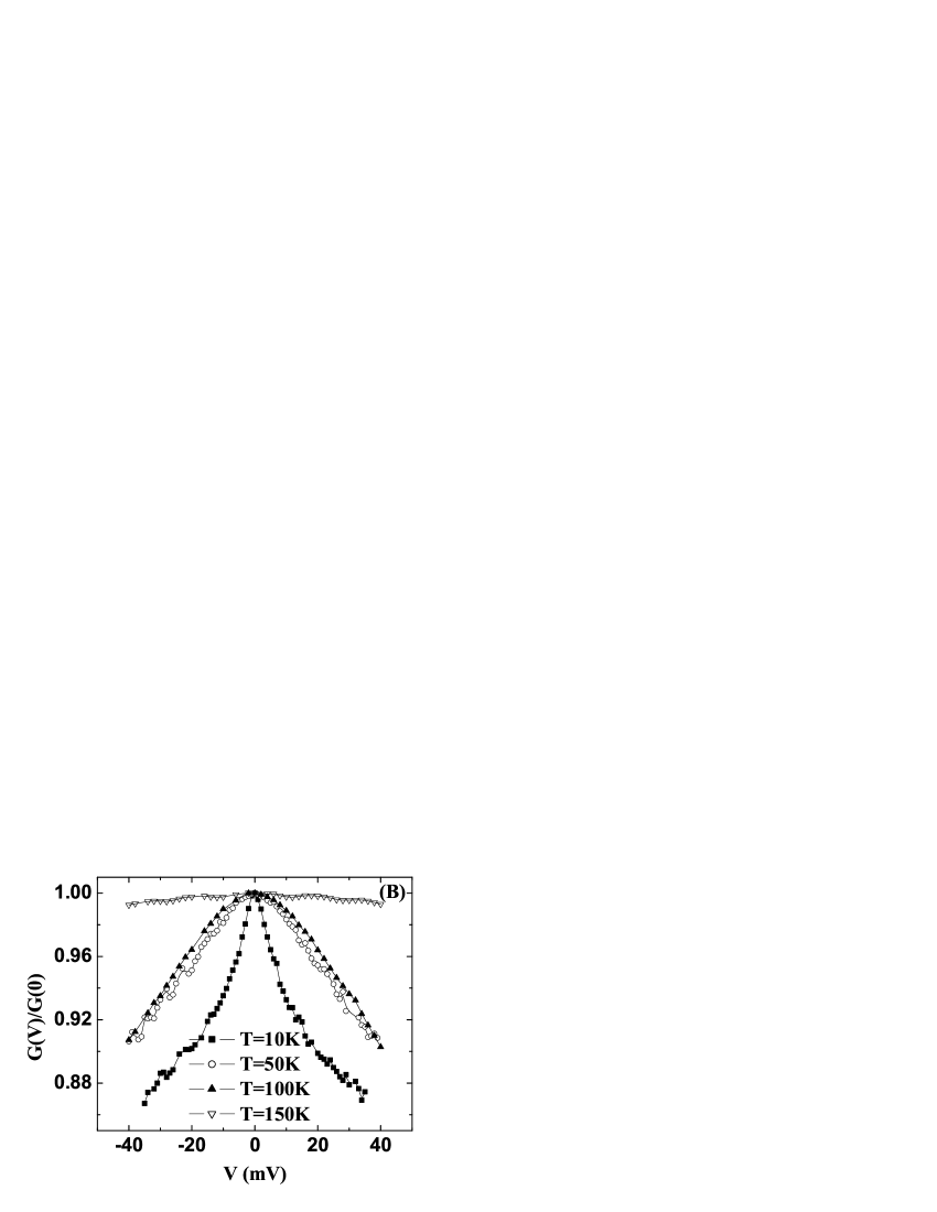
Let us discuss the transport properties of two other MTJs (MTJ1 and MTJ2) fabricated under identical conditions, showing metal-like temperature dependence of junction resistance (Fig: 1). Although these MTJs show non-ohmic voltage dependence, the metallic junction resistance is a strong evidence for the MTJs having pinhole shorts. Each of the MTJs has the same junction area. There is orders of magnitude difference between the junction resistance of the MTJ without pinhole short and those having pinhole shorts. Let us designate the pinhole shorted MTJ with higher resistance as MTJ1 and that having lower resistance as MTJ2. The percentage rise in resistance with increasing temperature for MTJ1 is much larger compared to that of MTJ2. The broad anomaly in the temperature dependence of junction resistance for MTJ1 and MTJ2 in the intermediate temperature region can be considered as being a result of the competition between two parallel conduction channels — tunneling across the insulating spacer with weak transmittivity but large effective interface area and transport through pinhole with high transmittivity and small cross-sectional area. For MTJ1, the anomaly shifts towards higher temperature (around K) as compared to MTJ2 (around K). In this article, we will show that the two MTJs with pinhole shorts exhibit almost identical magnetoresistive properties although the voltage dependence of differential conductance curves have opposite curvatures. While the sample denoted MTJ1 shows positive curvature in the conductance curve at low temperature, the conductance of MTJ2 has negative curvature (Fig: 2A,B) even at K. The MTJs contain metallic nanocontacts through which electrons travel ballistically at low temperature and bias. However, at higher bias, “hot electron” transport through the pinholes results in heat dissipation within the nanocontact region just outside the ballistic channel heat and thus increasing the resistance. At higher bias the back-scattering into the narrow channel increases due to larger phonon density of states at the nanocontact, which reduces the transmittivity resulting in negative curvature in the voltage dependence of differential conductance. However the conduction channel due to tunneling will become less resistive at higher bias since then the electrons will tunnel across relatively thin trapezoidal part of the barrier. As a result, the pinhole short will produce negative curvature in the differential conductance curve while tunneling should cause positive curvature. Although transport in both the MTJs is dominated by conduction through pinhole shorts which is evident in Fig: 1, the strong positive curvature in the voltage dependence of conductance due to tunneling can overcome the weak negative curvature due to transport through the pinholes, resulting in overall positive curvature as observed in MTJ1 (Fig: 2A). At higher temperatures K, MTJ1 shows negative differential conductance around zero bias (Fig: 2A). This anomaly can be understood considering that the tunneling conductance is minimum around this region which is evident from the temperature dependence of junction resistance for the MTJ without pinhole short. In this temperature region the negative curvature due to transport through pinhole short dominates at lower bias and at higher bias positive curvature due to tunneling takes over. At K, the voltage at which the differential conductance takes positive curvature is higher compared to that at and K. This is consistent with the fact that, at K, the tunneling conductance is lower compared to that at and K, which is evident from Fig: 1. The tunneling conductance is much higher at K but still exhibits negative conductance curvature around zero bias, albeit small, for MTJ1 due to the fact that at higher temperature, the positive curvature due to tunneling is significantly weak compared to that at low temperature. Fitting the differential conductance curves with positive curvature for MTJ1 by Brinkman model, the extracted barrier height turns out to be about eV (much higher than the value eV corresponding to MTJs without pinhole shorts) and the barrier width much smaller compared to that of for good MTJs. The extracted value for barrier height increases while the barrier width decreases as the temperature is increased. Although the value of the barrier parameters, in the present case, carry no physical significance, temperature dependence of the barrier parameters is a reconfirmation of the MTJ having pinhole shorts short .
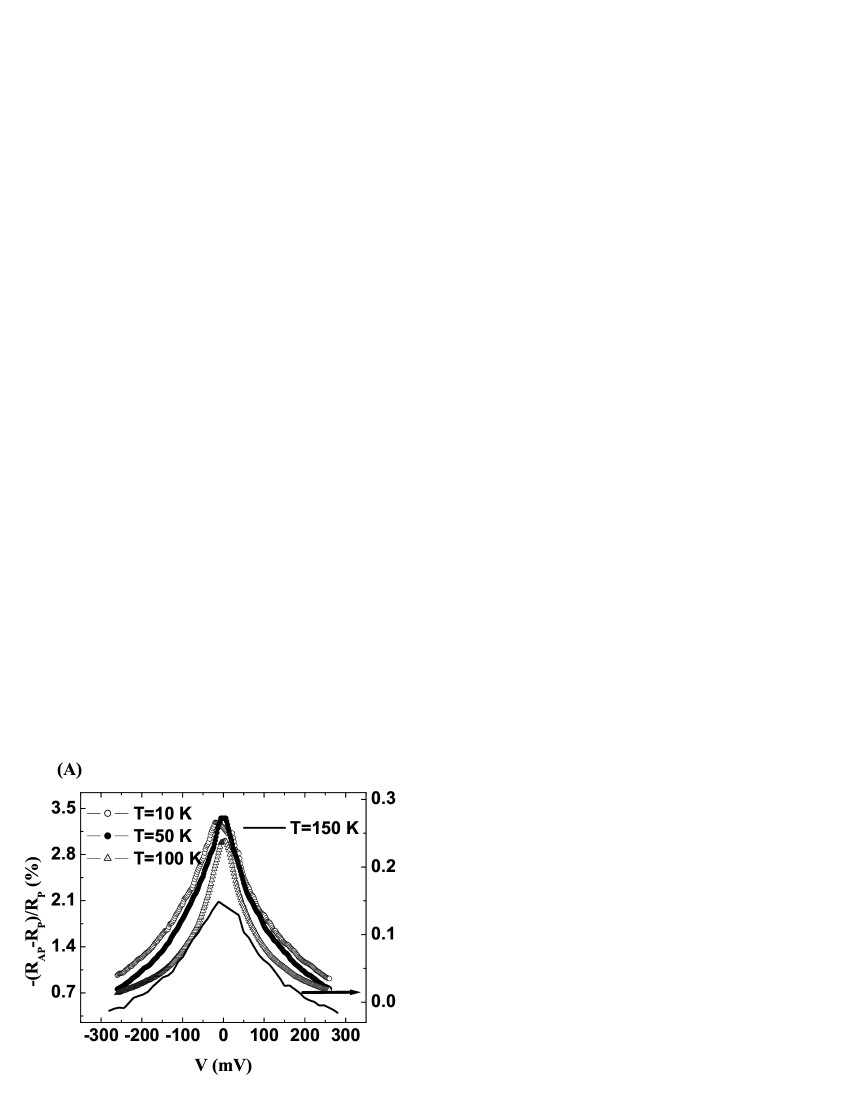
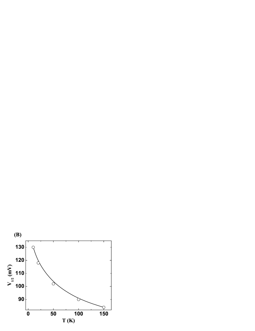
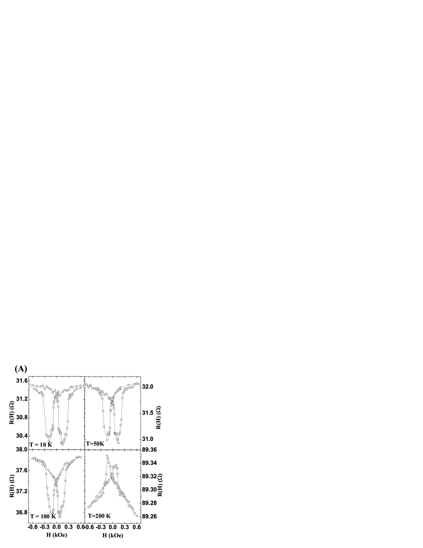
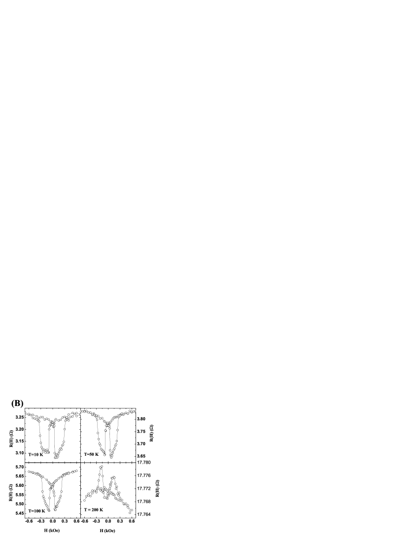
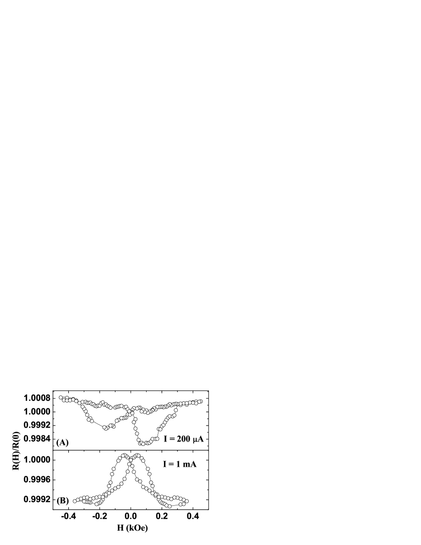
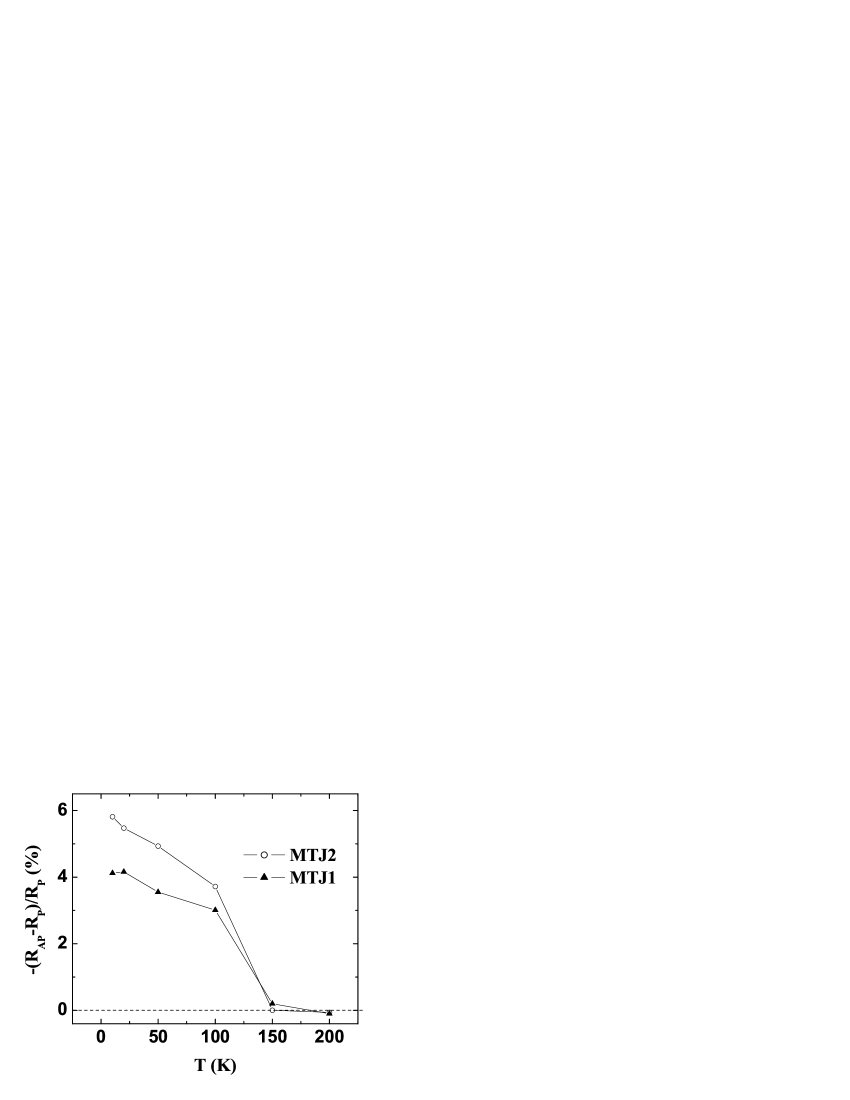
Inverse TMR is observed for both MTJs over a broad temperature range K (Fig: 3). The value of inverse TMR decreases with increasing temperature. For MTJ1 the value of inverse TMR is at K which reduces to about at K while for MTJ2 it is about at K, which almost vanishes at K. Above K, the situation is the opposite – ordinary positive TMR is observed. At K, the positive TMR exhibited by MTJ1 is about while that for MTJ2 is (Fig: 3A,B). The bias dependence of TMR for MTJ1 has some interesting features. At K, it is observed that above mV, the TMR changes sign (Fig: 4A). A clear evidence of such inversion is highlighted in Fig: 5A,B where MTJ1 shows inverse TMR at bias current while at , exhibits positive TMR. However, at lower temperatures, there is no evidence of such inversion with increasing bias (Fig: 4A). The bias voltage at which the inverse TMR reaches half its maximum value which is denoted by , becomes smaller as temperature is increased as shown in Fig: 4B. It is to be noted that MTJ2 with lower junction resistance shows higher inverse TMR values and lower positive TMR value. The temperature dependence of TMR is described in Fig: 6, which shows an abrupt decrease in the value of inverse TMR above K.
The observed phenomenon can be explained as follows. The present system can be considered as being equivalent to two ferromagnetic metal electrodes connected by ballistic nanoscale metallic channels along with a conduction channel connected in parallel which describes tunneling across the insulating spacer. For the case of two identical ferromagnets connected by a nanocontact, the ballistic magnetoresistance (BMR) bmr is given by,
where is the spin polarization, is the domain wall width and is the Fermi wave vector, being the measure of the spin non-conservation in the current through the nanocontact. Because of the function , the magnetoresistance decays rapidly for , which indicates that the electron spin can follow the magnetization change inside the domain wall adiabatically. Therefore, the essential ingredient for BMR is the condition of nonadiabaticity in ballistic transport across the nanocontact. In the limit of vanishing domain wall width , spin flipping by domain wall scattering is absent. Then is unity and the electron spin is conserved during transmission (the factor decreases with the increase of the product ). Hence we arrive at the well known Julliere formula for tunneling magnetoresistance. Thus there seems to be no difference in the spin conserved ballistic transport through nano-sized pinholes or elastic spin polarized tunneling. However there is a stark contrast in the transmittivities for the two conduction channels. In case of normal elastic tunneling through insulating barrier the tunneling probability is finite but small and decays exponentially with increasing barrier width. On the other hand, the transmittivity through the metallic pinhole nanocontact is close to unity.
At low temperature, the electron transfer from one ferromagnetic lead to another occurs dominantly through the metallic pinhole shorts. Hence, according to ref. bmr , the ballistic magnetoresistance should follow the Julliere or Slonczewski’s model for spin polarized tunneling and should give positive TMR for MTJs with identical electrodes. However, in our case, inverse TMR is observed. The reason probably lies in the fact that the model does not take into account the effect of high transmittivity and the possibility of different transmission coefficients of the electrons in the majority and minority spin bands. The model reduces to Julliere model in the non-adiabatic limit. However, there is an agreement that the generalized Julliere model is valid in the limit of very weak transmission probability zhang . Tae-Suk Kim kim has very recently put forward a theoretical model for spin polarized transport through a narrow channel. Using the transfer Hamiltonian approach and the non-equilibrium Green’s function method, Kim has shown that when the spin is conserved in transport through a nanoscale channel and the transmittivity is close to unity, there is a possibility of inverse TMR. According to Kim’s model, transmission probabilities in the parallel () and anti-parallel () magnetic configuration of the two electrodes (assuming that the spin polarizations of the two electrodes are the same) are given as,
where and are the transfer rates for majority and minority spins respectively. When the transmission probability is small, i.e. , , which means that the transmission probability in the parallel configuration is greater than that in the anti-parallel configuration i.e. the TMR is positive. The conditions for zero TMR or are given as, which is a trivial solution and implies that spin polarizations at the Fermi level for both the electrodes is zero and is applicable for nonmagnetic tunnel junctions. The non-trivial solution for zero TMR with spin polarization , resides at the boundary between two regions corresponding to and and is given by,
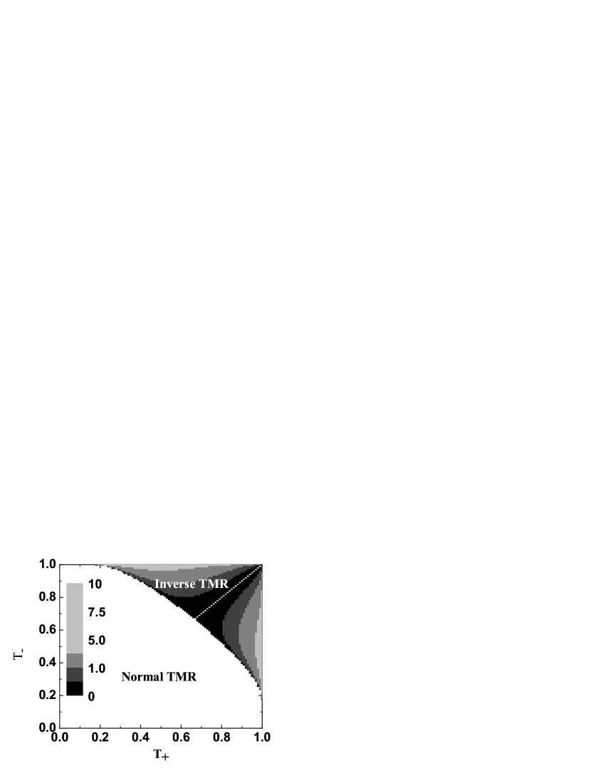
To be more precise, the combinations satisfying the above equation constitutes a curve in space with separating the regions corresponding to normal and inverse TMR. The region close to the origin belongs to normal positive TMR. The region away from the origin contains higher values for and which correspond to inverse TMR.
The transmission probabilities for the majority () and and minority () spin band are related to as follows,
Replacing by in the expression for and , the TMR values [] can be calculated numerically for all possible values of . The transmission probabilities, and , can be expressed in terms of as
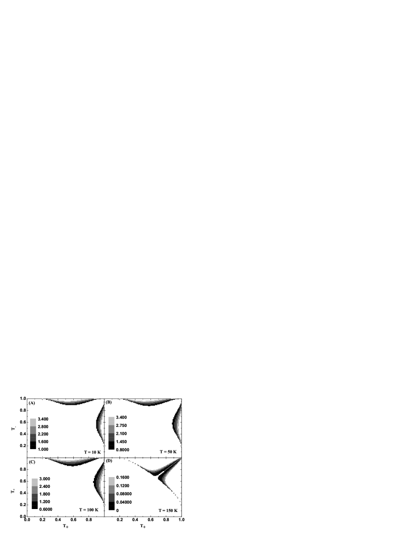
The theoretically allowed values of (, ) for inverse TMR and how the allowed values of (, ) evolve with the change in temperature for MTJ1, within the bias range mV, are shown in Fig: 7 and Fig: 8, respectively, along with the corresponding inverse TMR values. Interestingly, there is an upper bound to the theoretically allowed values of inverse TMR, about which is a little above the highest experimentally obtained value of inverse TMR for our system of about . Therefore, one can conclude that the sign of magnetoresistance will decide whether the transport is truly in the ballistic regime (transmittivity close to unity).
Thus, when transmission probability is closer to unity i.e. and there is an imbalance in the transmission probabilities for the majority spin and the minority spin, inverse TMR occurs. The contribution due to the parallel tunneling conduction channel has been neglected for simplicity of calculation. This will, of course, lead to underestimation of the allowed values of particularly in the high temperature region where the relative contribution of the tunneling conduction channel will be substantial. The calculation suggests that, larger the imbalance between and , the greater is the value of inverse TMR as can be seen from Fig: 7. Up to K, the allowed values of stay away from the line (Fig: 8A,B,C). However, as the temperature is increased further, the imbalance in the transfer rates of majority and minority spins diminishes drastically and the allowed values congregate near (Fig: 8D). The increase in bias also reduces the imbalance between the transmittivities in the two bands as can be seen from the shaded map for each temperature. The fact that for MTJ2 the contribution due to pinhole conduction is higher compared to MTJ1 is consistent with MTJ2 exhibiting higher value of inverse TMR.
Here one is forced to ask questions about the origin of minority spin states since La0.67Sr0.33MnO3 is supposed to be a “transport half-metal”. Although La0.67Sr0.33MnO3 is generally considered to be having almost full spin polarization, Andreev reflection experiments have confirmed the existence of minority spin states which will be particularly influential in the ballistic limit of transport minority . When the point contact Andreev reflection is ballistic the calculated value of spin polarization of La0.67Sr0.33MnO3 is less compared to the case when the contact is diffusive. Since the minority spin states are more localized compared to majority spin states, the minority spins do not contribute to transport spin polarization when the contact is diffusive and hence gives higher value of spin polarization. In this regard, it would be worth mentioning that the authors, in a previous article, had proposed the existence of minority spin tunneling states in La0.67Sr0.33MnO3 soumik . If the values of and are interchanged the TMR remains the same. However, the physically acceptable situation is where is greater than , since the minority spin states are generally regarded as being more localized compared to the majority spin states.

The change from inverse TMR to a positive one at higher bias at K can be attributed to the fact that at higher bias electrons tunnel through relatively thin trapezoidal part of the barrier such that the contribution due to elastic tunneling increases which gives rise to positive TMR. On the other hand, there are several reasons for the decrease of inverse TMR at higher bias due to transport through the narrow channel. Local generation of heat within the nanocontact region at higher bias leads to increased thermal spin fluctuation and resistance at the nanocontact which reduces the inverse TMR. The back-scattering into the narrow channel increases as a result of larger phonon density of states at the nanocontact, reducing the transmittivity and hence the inverse TMR. In our case, the normal positive TMR is observed at K, where elastic tunneling across the insulating spacer with weak tunneling probability is dominant and the electron-phonon interaction pushes the transport through the pinhole into diffusive regime. Oxide-based tunnel junctions with pinhole shorts are better suited to exhibiting inverse TMR than MTJs with transition metal electrodes since in that case there is high probability of the pinhole shorts getting oxidized which would lead to weak transmittivity through the narrow channel. Another important factor is that the mobility in the majority and the minority spin channel in such systems is vastly different and this imbalance is crucial for exhibition of inverse TMR.
Lastly, the point which demands serious attention is on the controversy regarding the existence of ballistic magnetoresistance. Even if the claims that the previous reports of ballistic magnetoresistance suffers from magnetostrictive or magnetostatic force related artifacts are true there is certainly no reason to conclude that Ballistic Magnetoresistance does not exist. Kim’s model and our observation should settle the issue that Ballistic Magnetoresistance can be observed subjected to the following conditions: The contact should be truly ballistic. There should be clear imbalance in the the transmittivities for the majority and minority spin bands. In the true ballistic limit of transport across ferromagnetic nanocontacts, the resistance in parallel magnetic configuration should be higher than the antiparallel configuration.
III Summary
This article deals with two important aspects of spin dependent transport in artificial ferromagnetic nanostructures — firstly, how the existence of ballistic conduction channels can drastically influence the magnetoresistive properties of magnetic tunnel junctions, and secondly, which has more general implications, what should be the sign of magnetoresistance in ferromagnetic nanocontacts in the truly ballistic limit. We have presented a direct experimental evidence that pinhole shorts through the insulating spacer in a magnetic tunnel junction can cause inverse tunnel magnetoresistance when the transmission probability is close to unity, which is an indicator that Julliere and Slonczewski models are no longer valid in this regime. The relative contributions from the conduction channels due to elastic tunneling and ballistic spin conserved transport through the pinholes can be changed by proper adjustment of the bias and temperature, which can even result in the change of sign of the tunneling magnetoresistance. For practical MTJ systems one can always think of the ballistic channel being superimposed on the tunneling conduction channel causing drastic modification in the magnetoresistive response due to the competitive nature of the two phenomena.
This study reconfirms the Andreev reflection results concerning the minority spin states influencing transport spin polarization in La0.67Sr0.33MnO3 and that the minority spin states are more localized compared to majority spin states. Another interesting corollary which emerges out is that for the case of Ballistic Magnetoresistance in ferromagnetic nanocontacts one can ascertain whether the transport is in the truly ballistic limit simply looking at the sign of the magnetoresistance. The results suggest that even if the so called “Ballistic Magnetoresistance” might not be due to magnetostrictive or magnetostatic effect one should always be careful in determining whether the transport is truly ballistic i.e. whether the nanocontact allows for full transmission. On the other hand, the arguments that there is no ballistic magnetoresistance also seem to be falsified since Kim’s model predicts and our experiments confirm that ballistic magnetoresistance across ferromagnetic nanocontact is a reality.
IV Acknowledgements
The authors would like to acknowledge Mr. S. P. Pai for his technical help during micro-fabrication of the MTJs.
References
- (1) P. M. Tedrow and R. Meservey, Phys. Rev. Lett. 26, 192 (1971)
- (2) P. M. Tedrow and R. Meservey, Phys. Rev. Lett. 27, 919 (1971)
- (3) M. Julliere, Phys. Lett. A 54, 225 (1975)
- (4) J. S. Moodera, Lisa R. Kinder, Terrilyn M. Wong, R. Meservey, Phys. Rev. Lett. 74, 3273 (1995)
- (5) Shinji Yuasa, Taro Nagahama, Akio Fukushima, Yoshishige Suzuki and Koji Ando, Nature Materials 3, 868 (2004)
- (6) N. Garcia, M. Munoz, and Y.-W. Zhao, Phys. Rev. Lett. 82 2923 (1999)
- (7) N. Garcia, M. Munoz, G. G. Qian, H. Rohrer, I. G. Saveliev, and Y.-W. Zhao, Appl. Phys. Lett. 79, 4550 (2001)
- (8) H. D. Chopra and S. Z. Hua, Phys. Rev. B 66, 020403(R) (2002)
- (9) S. Z. Hua and H. D. Chopra, Phys. Rev. B 67, 060401(R) (2003)
- (10) G. Tatara, Y.-W. Zhao, M. Munoz, and N. Garcia, Phys. Rev. Lett. 83 2030 (1999)
- (11) J. C. Slonczewski, Phys. Rev. B 39, 6995 (1989)
- (12) S. H. Chung, M. Munoz, N. Garcia, W. F. Egelhoff, and R. D. Gomez, Phys. Rev. Lett. 89, 287203 (2002)
- (13) M. Gabureac, M. Viret, F. Ott, and C. Fermon, Phys. Rev. B 69, 100401(R) (2004)
- (14) W. F. Egelhoff, Jr., L. Gan, H. Ettedgui, Y. Kadman, C. J. Powell, P. J. Chen, A. J. Shapiro, R. D. McMichael, J. J. Mallett, T. P. Moffat, M. D. Stiles and E. B. Svedberg, J. Appl. Phys. 95, 7554 (2004)
- (15) J. J. Versluijs, M. A. Bari, J. M. D. Coey Phys. Rev. Lett. 87, 026601 (2001)
- (16) J. M. De Teresa, A. Barthelemy, A. Fert, J. P. Contour, F. Montaigne, P. Sensor, Science 286 507 (1999)
- (17) Manish Sharma, Shan X. Wang, Janice H. Nickel, Phys. Rev. Lett 82 616 (1999)
- (18) E. Y. Tsymbal, A. Sokolov, I. F. Sabirianov, and B. Doudin, Phys. Rev. Lett. 90, 186602 (2003)
- (19) Z.-S. Zhang and D. A. Rabson, J. Appl. Phys. 95, 557 (2004)
- (20) E. P. Price, David J. Smith, R. C. Dynes and A. E. Berkowitz, Appl. Phys. Lett. 80, 285 (2002)
- (21) S. P. Pai, J. Jasudasan, P. R. Apte, R. Pinto, J. Kurian, P. K. Sajith, J. James, J. Koshy, Physica C 290 105 (1997)
- (22) J. Kurian, H. K. Varma, J. Koshy, S. P. Pai, R. Pinto, Appl. Phys. Lett. 69 2909 (1996)
- (23) Soumik Mukhopadhyay, I. Das, S. P. Pai, and P. Raychaudhuri Appl. Phys. Lett. 86 152108 (2005)
- (24) Soumik Mukhopadhyay and I. Das, Phys. Rev. Lett. 96, 026601 (2006)
- (25) Ivar Giaever, Phys. Rev. Lett. 5 147 (1960)
- (26) J. M. Rowell, in Tunneling Phenomena in Solids, edited by E. Burnstein and S. Lundqvist (Plenum, New York, 1969), p. 273
- (27) J. G. Simmons, J. Appl. Phys. 34 1793 (1963)
- (28) W. F. Brinkman, R. C. Dynes, J. M. Rowell, J. Appl. Phys. 41 1915 (1970)
- (29) B. J. Jonsson-Akerman, R. Escudero, C. Leighton, S. Kim, and Ivan K. Schuller and D. A. Rabson, Appl. Phys. Lett. 77 1870 (2000)
- (30) J. Z. Sun, D. W. Abraham, K. Roche, S. S. P. Parkin, Appl. Phys. Lett. 73, 1008 (1998)
- (31) J. Z. Sun, K. P. Roche, S. S. P. Parkin, Phys. Rev. B 61 11244 (2000)
- (32) J. J. Akerman, J. M. Slaughter, R. W. Dave, I. K. Schuller, Appl. Phys. Lett. 79 3104 (2001)
- (33) J. Z. Sun, L. Krusin Elbaum, P. R. Duncombe, A. Gupta and R. B. Laibowitz Appl. Phys. Lett 70 1769 (1997)
- (34) V. L. Gurevich, Phys. Rev. B 55 4522 (1997)
- (35) J. M. MacLaren, X.-G. Zhang and W. H. Butler, Phys. Rev. B 56, 11827 (1997)
- (36) Tae-Suk Kim, Phys. Rev. B 72 024401 (2005)
- (37) B. Nadgorny, I. I. Mazin, M. Osofsky, R. J. Soulen. Jr., P. Broussard, R. M. Stroud, D. J. Singh, V. G. Harris, A. Arsenov, and Ya. Mukovskii, Phys. Rev. B 63 184433 (2001)