Study of nanocrystals dispersed in amorphous matrix.
Abstract
Crystalline nanoparticles of cadmium iodide where suspended in the amorphous matrix of antimony trisulphide. Both materials are layered structured and have large band-gaps however cadmium iodide exhibits polytypism, i.e. it exists in various different crystalline states. Different crystalline states are marked by wholely different dielectric constants which give rise to sharp surface plasmon resonance (SPR) peaks in the UV-visible. The manuscript details the variation in SPR’s with heat-treatment of the films.
I Introduction
Recently, the physical properties of materials whose dimensions are highly constraint, in nanometers, has become a matter of interest for the scientific community. The exponential growth in research work on this front is testimonial of this along with their potential applications in biosensorsbio1 ; bio2 , sensorsbio3 , medicine, hetergeneous catalysischem1 , anti-reflective filmsopta , solar cells/ photo-detectors and light emitting diodesled1 ; led2 and non-linear optical devicesopt1 ; opt2 etc. The subject also holds out interest to those in pure sciences also. Present research works on nanoclusters are broadly in preparing and developing processes to control the size of nanoclustersb1 ; b2 ; b3 ; b4 ; b5 ; b6 , characterising them and then look for possible applications.
The existence of nanocrystals are manifested in the material’s optical properties. Sharp peaks are seen in the absorption spectra of the material in the UV-visible range. The peaks are explained due to the plasmon resonance occurring at the nanocrystal’s surface. The formation of plasmon at the surface (giving rise to what is called surface plasmon resonance, SPR) has been explained using electromagnetic theorymie . The work cites the difference in the nanocrystal’s dielectric constant and that of the medium in which it is suspended as the cause for creations of plasmons. Hence, the SPR absorption depends on the dielectric properties of the surrounding host matrixbook1 . It gives the extinction cross-section efficiency (which is related to the absorbance) as
Most of the studies available in the literature of nanocrystals suspended in host material, have been restricted to metals (Ag and Au)-in-glassgold1 ; gold2 ; gold3 ; gold4 ; gold5 ; gold6 and semiconductors-in-glasssemi1 ; semi2 ; semi3 . This makes sure that the dielectric constant of the two materials, nanocrystals and host material, are highly diverged. However, to the best of the author’s knowledge, no example has been found where the nanocrystals are suspended in host materials with comparable dielectric constant. The results promises to further the understanding of surface plasmon formation and it’s dependence on the constituent material’s dielectric constant in light of Cartoixa and Wang’sprl and similar works.
With this objective, samples with cadmium iodide () nanocrystals suspended in amorphous antimony trisulphide () matrix were fabricated by (thermal) coevaporation. The author and his collaborators have worked extensively with antimony trisulphidea1 ; a2 ; a4 ; a5 ; a8 and cadmium iodidePT ; PT1 ; PT2 ; PT3 ; rawat . The properties of thin films have been extensively studied. The as-grown films of are invariably amorphous in nature and only crystallize on heating at high temperatures of thesis1 . While the electricalsb1 ; sb2 ; sb3 ; sb4 ; sb5 , thermo-electricalsb3 and optical propertiessb6 ; sb7 of antimony trisulphide are extensively reported, till recently no study detailed it’s dielectric properties. Farid et alfarid report ’s dielectric constant at room temperature as 10 over a large frequency range. In contrast films grown at room temperature are crystalline in nature. However, depending on the growth rate, crystallize with different structure. This is in agreement with the observation of large polytypism observed in tri . The common and stable structure that crystallizes in is called 4H. For large growth rates, exists in nH structures where . However, on heating nH structures reduce to 4Hcoe . The dielectric constant of films with nH structure lies between 60-190 (all possible structures) while the dielectric constant of the stable 4H structured films is reported to be 15-30srivastav . This feature allows for control of divergence in nanocrystal and host dielectric constant via growth rate. The following sections list the experimental details and results of the experiments.
II Experimental Details
The starting material of was 99.99% pure stoichiometric ingot supplied by Aldrich (USA) while was analar grade powder, which was pellatized for evaporation. Samples of and were taken in ratio of 1:10 and kept in molybdenum boat for thermal evaporation. Thin films were grown onto microscope glass slides substrates at room temperature at a vacuum better than Torr. Since evaporates at a higher temperature than , the boats was heated to a high temperature in a short period of time. This resulted in a fast deposition rate. The film thickness and rate of evaporation was monitored during it’s growth by quartz crystal thickness monitor and was subsequently confirmed by Dektek IIA surface profiler, which uses the method of a mechanical stylus movement on the surface. The movement of the stylus across the edge of the film determines the step height or the film thickness. Various films of thickness between 2500 to 4000Å were used during the experiment. However, here only results of the two extreme thickness (2500 and 4000Å) have been report. A small piece was cut-out from the as-grown sample and kept aside for characterizing experiments. The remaining portion of the slide was heated in air (i.e. with film side facing upwards) by placing them on a copper block which was heated and maintained at by a heating coil embedded in it. At intervals of 1hr, small pieces were cut and kept aside for analysis. The structural, chemical composition and morphology of the films were determined by X-ray diffraction (Philip PW1840 X-ray diffractometer), photo-electron spectroscopy (Shimadzu’s ESCA 750) and scanning electron microscope (JOEL-840) respectively. The optical properties of the films were studied using an UV-vis spectrophotometer (Shimadzu’s UV-260).
III Results and Discussion
III.1 X-Ray Diffraction studies
As stated above, the as-grown films of are amorphous in nature while that of are crystalline. Thus, when grown simultaneously one expects crystals, present in small percentage, to exist embedded in the amorphous film. This is based on the assumption no chemical reaction between the two species takes place during evaporation. Chemical analysis of the films confirm that no reaction took place. This can be expected since melts congruently3.1 .
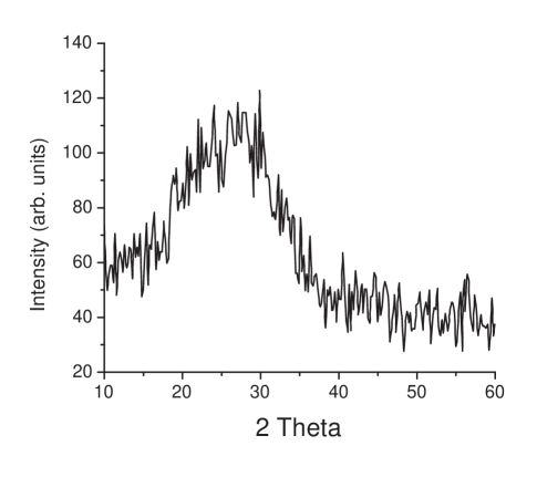
X-ray diffraction studies were done on all the samples. Without exception, all the samples, as-grown and heated, were amorphous in nature. Figure(1) illustrates the nature of diffractograms obtained. The small hump seen in the diffractogram is characteristic of the short range ordering present in films3.8 ; 3.9 . However, no peaks indicating the crystalline nature of were seen. This can be expected since the amount of material () for scattering the X-rays may not be sufficient. X-ray diffraction analysis hence proved futile in estimating nanocrystal’s size.
III.2 Surface Morphology studies
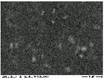
We have characterized all the samples for their morphology by Surface Electron Microscopy (SEM). We have displayed few representative SEM micro-graphs of samples whose thickness was in fig(3).
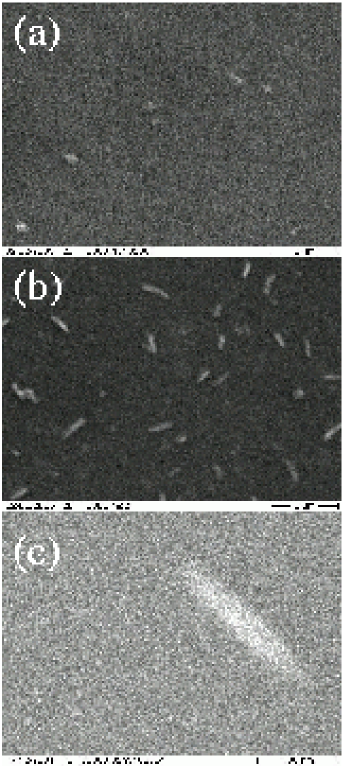
Morphological manifestations seem to be consistent with the structural studies, with the background of being featureless, indicating that the material is still in it’s amorphous state. However, sparsely distributed grains of are visible against this background. The possibility of grains being that of is over-ruled since it is known to exist in amorphous state on thermal evaporation at room temperature.
The SEM micrographs of all the as-grown films showed that they were having grains of two distinct morphologies. While grains of spherical shape is predominant in the as-grown sample (fig 2a), the second type of grains are spindle shaped. Though they are sparsely present in the as-grown sample, their number increases with heating. Fig(2b) exhibits a sample heated for 3 hours (the diffractogram of this sample is shown in fig 1). The simultaneous existence of both phases is evident. Further heating leads to a further increase in the population of the spindle shaped grains. The grain morphologies are similar to that observed and detailed in Pankaj’s workthesis . The average grain size of the spherical grains in the as-grown films was estimated from the SEM micrograph (fig 2a) and were found to be 430nm. The average grain size of this species is about 140nm in the sample heated to 3hrs. Similar estimation of grain size in the thicker sample (d=4000Å, see fig 3) gives the average spherical grain’s size as 220nm. Much variation was not seen in grain size in the 4000Å samples on heating upto 3 hours. No systematic variation in grain size was found with sample thickness.
A systematic study of the variation of grain size with heating time could not be done as samples heated for time greater than 3hrs showed no features on the surface. While one may infer to be absent in these samples, as can be seen from the next section, their existence in the film is beyond doubt. One can safely conclude, that the grains migrate/ diffuse into the film’s thickness away from the surface. It is difficult to comment on the grain size of the second species of grains due to it’s asymmetrical shape. While the average width of these spindle’s was found to be 140nm, the length of these grains varied from 400nm to . Spindle shaped nanocrystals are common and are characterized by the aspect ratio (length/width). The aspect ratio of the second species of grains was found to lie between 2.8 to 7.0 in the sample heated for 3 hours.
III.3 Optical properties of the samples
Visual examination of the films showed that it had a yellow to reddish-brown color depending on the thickness of the film. This is in keeping with the color of films of the corresponding thickness. On heating, the color of the films became darker with preceivable change in the film texture. We have studied the optical absorption of all the samples. Typical absorption spectrum of the samples is shown in fig(4) for the purpose of illustration. As expected the thicker film (d=4000Å, labeled ’a’) absorbs more strongly than the thinner film (sample labeled ’b’). Both and in film state do not strongly absorb in the wavelength region of 600-900nm and show characteristic fringes (maxima/ minima) in the same region. However, in these samples where is embedded in films, very strong absorption peaks are seen at 710nm and 820nm. These peaks are contributed by surface plasmons.
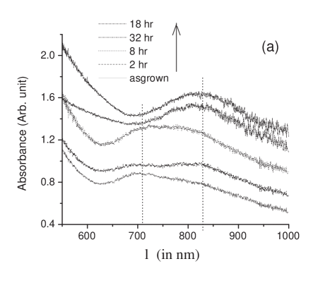
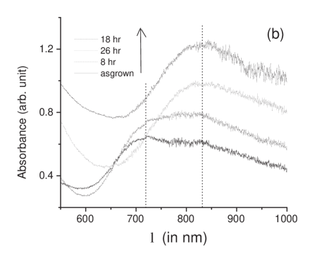
One can immediately ascribe the two peaks present in the UV-visible spectra to the two type of grains (spherical and spindle shaped) present in the film. Two factors help in associating a peak with each type of grain. Trivially, one can immediately correlate these spectra with the results of the SEM studies and identify the peak around 710nm with the spherical grains and the peak of 830nm to the spindle shaped grains. This inference was extrapolated from the variation seen in size with heating till three hours. The morphological studies showed that with heating the spherical grain’s number decreased while number of the spindle shaped grains increased. Recollect, it was concluded that on heating beyond three hours the grains migrated within the film’s thickness. Since SEM only investigates the sample’s surface, one can not conclusively justify this based on the morphological studies, however, since the optical studies were done in transmission mode the response is due to the film as a whole. Thus, even though grains were not visible in SEM micrographs, the absorption spectra show spherical grains to be present in the sample even after heating for eight hours. However, the diminishing peak at 710nm and increasing peak at 830nm suggests the spherical grains convert into spindle grains, thereby increasing the population of that grain.
Another reason to associate the 830nm peak to the spindle shaped nano-crystals is due to the nature of the peak itself. Observe the peak’s spread out to the longer wavelength. This results from the fact that the nanoparticles are spindle shaped having length (b) different from the width (a) or in other words an non-unity ( 1) aspect ratio (b/a). The spread into longer wavelength becomes greater for large aspect ratio.
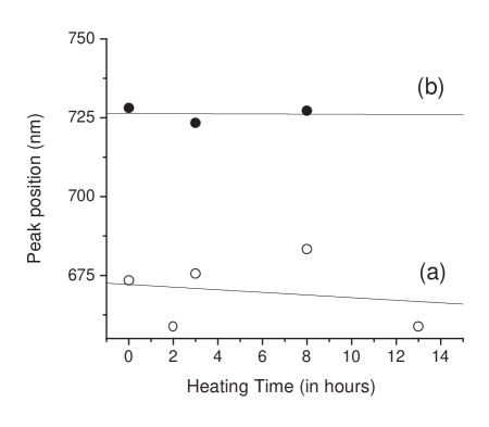
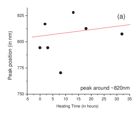
As can be seen the optical properties (SPR) of nanocrystals are also effected by the particle shape and size. Usually, the decrease in grain size is not justified by the decreasing peak size but by a blue-shift in the peak positionblue1 ; blue2 . This is due to the size dependence of the band gap in the quantum regime. To establish the peak positions, the broad peaks of the UV-visible spectra were deconvoluted into two Gaussian using the software ”Origin 6.0”. The variation in peak position with heating time is shown in fig(5). The points of these graphs are quite scattered and reflects the difficulty in uniquely identifying the peak position using the software due to the lack of sharp shoulders in the spectras. While there is a definite blue shift in the 710nm peaks, the peak positions of the 830nm increases (red-shifts) with heating. Converse to the blue shift which show decrease in nanocrystal’s size, the red shift suggests an increase in nanocrsytal size.
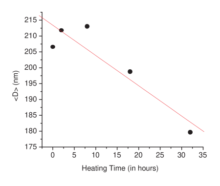
Qualitative estimation of the grain size can be made using the UV-visible spectra. It has been extensively used to determine the spherical metal nanocrystals size/diameter using the equation
where h is the Planck’s constant, is the full-width at half-maximum of the absorption peak and is the Fermi velocity of electrons. Liang-Fu Louwsbook gives the value of Fermi velocity to be around . Using this formula, the grain size was calculated as a function of heating duration. The decrease of grain size with heating time is shown in fig(6). Notice that the grain size thus estimated and that evaluated from SEM micrographs are in good agreement.
It would be worthwhile to recollect that films grown at higher deposition rates (2-5nm/sec) lead to films which crystallizes with nH structures (). On heating these structures convert into the stable 4H state. The diminishing 710nm peak and growing 830nm peak may relate to nH structures reducing to 4H. Since the dielectric constant of films with nH structure lies between 60-190 (all possible structures) and that of the stable 4H structured films is reported to be 15-30, one may conclude the two well resolved SPR peaks are due to the diverge dielectric constants of the nanocrystals.
IV Conclusion
Two peaks were found in the UV-visible absorption spectra of films which had nanocrystals embedded in them. The peaks are associated with two morphological grains each corresponding to a type of crystalline states of marked by different dielectric constants. The results of this experiments show that as the disparity between the material acting as the host and the material whose nanocrystals are suspended in it increases, there is a distinct blue-shift in the surface plasmon resonance (SPR).
Acknowledgement
The author would like to express his sincere gratitude to Dr. A. G. Vedeshwar, Department of Physics and Astrophysics, University of Delhi for allowing to use the facilities of his lab and Dr. N. C. Mehra, University Science and Instrumentation Center (USIC), University of Delhi, for carrying out the SEM analysis.
References
- (1) J. Z. Xu, Y. Zhang, G. X. Li and J. J. Zhu, Mater. Sci. Eng. C 24 (2004) 833.
- (2) T. W. H. Oates, L. Ryves, M. M. M. Bilek and D. R. McKenzie, Sensors Actuators B 109 (2005) 109.
- (3) A. Sreekumaran Nair, Renjis Tom and T. Pradeep, J. Environ. Monit. 5 (2003) 363.
- (4) A. Vaskelis, A. Jagminiene, L. Tamasaukaite-Tamasiunaite and R. Juskenas, Electrochim. Acta 50 (2005) 4586.
- (5) K. C. Krongman, T. Druffel and M. K. Sunkara, Nanotechnology 16 (2005) 5338.
- (6) H. Weller, Angew. Chem. Int. Edn. Engl., 32 (1993) 41.
- (7) H. H. Michael, M. Samuel, F. Henning, Q. Y. Hao, Y. W. Yi, K. Hannes, W. Eicke, R. Richard and D. Y. Pei, Science 292 (2001) 1897.
- (8) K. Naoi, Y. Ohko and T. Tatsuma, J. Am. Chem. Soc., 126 (2004) 3664.
- (9) S. Vijayalakshmi and H. Grebel, Handbook of Nanostructured Materials and Nanotechnology, ed H. S. Nalwa (Academic Press, NY 2001).
- (10) Taek-Soo Kim, Wei Sun, Chul-Jin Choi and Byong-Taek Lee, Rev. Adv. Mater. Sci., 5 (2003) 481.
- (11) V. Halte, J-Y Bigot, B. Palpant, M. Broyer, B. Prevel and A. Perev, Appl. Phys. Lett. 75, (1999) 3799.
- (12) A. I. Stepanov, D. E. Hole and P. D. Townsend, Nucl. Instrum. Methods Phys. Res. B, 882 (2000) 166.
- (13) A. A. Ismail, Appl. Catal. B, 58 (2005) 115.
- (14) M. A. Villegas, M. A. Garcia, S. E. Paje and J. LLopis, Mater. Res. Bull., 40 (2005) 1210.
- (15) E. Borsella, E. Cattaruzza, G. De Marchi, F. Gonella, G. Mattei, P. Mazzoldi, A. Quaranta, G. Battaglin and R. Polloni, J. Non-Cryst. Solids, 22 (1999) 245.
- (16) G. Mie, Ann. Phys., 25 (1908) 377.
- (17) H. C. van del Hulst, Light scattering by small particles (Dover, New York 1981).
- (18) A. Babapour, O. Akhavan, R. Azimirad and A. Z. Moshfegh, Nanotechnology, 17 (2006) 763.
- (19) D. Faccio, P. Di Trapani, E. Borsella, F. Gonella, P. Mazzoldi and A. M. Malvezzi, Europhys. Lett, 43, (1998) 213.
- (20) S. Dhara, S. Chandra, P. Magudapathy, S. Kalavathi. B.K. Panigrahi, K. G. M. Nair, V.S. Sastry, C.W. Hsu, C.T. Wu, K.H. Chen, and L.C. Chen, J. Chem. Phys., 121 (2004) 12595.
- (21) P. Gangopadhyay, P. Magudapathy, R.Kesavamoorthy, B. K. Panigrahi, K. G. M. Nair and P. V. Satyam, Chem. Phys. Lett., 388 (2004) 416.
- (22) Xiao-Dong Feng, Min-Bo Tian and Zheng-Xin Liu, J. Vac. Sci. Tech. B, 16, (1998) 2934.
- (23) F. Ren, C. Z. Jiang, C. Liu, D. J. Fu, Y. Shi, Solid State Commun., 135 (2005) 268.
- (24) R. Lopez, T. E. Haynes, L. A. Boatner, L. C. Feldman and R. F. Haglund Jr., Appl. Phys. Letters, 79 (2001) 3161.
- (25) Xiaofeng Lu, Linlin Li, Wanjin Zhang and Ce Wang, Nanotechnology 16, (2005) 2233.
- (26) D. O. Henderson, A. Ueda, Y-S Tung, R. Mu, W. C. White, R. A. Zuhr and Jane G. Zhu, J. Phys. D. Appl. Phys., 30 (1997) 1432.
- (27) Xavier Cartoixa and Lin-Wang Wang, Phys. Rev. Lett., 94 (2005) 236804.
- (28) P. Arun and A. G. Vedeshwar, J. Appl. Phys., 79, (1996) 4029-37.
- (29) P. Arun and A. G. Vedeshwar, J. Mater. Sci., 31, (1996) 6507-10.
- (30) P. Arun, A. G. Vedeshwar and N. C. Mehra, Mater. Res. Bull. (USA) 32, (1997) 907-13.
- (31) P. Arun and A. G. Vedeshwar, J. Non-Cryst. Solids, 220, (1997) 63-68.
- (32) P. Arun and A. G. Vedeshwar, J. Appl. Phys. D. (UK), 32, (1999) 183-190.
- (33) Pankaj Tyagi and A. G. Vedeshwar, Phys. Rev. B 63, 245315 (2001).
- (34) Pankaj Tyagi, A. G. Vedeshwar and N. C. Mehra, Physica B 304, 166 (2001).
- (35) Pankaj Tyagi and A. G. Vedeshwar, Bull. Mater. Sci. 24, 297 (2001).
- (36) Pankaj Tyagi and A. G. Vedeshwar, Phys. Stat. Sol. (A).
- (37) R. S. Rawat, P. Arun, A. G. Vedeshwar, P. Lee and S. Lee, J. Appl. Phys., 95, 7725-30 (2004).
- (38) L. Cervinka and A. Hurby, J. Non-Cryst. Solids, 48 (1982) 231.
- (39) V. V. Killedar, C. D. Lokhande and C. H. Bhosale, Indian J. Pure Appl. Phys., 36 (1998) 33.
- (40) V. V. Killedar, C. D. Lokhande and C. H. Bhosale, Mater. Chem. Phys., 47 (1997) 104.
- (41) B. B. Nayak, H. N. Acharya, Thin Solid Films 122, (1984) 93.
- (42) I. K. El Zawawi, A. Abdel-Moez, M. A. Riad and M. Mounir, Thin Solid Films 324, (1998) 300.
- (43) I. K. El Zawawi, A. Abdel-Moez, M. A. Riad and M. Mounir, Phys. Low-Dim Struct. 7/8, (1998) 155.
- (44) N. S. Yesugade, C. D. Lokhande and C. H. Bhosale, Thin Solid Films, 263 (1995) 145.
- (45) A. G. Vedeshwar, J. Phys. III (France), 5 (1995) 1161.
- (46) A. M. Farid and A. E. Bekhut, Vacuum 59 (2000) 932.
- (47) G. C. Trigunayat, Solid State Ionics 48, 3 (1991).
- (48) R. Coehoorn, G. A. Sawatzky, C. Haas and R. A. deGroot, Phys. Rev. B, bf 31 (1985) 6739.
- (49) A. M. Fernandez and O. N. Srivastava, J. Appl. Cryst 10 (1977) 32.
- (50) L. V. Poretskaya, L. E. Shelimova and E. V. Skudnova, ”Semiconducting II-VI, IV-VI, and V-VI compounds”, (Plenum, NY 1969).
- (51) G. Dalba, P. Fornasini, G. Giuta, Solid State Commun., 62,(1987) 773.
- (52) P. Arun and A. G. Vedeshwar, J. Mater. Sci. 31, (1996) 6507.
- (53) Pankaj Tyagis’s PhD thesis, ”Optical properties of Group IIB iodide ( , and ) films”, University of Delhi 2001.
- (54) J-T Lue, J. Phys. Chem. Solids, bf 62 (2001) 1599.
- (55) W. Li, S. Seal, E. Megan, J. Ramsdell, K. Scammon, G. Lelong, L. Lachal, K. A. Richardson and K. Scammon, J. Appl. Phys., 93 (2003) 9553.
- (56) Liang-Fu Lou, ”Introduction to Phonons and Electrons”, World Scientific, Singapore (2003), pg 138.