Observation of a Mott insulating ground state for Sn/Ge(111) at low temperature
Abstract
We report an investigation on the properties of 0.33 ML of Sn on Ge(111) at temperatures down to 5 K. Low-energy electron diffraction and scanning tunneling microscopy show that the phase formed at 200 K, reverts to a new R30∘ phase below 30 K. The vertical distortion characteristic of the phase is lost across the phase transition. Angle-resolved photoemission experiments show that concomitantly with the structural phase transition, a metal-insulator phase transition takes place. In agreement with theoretical predictions, the R30∘ ground state is interpreted as the experimental realization of a Mott insulator for a narrow half-filled band in a two-dimensional triangular lattice.
pacs:
68.18.Jk 79.60.-i 68.37.EfThe band theory of crystalline solids is one of the most successful parts of solid state physics. However, exceptions to the predictions of simple band theory are found when the approximation of independent electrons fails, due to electron repulsion effects Gebhard . This is the case of insulating materials that should be metallic according to band theory. In a simple view, the independent electron approach is not adequate when the kinetic energy (band width) is smaller than the electron-electron interaction (Coulomb energy). The new ground state formed is the so-called Mott insulator Gebhard . It is characterized by strong electron-electron interactions, which are crucial to understand the behavior of many interesting materials Imada_Capone_Jerome .
Semiconductor surfaces present narrow surface bands, and thus are excellent playgrounds to search for Mott insulating phases, and to understand their rich physical behavior. Known examples of Mott insulators of this kind include the surfaces of SiC(0001) SiC and of K/Si(111):B WeiteringPRL . In both cases, the occupation with adatoms of sites produces a R30∘ structure ( in the following), which should exhibit a half-filled surface band, but is indeed insulating. The reconstructions of 0.33 monolayers (ML) of group IV adatoms on Si(111) or Ge(111) are isoelectronic with these systems and also exhibit the same atomic arrangement. Thus, they are good candidates to observe the same kind of behavior FloresPSS ; SantoroPRB . However, at variance with the two cases described above, the structure for both Sn and Pb on Ge(111) below 200 K is a reconstruction Carpinelli ; FloresrevJPCM . This phase is metallic AvilaPRL ; UhrbergPRL . The unit cell is distorted in a vertical direction because it contains three Sn adatoms and one of them is at a position higher (“up”) than the other two (“down”). The different behavior in isoelectronic systems with such a similar atomic arrangement (Mott insulating vs. metallic state), raises exciting issues on the origin of the different ground states found.
In this Letter, we demonstrate that the ground state of Sn/Ge(111) is a Mott insulating phase of symmetry. We provide a full description of its structural and electronic properties by measuring at temperatures well below the values reached before. We find that below 30 K, the phase becomes unstable and a new phase of symmetry notaroot3RTLT is formed. The phase transition is fully reversible, and it is due to the disappearance of the vertical distortion at low temperatures. Concomitantly with the structural phase transition, a band gap opens in the low-temperature, flat phase. The Mott insulating phase competes with a metallic, -distorted state, which is more stable at higher temperatures.
The experiments were carried out in two different ultra-high vacuum chambers, and include angle-resolved photoemission spectroscopy (ARPES), low-energy electron diffraction (LEED), and scanning tunneling microscopy (STM) measurements of 0.33 ML of Sn atoms on Ge(111). These techniques provide complementary information on both the short-range (STM) and long-range (LEED) surface order, and on the electronic structure and the single-particle spectral function (ARPES). The STM apparatus was a low temperature microscope (Omicron), which operated between 4.7 and 300 K. STM images and height profiles shown are neither filtered nor treated, with the exception of the subtraction of a plane. ARPES experiments down to 10 K used a Scienta SES-2002 electron analyzer and synchrotron light from the SIS beamline at the Swiss Light Source resolution . Both chambers were equipped with LEED. The substrate was -type Ge(111) ( =0.4 cm). The preparation of the sample and of the phase have been described before AvilaPRL .
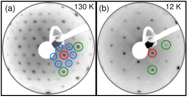
A sharp LEED pattern is observed at 130 K (Fig. 1). Below 30 K, the superstructure spots weaken and the pattern becomes . The new pattern is also sharp and with low background. The phase transition is fully reversible. We refer to this new phase as low-temperature (LT-) notaroot3RTLT .
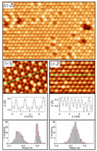
Fig.2 shows filled-states representative STM images for the LT- phase. There is an excellent long range order, and only atoms around defects appear brighter, indicating a local pinning to a symmetry. To make easier the comparison between the two phases, images of the same size of a LT- and surface are also shown. In the latter the larger protrusions correspond to the “up” atom of the reconstruction, and form a hexagonal pattern. The two “down” atoms are resolved and imaged as smaller protrusions.
In order to understand the nature of the LT- phase, the first step is discarding any artifact in the STM images. Such effects have been reported for the low temperature reconstructions of Si(100)YoshidaSi100PRB , Ge(111) RiederGe111PRB , and Pb/Ge(111) BrihuegaPbGePRL . In agreement with previous studies on Ge(111) with a similar doping as our sample RiederGe111PRB , we find tip-induced band bending effects when the sample is in depletion conditions (i.e. positive sample voltage for our -doped sample). For negative sample voltages, images were acquired for a variety of measuring conditions. We find no detectable effect of the tip for a range of voltages and tunneling current, from which we select a safe range of reliable measuring conditions of V and nA. In conclusion, the loss of long range order observed in LEED is explained from the disappearance of the atomic vertical distortion of the phase, as observed in STM images. These structural modifications are fully reversible going up and down with temperature. Thus, the structure of the LT- phase corresponds to the occupation of equivalent sites.
This finding is analyzed quantitatively in Fig. 2, which shows a height analysis for both the and the LT phases. Atomic heights are measured for both reconstructions for 250 and 350 atoms, respectively. The results are shown as histograms in Fig. 2. Two different, well defined heights are found for the phase. The height difference is 0.65 Å. The height distribution is fit using two gaussian functions. The height of “up” atoms is taken as zero level. An analogous height analysis for the LT- phase shows that there is a single atomic height, following a gaussian distribution. As mentioned above, atoms at distorted “up” positions survive around defects also for the LT- phase. The location and relative height of these atoms has been monitored across the phase transition. We find that their atomic height does not change, and that they become part of the reconstruction, once the phase transition is completed. Thus, their atomic height can be used to compare the atomic heights found for the LT- and the phases. Using this method, we find that the atomic height corresponding to the LT- phase is 0.35 Å, between the heights of the “up” and “down” atoms of the phase.
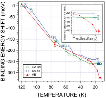
A crucial point to understand the nature of the LT- phase is to analyze its electronic structure with ARPES. When ARPES is used to probe metal/semiconductor interfaces, surface photovoltage effects should be taken into account DemuthPRL . UV radiation stabilizes a temperature-dependent surface photovoltage, which shifts uniformly both the core levels binding energies and the valence band. As expected for an -doped sample, the three binding energies probed (Ge 4d, Sn 3d and valence band) shift at low temperature to smaller values (Fig. 3). The saturation of the shift at 30 K for Ge 4d and Sn 3d indicates that “flat band conditions” are reached notaSPV1 . This situation corresponds to a complete elimination of the band bending EGMPRB . For temperatures below K, the binding energy of the valence band leading edge deviates from the behavior of the core levels. The energy difference below 15 K is 60 meV. This differential shift is attributed to the opening of a surface band gap notaSPV2 .
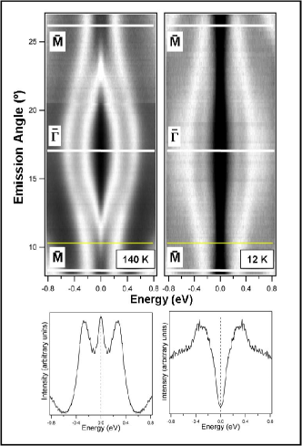
The opening of a surface band gap is confirmed by a detailed analysis with ARPES. Fig. 4 shows the valence band along direction, which corresponds to , for two different surface temperatures. The data are symmetrized with respect to the Fermi energy following standard practice in ARPES work on the cuprates cuprates . In the symmetrized data, the effect of the Fermi function on the temperature dependence of the spectral function is removed. The position of the Fermi energy is corrected by the surface photovoltage, measured from the uniform shift of the Ge 4d and Sn 3d core levels. The Fermi energy thus determined is in perfect agreement with the Fermi edge observed in the metallic phase. The same method is used to determine the Fermi energy in the LT- phase. Note the two surface state bands observed in the phase, one of them crossing the Fermi energy. The spectral weight closer to the Fermi energy in the phase, disappears in the LT- phase, indicating the opening of a surface band gap (Fig. 4). The redistribution of spectral intensity around the Fermi energy affects a range of 0.4 eV below the valence band leading edge. Indeed, the surface state which crossed the Fermi energy in the phase is strongly depleted. These change are again fully reversible with temperature.
As shown in Fig. 4, the band gap and the corresponding redistribution of spectral intensity is fairly uniform, and it affects extended areas of reciprocal space. This is typical of a Mott insulator, where the band gap is not related to the surface periodicity but rather to electron repulsion. All these features of the electronic structure are qualitatively consistent with the spectral changes expected for a Mott transition Imada_Capone_Jerome ; PerfettiPRL ; ZhangPRL . The stabilization of a charge density wave by the Peierls mechanism would also give rise to a gap opening. However, this possibility can be safely excluded, first because the value of the gap is much larger than the thermal energy at the critical temperature (k), and second because the gap affects extended areas of reciprocal space and is not related to any nesting vector GrunerCDW .
The observation of a Mott insulating ground state is understood from theoretical calculations performed in the local-density approximation (LDA), which have compared the stability of a flat vs. a distorted structure. The ground state found was the phase AvilaPRL , but the energy difference with respect to a flat phase was only 5 meV/Sn atom FloresPSS . If electron correlation effects are considered, the energy difference between both phases would be even smaller, and close to the accuracy of the calculation. It was also predicted that a flat phase should become a Mott insulator FloresPSS . The experiments show that both states are indeed observed. The energetic balance favors the distorted metallic state above 30 K, while the insulating, flat phase is observed below this temperature. The existence of a phase transition indicates that there is a temperature dependent modification of the potential energy landscape. The stability of the phase lies on a delicate balance between the electronic energy gained in the new structure and the elastic energy involved in the distortion FariasPRL , which affects not only the Sn atoms, but also several layers of the Ge(111) crystal MascaraquePRL . The elastic response of the lattice is effectively modified in Ge at low temperatures, as demonstrated by the negative lattice expansion and anomalous Grüneisen parameters below K Cowley . This modification is due to a change of the phonon modes excited Scheffler . On the other hand, we may expect that the charge screening is also modified at very low temperatures due to the decrease of the carrier concentration, favoring an increase of the effective electron repulsion. Any of these two effects may be strong enough to provoke the phase transition. Further theoretical work is needed to completely solve this question. Note that recent reports provide contradictory evidence on the existence of a glassy-like ground state for Pb/Ge(111) at low temperatures PlummerPbGePRL ; BrihuegaPbGePRL . This disordered state is different from the phase that we report here, which represents a well-ordered structure associated to a metal/insulator transition.
In conclusion, we present experimental evidence for a Mott insulating ground state of Sn/Ge(111). The results of three techniques (LEED, STM, and ARPES), which probe very different surface properties, converge to show that a structural phase transition from a distorted and metallic phase to a flat and insulating LT- phase is observed at 25 K. This finding is an indication of a more general phenomenon, which may also be observed in different metal/semiconductor interfaces.
We acknowledge financial support from MCyT (Spain) under grants MAT2003-08627-C0201 and FIS2005-0747. A.M. thanks the program “Ramón y Cajal”. R.C. thanks “Comunidad de Madrid” and “Fondo Social Europeo”. Part of this work was performed at the Swiss Light Source, Paul Scherrer Institut, Villigen, Switzerland.
References
- (1) F. Gebhard, The Mott metal-insulator transition (Springer, New York, 1997).
- (2) M. Imada, A. Fujimori, and Y. Tokura, Rev. Mod. Phys. 70, 1039 (1998); M. Capone et al, Phys. Rev. Lett. 93, 047001 (2004); P. Limelette et al, Science 302, 89 (2003).
- (3) L.I. Johansson, F.Owman, and P. Mårtensson, Surf. Sci. 360, L478 (1996); J.-M. Themlin et al, Europhys. Lett. 39, 61 (1997).
- (4) H.H. Weitering et al, Phys. Rev. Lett. 78, 1331 (1997).
- (5) F. Flores et al. Prog. Surf. Sci. 67, 299 (2001).
- (6) G. Santoro, S. Scandolo and E. Tosatti, Phys. Rev. B 59, 1891 (1999).
- (7) J.M. Carpinelli et al, Nature 381, 398 (1996) and Phys. Rev. Lett. 79, 2859 (1997).
- (8) J. Ortega, R. Pérez, and F. Flores, J. Phys. Condens. Matter 14, 5979 (2002) and references therein.
- (9) J. Avila et al, Phys. Rev. Lett. 82, 442 (1999).
- (10) R.I.G. Uhrberg and T. Balasubramanian, Phys. Rev. Lett. 81, 2108 (1998).
- (11) A R30∘ phase is also observed at room temperature, due to excitation of vertical dynamical fluctuations in the distorted structure.
- (12) The energy/angle resolution is 9 meV/0.1∘.
- (13) S. Yoshida et al., Phys. Rev. B 70, 235411 (2004) and references therein.
- (14) R.M. Feenstra et al, Phys. Rev. B 71, 125316 (2005).
- (15) I. Brihuega et al., Phys. Rev. Lett. 95, 205102 (2005).
- (16) J.E. Demuth et al. Phys. Rev. Lett. 56, 1408 (1986); M. Alonso, R. Cimino, and K. Horn, Phys. Rev. Lett. 64, 1947 (1990).
- (17) The shift observed at 30 K is the maximum total shift expected, as estimated from sample doping and the change of the chemical potential and of the Ge band gap with temperature.
- (18) E.G. Michel et al. Phys. Rev. B 45, 11811 (1992).
- (19) A larger photovoltage for the valence band is discarded, first because the shift detected exceeds the maximum value due to a change of the band bending only, and second because the photon flux used for probing the core levels is larger than for the valence band.
- (20) A. Damascelli, Z. Hussain, and Z.X. Shen, Rev. Mod. Phys. 75, 473 (2003).
- (21) L. Perfetti et al, Phys. Rev. Lett. 90, 166401 (2003).
- (22) X.Y. Zhang, M.J. Rozenberg, and G. Kotliar, Phys. Rev. Lett. 70, 1666 (1993).
- (23) G. Grüner, Density Waves in Solids (Addison-Wesley, Reading, MA, 1994).
- (24) D. Farias et al, Phys. Rev. Lett. 91, 016103 (2003)
- (25) A. Mascaraque et al, Phys. Rev. Lett. 82, 2524 (1999).
- (26) G. Dolling and R.A. Cowley, Proc. Phys. Soc. 88, 463 (1966).
- (27) S. Biernacki and M. Scheffler, Phys. Rev. Lett. 63, 290 (1989).
- (28) J. Guo, J. Shi, and E.W. Plummer, Phys. Rev. Lett. 94, 036105 (2005).