Monte Carlo approach of the islanding of polycrystalline thin films
Abstract
We computed by a Monte Carlo method derived from the Solid on Solid model, the evolution of a polycrystalline thin film deposited on a substrate during thermal treatment. Two types of substrates have been studied: a single crystalline substrate with no defects and a single crystalline substrate with defects. We obtain islands which are either flat (i.e. with a height which does not overcome a given value) or grow in height like narrow towers. A good agreement was found regarding the morphology of numerical nanoislands at equilibrium, deduced from our model, and experimental nanoislands resulting from the fragmentation of YSZ thin films after thermal treatment.
pacs:
87.53.Wz, 68.55.Jk, 68.60.DvI Introduction
In recent years, the formation of mesoscopic structures on crystal surfaces has become a subject of intense experimental and theoretical study. Generally, for non periodically ordered nanostructures, the increasing specific area is favorable in order to enhance the physical properties (in optics, semiconducting etc) owing to the increased number of active sites shalaev .
We will study here the evolution of a thin film deposited on a single crystalline substrate with or without defects. The thin film itself is polycrystalline with the size of crystals corresponding to the thin film thickness. The method employed experimentally to obtain such thin films is the sol gel processing brinker . The sol gel method proceeds as follows: a thin film is deposited on the substrate by dip coating. After a first heat treatment (stage I), the thin film of nanometric thickness is made of a large amount of nanocrystals of random orientation. At this stage the film thickness is much larger than the mean size of these nanocrystals. After a second heat treatment at higher temperature (stage II), thermal annealing induces grain growth. At this stage, the size of the crystals is of the order of the film thickness. Simultaneously, the film is submitted to fragmentation into more or less interconnected islands in order to reduce the total energy and hence to reach a more stable state miller .
The aim of this article if to model the formation of nanoislands after thermal annealing of polycrystalline nanometric thin films with no deposition. Much literature has been written on models of the origin of islands in homoepitaxial or heteroepitaxial single crystalline thin films shchukin ; golovin ; tekalign ; spencer ; spencer2 ; eisenberg ; zhang . Less model exist on nanoislands which form spontaneously without deposition tekalign ; olivi ; olivi2 . In this last case, surface roughening caused by the intrinsic elastic strain and lattice mismatch between the thin film and the substrate has been widely experimentally studied gao ; jonsdottir . Theoretical studies showed that due to morphological variations in the shape of the surface an originally flat film surface of a stressed solid thin film is unstable spencer3 ; freund . Experiments showed that film roughening under various conditions and surface morphology form islands eaglesham ; snyder ; tersoff , undulating surfaces yao ; pidduck and cusped surfaces jesson .
Up to now most of the numerical and theoretical models (cited above) which represent the evolution of a nanometric thin film are models which employ a continuous representation of the elasticity of the thin film and of the mismatches between the film and the substrate. Moreover, only a few articles deal with numerical model which take into account polycrystalline thin films olivi ; olivi2 . The question is: is it possible to model the evolution of nanometric thin films and nanometric islands with a continuous representation of their elasticity and of the intrinsic strain resulting from lattice mismatches between the film and the substrate? To avoid this question, we used a Monte Carlo method applied to a non continuous representation of a polycrystalline thin film. This model is derived from the Solid on Solid model but is applied here in the absence of deposition. Our model is also derived from the two dimensional models of polycrystalline materials which computed the evolution of polycrystalline domains during thermal treatments srolo1 ; srolo2 ; srolo3 . Our model is based on energetic considerations: we compute the energies resulting from the elastic strains due to surface morphology of the thin film, the lattice mismatches and the grain boundary energies. We will see that the resulting shapes of the islands depend on the relative values of these three energies.
In section II, we shall present the model. In section III, results are shown and discussed in the light of experimental results. Section IV corresponds to the conclusion.
II Numerical procedure
We modelled a thin polycrystalline film deposited on a single crystalline substrate either perfect or with a random distribution of defects.
Our model represents a thin film of thickness. Each domain contains approximatively 500 to 1000 atoms.
In the case of a substrate with no defects, the domains have a square horizontal section. The thin film is then represented by a square lattice of domains with periodic boundary conditions. This model represents an polycrystalline thin film deposited on a single crystalline substrate with no defects.
In the case of a substrate with a random distribution of defects, the domains have a section depending on the distribution of defects. The defects are representative of the local maximum value of stress intrinsic to the substrate. The locations of these stresses are obtained by generating a random array of domains. Each domain is then corresponding to a local maximum value of the stress in the substrate at the location of the domain. The locations of the domains do not change during computation: no displacements of the stress maxima are occurring in the substrate. Hence the geometries of the domains correspond to the Voronoi array of the distribution of defects. This model represents a polycrystalline thin film deposited on a single crystalline substrate with defects like dislocations, disinclinations and planar defects.
The mechanism of mass transport during thermal annealing is surface diffusion:
| (1) |
where is the transported number of atoms per unit time and is the height difference in thin film thickness, for changes in the surface occurring during the mass transport of volume jullien .
The flux may be also written jullien :
| (2) |
where is the surface curvature, is the surface diffusion constant, is the surface tension, is the characteristic volume entering surface diffusion, is the Boltzmann constant and is the absolute temperature. In terms of the characteristic measures in the system we obtain:
| (3) |
where is the characteristic mean size of the domains and is the difference of heights for two locations at a distance . Similarly, in terms of characteristic measures, equation (1) yields:
| (4) |
for one time interval and for . Finally, relating equations (3) and (4) holds:
| (5) |
Hence, if we assume that the stress tensor inside the thin film is diagonal (for example for cubic phase thin films) the energy related to using the work of elastic forces, the Young modulus and the Poisson ratio is:
| (6) |
where is the displacement in the normal direction of the thin film for a time interval and is the displacement in horizontal direction related to the Poisson ratio .
If we deal with crystallographic orientations, let us report the behavior of single crystalline grain growth srolo1 where the driving force for change in the crystallographic orientation is related to the difference in pressure:
| (7) |
where is the sphere equivalent radius of the domain , is grain boundary surface tension and is the pressure. Several domains with the same crystallographic orientation may form the same grain. Hence, the growth of one grain is equivalent to the changes in crystallographic orientation of its neighbouring domains. If we use the characteristic measures of the system, with equation (7), we obtain the energy necessary to change the crystallographic orientation of one domain by calculating the work of the driving force deduced from the pressure:
| (8) |
where is the change in crystallographic orientation in the dimension of a length, associated to the work of the driving force given by equation (7).
Straightforwardly, we consider here three aspects which contribute to the energy of our thin film consisting of crystal species: the grain boundary energy (which is here equivalent to the interfacial energy between two elementary domains of different crystallographic orientations), the interfacial energy (which corresponds to the difference of energy between one elementary domain and the substrate) and the surface energy (which is related here to the height of each elementary domain). For our system of lattice domains, the energy necessary to change crystallographic orientation and height for domain with respect to domain becomes:
| (9) |
here is the height of elementary domain , is the coordinate of the crystallographic orientation in direct space on the horizontal plane, is the coordinate of the crystallographic orientation in direct space on the vertical plane, is the horizontal dimension of domain . The first and second terms of right hand side of the equality correspond to the interfacial energy coming from the grain boundary energy and from the energy with respect to the substrate. And the third term corresponds to the surface energy related to the heights of the domains (see equation (6)).
is the nearest neighbours number of a lattice domain. scales the interfacial energy between two elementary domains and is the boundary surface tension. scales the interfacial energy with respect to the substrate where is the interfacial surface tension of the domains with respect to the substrate. scales the surface energy obtained for different heights of the elementary domains. The values of and range from the upper value of orientation in horizontal and vertical planes respectively and have the dimension of a length. The time interval is chosen to be constant.
For Monte Carlo simulations of single phase films, only one type of event, namely lattice domain reorientation, was considered srolo1 ; srolo2 ; srolo3 . In our model, the height of each elementary domain is also submitted to changes like in the SOS model. But, unlike traditional SOS models, a species at domain may change its orientation with respect of its nearest neighbour and of the substrate.
In our model, each domain owns three states . has its value ranging from 0 to a value that depends on the physical properties of the thin film as will be seen in the results.
To simulate the islanding of our thin film, prior to simulation, all elementary domains were assumed to have a height of 1 and a random crystallographic orientation. After such initialization, the Monte Carlo algorithm works according to the classical Metropolis scheme metro . A lattice domain is chosen at random for three events (changes in the projections of the crystallographic orientation and height exchange) occurring. A neighbour of this domain is also chosen at random, and the energy given by equation (9) is computed.
The probability for each event is given by in which , where and are energies given by eq.(2), of the present configuration and the configuration which the system may reach respectively:
| (10) | |||
| (11) |
where is the Boltzmann constant and is the simulation temperature. Note that, as height exchange and crystallographic reorientation are not independent events, it may occur that a domain changes its height inducing a change in the orientational energy of the domain. Moreover, we used a Monte Carlo technique to study the statistical sampling of the thin film geometry, due to its surface topology. The values of , and may vary as well as the absolute temperature .
III Results
We computed all the results presented in the following figures at a temperature which correspond to experimental data (see below). The values of and are enclosed between 0.5 and 2.5. At the numerical thin film is perfectly flat and is thick i.e. all domains have the same height . Numerical results have been averaged over 5 runs. All the thin films are represented by a square of edge equal to 100 divided in 10000 domains with periodic boundary conditions. For the square lattice, each domain is 1 wide. For the random array, the domains are randomly distributed.
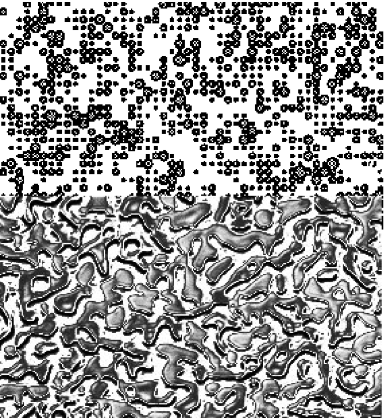
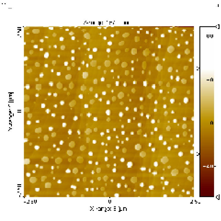
In figure 1, top image, one can see the resulting fragmentation of a thin film deposited on a square lattice. This figure is obtained after . The image on the bottom of figure 1 corresponds to a zirconia thin film after thermal annealing at 1500. This experimental thin film has been deposited by a sol gel process (introduced in section I) on a perfect single crystalline substrate of .
III.1 Crystallographic orientations and heights of the domains
We performed the Monte Carlo process as written in section II, for the two kinds of substrate i.e. with or without defects.
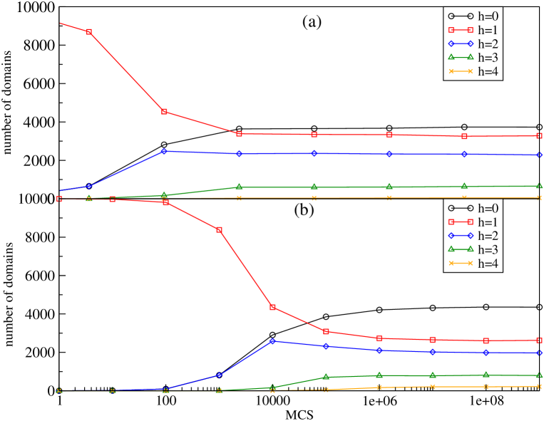
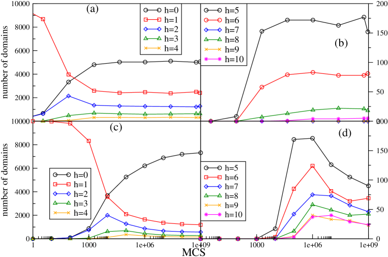
In figure 2a, one can see the evolution of the heights of the domains as a function of MCS, for , and , in the case of a periodic (square) array of domains Figure 2b corresponds to the same evolution with the same numerical values of and but for a random array of domains. One may see as in these two figures that the number of domains with heights increases until equilibrium is reached. During the same time, the numbers of domains with heights and 4 increase until reaching equilibrium at . There is a difference in the two figures for the number of domains with height : for a periodic array of domains this number is lower than for a random array of domains. This allows us to say that defects on the substrate lead to a larger dewetting of the thin film. We will see below that, depending on the values of and this dewetting may vary.
Figure 3a and 3b is the evolution of the orientations and as a function of MCS, for , and , in the case of a periodic (square) array of domains, where and vary from 0.5 to 2.5. Figure 3c and 3d corresponds to the evolution of the orientations and as a function of MCS, for , and , in the case of a random array of domains and for the same range of and . In figure 3a and 3b, we see that all domains (for a periodic array of domains) change from a random distribution of crystallographic orientations to the heteroepitaxial crystallographic orientation. Indeed, all domains for the two types of substrates get the lowest crystallographic orientation regarding its energy for on. In figure 3c and 3d we see that not all domains have reached the lowest crystallographic orientation with respect to their energy when there are defects on the substrate (for a random array of domains).
III.2 Influence of factors and
In this section, we will study the influence of the numerical values of and on the evolution of the heights of the domains and of the orientations of the domains as a function of MCS.
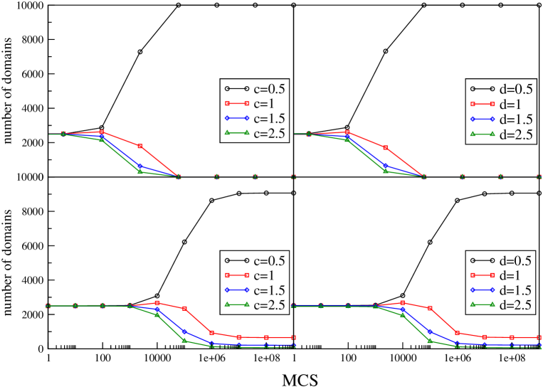
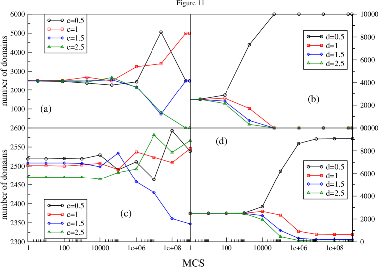
In figure 4 the evolution of the crystallographic orientations and are plotted as a function of MCS for , and for a square array of domains (resp. for a random array of domains). This figure corresponds to an average over 5 runs. The evolution of is clearly different for these values of and from the results obtained in figure 3, as well for a square array of domains as for a random array of domains.
We may say that the influence of the value of the constant is the same as for as these two constant are symmetrical and may be exchanged in equation (9).
In figure 5 the evolution of the heights as a function of MCS is shown for , and for a square array of domains (figure 5a and 5b) and for a random array of domains (figures 5c and 5d). Figure 5 show the evolution of the number of domains with heights ranging from to for the two kinds of substrates. The evolution of the number of domains with heights ranging from to shows that dewetting is larger and faster. The numbers of domains of heights ranging from to increase until reaching an equilibrium for .
III.3 Comparison with experiments
Yttria Stabilized Zirconia (YSZ) thin films were elaborated by sol-gel dip-coating. First of all, clear homogeneous sols were prepared from zirconium n-propoxide, acetylacetone and n-propanol. Yttrium nitrate () dissolved in n-propanol was used as the precursor. The yttria content was set to 10 mol so that YSZ is expected to crystallize in its cubic phase. A continuous amorphous film is realized by dip-coating after the setting of the zirconium n-propoxide concentration into the precursor solution equal to . The dipping speed was fixed to . These parameters allow to control the thickness of the continuous films which is close to in that case. The thickness was chosen to be small in order to maximize the interfacial effects. A primary thermal treatment at induces the crystallization of the films which is made of randomly oriented nanocrystals of zirconia. Finally, a last thermal treatment at high temperature (15 at ) induces an abnormal grain growth driven by the interface that leads to the epitaxy of the thin films. Finally, a last thermal treatment at high temperature (15 at ) induces the breaking up of the film and the formation of epitaxial YSZ islands. YSZ is in the cubic phase.
The c-cut saphire substrate was roughly polished in order to create defects. The roughly mechanico-chemical polishing was realized with colloidal silica dispersed into an acid solution. A short thermal treatment at high temperature (set to 15 at 1500) was necessary to get rid of high residual polishing-induced strains and to perform a very small mosaicity allowing the epitaxy of the thin film.
The experimental values of the parameters are, for comparison with numerical results : , ridder , pascal , , and for 1000 atoms per domain and is of the order of . We can consider that, as YSZ is in the cubic phase at room temperature, the value of parameter does not change with orientation due to quasi isotropy. For example, the data in literature only give an error of 20 % on the value of for all orientations pascal . The values of and are of the same order as .
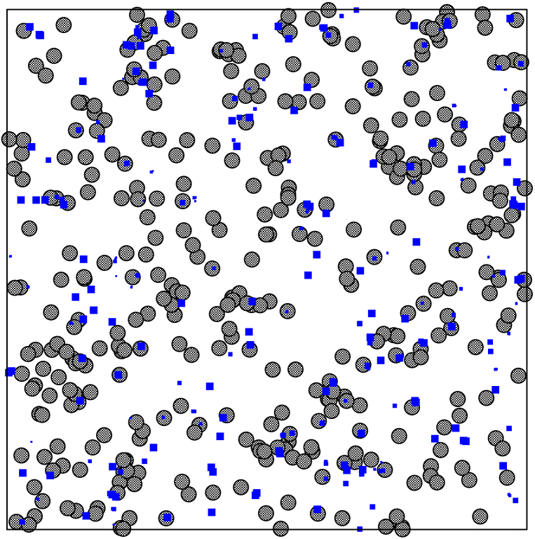
We compared a top view of an experimental thin film with a top view of a numerical thin film. Figure 6 is the top view of an experimental YSZ thin film on a c-cut sapphire substrate with defects. These experimental defects have been obtained by rough mechanical-chemical polishing. Figure 7 is a top view of a fragmented numerical thin film on a substrate with defects for the numerical values of corresponding to the experimental parameters. The grey disks correspond to islands of height, the dark squares correspond to higher islands with a size inversely proportional to their height.
IV Discussion
For the value and , the resulting evolutions of either the crystallographic orientations or the heights reach an equilibrium after (see figures 2 and 3).
In the case of crystallographic orientations, almost all and reach the minimum value of the four values which existed at . This means that the thin film is heteroepitaxial at equilibrium. More precisely, the vertical projection of the orientation in direct space reaches its minimum value with respect to the substrate and the horizontal projection of the same orientation also tends to minimize its value with respect to the orientation of its neighbouring domains. This is a phenomenon of minimization of the energy due to crystallographic mismatches: for small mismatches the energy is lower.
Let us analyze figure 4. In this case , while and . The horizontal projection of the crystallographic orientations in direct space depends on the initial configuration of the different horizontal crystallographic orientations. As is very low, it induces a low energy corresponding to the crystallographic orientation. So depending on the relative numbers of the different values of and as the value of the probability of values exchanges is close to 1 for each MCS, the resulting behavior of the number of relative values of follows a random behavior. Equilibrium has not been reached in this case and the respective numbers of the different values of may change even after . We checked this by making other runs of our program, and the resulting evolution of was different for different averages . We obtained a textured thin film.
In the case of figure 5a corresponding to the values and , the evolution of the number of domains with heights for the square lattice of domains follow the same typical behavior as for the case where and but with a faster dewetting. Figures 5b and 5d show the appearance of domains with heights larger than 4. In the case of the random array of domains, the dewetting process is strong at . Moreover, one can observe in figures 5b and 5d that the numbers of domains with heights is not negligible. These preceding numbers reach an equilibrium after . In the case of figure 5d, there are more domains which grow in height for a substrate with defects compared to the perfect substrate giving the results of figure 5b.
Let us analyze the action of the substrate on the thin film. Our thin film has the same domain distribution as the distribution of defects on the substrate and can not change it. In the case of a random array of domains, the numbers of neighbouring domains for sites located on defects is larger; hence the probability for them to grow in height is larger because exchanges of matter with neighbours are more numerous. Indeed, for the case of a substrate with defects, the islands are preferentially located on the zones of the substrate where defects are more numerous olivi . This may be easily explained by the Monte Carlo process: once a domain as been chosen at random, crystallographic orientation and height exchange will occur preferentially with its nearest neighbouring site. Physically, this may be explained by the fact that the locations on the substrate where there are more defects (disinclinations, dislocations or planar defects) induce larger stresses in the thin film. Hence the minimization of energy leads to the minimization of the stresses, by growing in height on these locations and to the minimization of crystallographic orientations. Domains with more numerous close neighbours will have the tendency to grow in height. This phenomenon may be explained by making a dimensional analysis of the energy given by equation (9): this energy (in ) divided by the volume (in ) of one domain, leads to the stress (which is a force per surface unit in ). If the domain has numerous neighbours, the energy and the stress will be large, hence the minimization of energy leads to the release of the stress, by growing in height on these locations and minimizing crystallographic orientations olivi .
Less islands grow in height either for zirconia thin film deposited on perfect single crystalline substrates or for numerical thin film on a square lattice (see figure 1, top for simulations and bottom for experiment). In the case of a substrate with defects, comparison of the numerical thin film and the experimental thin film after islanding occurred show a good agreement (see figure 6 and 7). Strong dewetting occurred in both cases and given islands grow in height for substrates with defects.
V Conclusion
We modelled the islanding, without deposition, of polycrystalline thin films by a Monte Carlo process taking account of the crystallographic orientations of the grains and of the heights of each nanometric domain composing the underlying lattice representing the thin film. The governing equation allowing to compute the energy of each of these domains takes into account the surface tension at free surfaces and at grain boundaries,the surface diffusion constant, the surface tension, and the elasticity of the thin film. Depending on the values of these parameters, we obtain different evolutions of the distribution of crystallographic orientations and of the dewetting. The dewetting is larger for substrates with defects. This characteristic is also obtained in experimental thin films after thermal annealing. Straightforwardly, for substrates with defects, experiments and numerical simulations show islands which grow in height which is less the case on perfectly single crystalline substrates.
References
- (1) Shalaev V.M.,Optical properties of nanostructured media Springer Topics in Applied Physics (2002) vol.82
- (2) Brinker J.F., Scherer G.W., Sol Gel Science: the physics and chemistry of sol gel processing Academic Press Inc. (1990)
- (3) Miller K.T., Lange F.F., Marshall D.B., J. Mat. Res. 5 (1990) 151
- (4) V.A. Shchukin and D. Bimberg, Rev. Mod. Phys. 71 (1999) 1125
- (5) A.A. Golovin, S.H.Davis and P.W. Voorhees, Phys. Rev. E 68 (2003) 056203
- (6) W.T. Tekalign and B.J. Spencer, J. of Appl. Phys. 96 (2004) 5505
- (7) B.J. Spencer, P.W. Voorhees, and S.H. Davis, Phys. Rev. Lett. 67 (1991) 3696
- (8) B.J. Spencer, Phys. Rev. B 59 (1999) 2011
- (9) H.R. Eisenberg and D. Kandel, Phys. Rev. B 66 (2002) 155429
- (10) Y.W. Zhang, Phys. Rev. B. 61 (2000) 10388
- (11) N. Olivi-Tran, A. Boulle, A. Gaudon and A.Dauger, to appear in Phys. Lett. A
- (12) X. Zhou, N.Olivi-Tran, A.Gaudon and A.Dauger, submitted to J. of Alloys and Comp.
- (13) H. Gao, J. Mech. Phys. Solids 42 (1994) 741
- (14) F. Jonsdottir and L.B. Freund, Mech. Mater. 20 (1995) 337
- (15) B.J. Spencer, P.W. Voorhees ans S.H.Davis, J.Appl. Phys. 73 (1993) 4955
- (16) L.B.Freund and F.Jonsdottir, J. Mech. Phys. Solids 41 (1993) 1245
- (17) D.J.Eaglesham and M.CErullo, Phys. Rev. Lett. 64 (1990) 1943
- (18) C.W. Snyder, B.G. Orr, D. Kessler and L.M. Sander, Phys. Rev. Lett. 66 (1991) 3032
- (19) J. Tersoff and F.K. LeGoues, Phys. Rev. Lett. 72 (1994) 3570
- (20) J.Y. Yao, T.G. Anderson and G.L. Dunlop, Appl. Phys. Lett. 53 (1988) 1420
- (21) A.J. Pidduck, D.J. Robbins, A.G. Cullis, W.Y. Leong and A.M. Pitt, Thin Solid Films 222 (1992) 78
- (22) D.E. Jesson, S.J. Pennycook, J.M. Baribeau and D.C. Houghton, Phys. Rev. Lett. 71 (1993) 1744
- (23) R. Thouy ,N. Olivi-Tran , R. Jullien , Phys. Rev. B 56 (1997) 5321
- (24) M.P. Anderson, D.J.Srolovitz, G.S. Grest, P.S. Sahni, Acta Metall. 32 (1984) 783
- (25) D.J. Srolovitz , J. Vac. Sci. Technol. A 4 (1986) 2925
- (26) D.J. Srolovitz , A. Mazor , B.G. Bukiet, J. Vac. Sci. Technol. A 6 (1986) 237L
- (27) N. Metropolis , A.W. Rosenbluth, M.N. Rosenbluth, A.T. Teller, E.J. Teller, Chem. Phys. 21 (1953) 1087
- (28) M. de Ridder, R.G. van Welzenis, H.H. Brongersma, V. Kreissig, Solid State Ionics 158 (2003) 67
- (29) P.Pascal, Nouveau Traité de Chimie Minérale, Tome IX, Titane, Zirconium, Hafnium, Thorium (Masson Eds., Paris, 1963)