Focussing Quantum States
Abstract
Does the size of atoms present a lower limit to the size of electronic structures that can be fabricated in solids? This limit can be overcome by using devices that exploit quantum mechanical scattering of electron waves at atoms arranged in focussing geometries on selected surfaces. Calculations reveal that features smaller than a hydrogen atom can be obtained. These structures are potentially useful for device applications and offer a route to the fabrication of ultrafine and well defined tips for scanning tunneling microscopy. PACS numbers: 73.20.-r, 73.63.-b, 85.35.-p
The manufacture of ever smaller objects is an ongoing pursuit of science and technology, which at the end of the 20th century led to the fabrication of nanometer-sized structures. A seminal highlight was accomplished in 1993 with the manipulation of single atoms Eigler , which were even assembled into crystallites molecules . It obviously seems prohibited to construct even smaller structures. How could this be done?
Here, we explore the possibility to design ultrasmall electronic structures by manipulating electronic surface states of metals. We will present examples revealing that electron density peaks as small as 1 Å can be achieved. The width of the electronic peak is hereby limited only on the scale of the shortest wavelength of the surface band states. By shrinking the size of interference peaks of electronic surface states, new options for device application arise. Electron density peaks of Å-width may for example be exploited as ultrafine and well defined quantum states, to be used as tips in scanning tunneling microscopy (STM).
The approach discussed below builds on experimental investigations of electronic surface states. Electrons in Shockley surface states of metals can be scattered by surface steps and by individual atoms placed on the surface Eigler ; Hasegawa ; Buergi . Complex interference patterns have been generated in artificially manufactured corrals of circular or elliptical shape Heller ; Kliewer . Even quantum mirage phenomena have been induced in such corrals Manoharan ; Fiete ; Aligia . In quantum corrals, electrons are focussed on well defined areas on the surface, thereby creating locations with an enhanced local density of states and therefore an enhanced electron density with typical sizes of 1-2 nm. This work has opened a route for manipulating quantum states almost on the atomic level and raises the question whether it is possible to design arrangements of atoms with optimized focussing properties for quantum waves. Can quantum structures on sub-Å lengthscales be realized?
Fundamental as well as practical problems are encountered on the road to sharply focussed quantum states. First, one may ask whether Heisenberg’s uncertainty principle Heisenberg ultimately sets a limit for the spatial extent of fine structure in a quantum mechanical wavefunction. On the practical side, the rules of optics cannot be applied to design the focussing structures for quantum waves. This is because electronic waves with short wavelengths are needed to finely focus the electrons, but scattering of such high-energy particles involves anisotropic non–s-wave channels. Since the higher angular momentum scattering channels have no counterpart in classical wave mechanics, the design rules of conventional optical instruments cannot be used to device instruments for focussing quantum mechanical waves with short wavelengths.
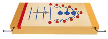
Using model calculations of surface wave scattering from hard spheres, we consider here focussing arrangements built from scattering centers (see Fig. 1), designed to achieve ultra-narrow peak widths. Complex interference patterns are obtained and analyzed for parabolic and semi-elliptic geometries. It is shown that in this way locally enhanced electron densities with sub-Å lateral size can be realized.
The guiding idea for our approach is to design quantum mechanical (electronic) states with effective widths and in real space and in momentum space, respectively, such that forms a spike of width . Heisenberg’s uncertainty relation requires that , where is Planck’s constant. While this fundamental principle of quantum mechanics inevitably controls any measurement process, it is important that the uncertainty relation does not preclude the possibility to structure the electronic wavefunction on a lengthscale much smaller than . Therefore, the principles of quantum mechanics do not set a lower limit for generating ultrasmall electronic structures, although these will possibly have a small local probability density in the spike volume . Rather, in a superposition of quantum mechanical waves, is often limited by the largest available momentum, which thereby imposes an upper limit on . For the purpose of focussing electronic waves in a crystalline solid this suggests to use high-energy waves preferentially in band states with a large effective mass.
To explore the size of the smallest area into which the electrons can be focussed with practical experimental setups, we performed model calculations in two space dimensions. Scattering centers of radius are arranged in open focussing geometries with either parabolic or semi-elliptic shape (see Fig. 1). An electronic surface wave, generated for example by a tunnel junction, is considered to enter the focussing arrangement as a plane wave with wavevector . The wave propagates along the symmetry axis of a regular arrangement of hard disks, with which we model individual atoms placed on a metallic surface with a spacing as is typical for Fe adatom corrals Eigler ; Heller . For long wavelengths , realized for surface state electrons on copper (111) surfaces, only isotropic s-wave scattering is significant. In this case, multiple scattering events and absorption from the scattering centers can be straightforwardly considered Heller . For shorter wavelengths, the established scattering analysis has to be extended to include higher angular momentum scattering channels.
In the absence of multiple scattering the scattering state has the asymptotic form (for )
| (1) |
where denotes the position of the -th scattering center, and measures with the polar coordinates and the relative position to the disk at . Introducing partial wave phase shifts, the scattering amplitude follows as
| (2) |
The parameter counts the scattering channel; the corresponding phase shifts are determined by , where and denote the Bessel functions of the first and second kind, respectively.
In the restriction to s-wave scattering, repeated scattering events are included by extending Eq. (1) to
| (3) | |||||
Here, for scattering centers with accounts for the phase factors related to the individual disk positions. The amplitudes for the waves scattered from the disk at to the disk at () form an matrix with
| (4) |
where . Similarly, the amplitude of the wave scattered from to is
| (5) |
The scattering amplitude is related to the s-wave phase shift by
| (6) |
The possible partial absorption of the incident electronic surface wave by inelastic scattering and scattering into bulk states is incorporated by allowing the phase shifts to become complex Heller , corresponding to the replacement in Eq. (6). Henceforth, is a real number; the absorption coefficient is 1 for non-absorbing adatoms and vanishes for complete attenuation.
For wavelengths which become almost comparable to the size of an atom, higher angular momentum scattering channels are important. To give an example, for (see below) the scattering phase shifts in s-, p-, and d-channels are , , and . With the restriction to double scattering from each disk the ansatz for the asymptotic scattering state is extended to
where is the angle for the position of the scattering disk in the polar coordinate system attached to disk . Without absorption, and neglecting the still small contribution of the d-wave scattering channel only, the s- and p-wave contributions ( and ) are included in the angular dependent scattering amplitude given in Eq. (2).
In a first attempt, the focussing properties of a device consisting of two parabolic “quantum mirrors” arranged like a reflector telescope, have been calculated. The substrate was assumed to be the Cu (111) surface, and 29 hard disks with radius Å were chosen to present Co3+ ions as scatterers. The focal distance of the parabola is Å, and the average disk spacing is 8 Å. The wavelength of the incoming wave was taken to be Å. At this wavelength , so that only s-wave scattering has to be considered. In Fig. 2 we show the resulting absolute square of the scattering state. Guided by the successful quantitative analysis of the current-voltage characteristics at the center of a circular quantum corral of iron atoms on a copper surface Heller , the “black dot” attenuation limit was adopted. The image shown in Fig. 2 is the pattern that would be observed in a standard STM local density of states measurement.
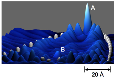
Near the tip of the parabola intense interference peaks with a full width at half maximum (FWHM) Å are produced (see for example peak A in Fig. 2). Due to the decay of the amplitude for the scattered waves the peak heights are larger the closer the peaks are to the scattering atom comment . Resulting from the focussing of the second, smaller “quantum mirror” additional peaks emerge near its focal point (see for example peak B in Fig. 2). The width of peak B, Å at FWHM, is just fractions of the incoming wavelength. The peak, however, has a small intensity.
There are obvious routes to further improve the focussing. First, materials capable of sustaining surface waves with considerably smaller wavelengths may be used. The goal to achieve interference peaks with subatomic widths precludes the use of surface eigenstates of noble metal surfaces, whose typical wavelengths are Å Davison . The recently observed Friedel oscillations on beryllium (0001) surfaces with wavelengths as short as 3.2 ÅBe suggest Be as a candidate material. Other options for tuning the electronic density distribution include using non-monochromatic waves and optimizing the arrangement of the surface adatom scatterers and the geometry of the quantum mirror. The development of a mathematical algorithm to select a focussing arrangement is quite a non-trivial task, and we have therefore explicitly tried several device geometries. Of the ones explored, particularly sharp peaks were obtained by using a semi-ellipse, as we will demonstrate in the following.
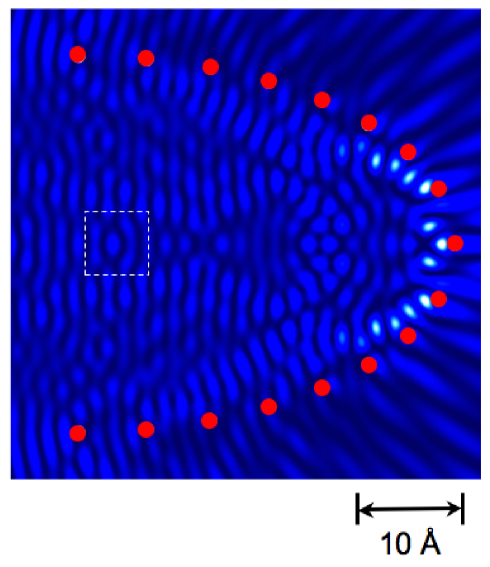
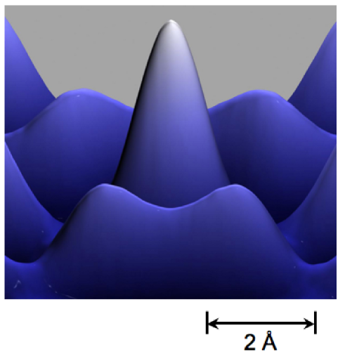
As shown in Fig. 3, 17 hard disks were placed on the contourline of a semi-ellipse with eccentricity and an average disk spacing of 6 Å. In this calculation the wavelength of the incoming wave of 3.2 Å and a disk radius of again Å was chosen. Fig. 3 shows the resulting contour plot of for the scattering state calculated from Eq. (Focussing Quantum States). The complex structures in this interference pattern originate in part from the angular dependent p-wave scattering channels, which have no counterpart in classical geometrical optics. Fig. 4 shows a larger magnification of the area marked by the white dashed square in Fig. 3. This area contains the most prominent constructive interference peak in this semi-elliptic focussing quantum mirror geometry. The peak has an anisotropic shape with an almost elliptic cross section; along the horizontal direction the FWHM of this peak is merely 0.92 Å. This is less than 2 Bohr radii. The peak width is therefore smaller than the nominal size of the 1s orbital of hydrogen.
So far we have not made an attempt to uniquely determine the optimum disk arrangement, which leads to the sharpest interference structure. Alternative focussing geometries with different selected positions of the scattering centers may very well lead to even sharper interference peaks. Initial ideas of “wave function engineering” by a special-purpose design of quantum corral geometries have recently been formulated in the attempt to generate special predefined mirage phenomena Correa . It is likely that similar strategies can be followed to identify arrangements of scattering centers with optimized focussing properties. If surface waves with wavelengths of just a few Å are considered, such optimization strategies will necessarily have to include also non–-wave scattering channels.
Our calculations reveal in a proof-of-principle that special arrangements of individual atoms on surfaces allow to create electron states with diameters comparable to the size of a hydrogen atom. These states may be coupled to bulk states and be used in devices such as highly focussed sources of tunneling electrons, as for example required for STM tips. The focussing of spin polarized surface states may furthermore allow to image magnetic structures on the atomic or subatomic scale. The controlled design and device applications of electronic structures on the sub-Å scale may therefore emerge as a real possibility.
We thank F. Giessibl, D. Vollhardt, G. Schön, Ø. Fischer, M. Sekania, C. W. Schneider, T. Kopp, R. Claessen, and D. Pohl for thoughtful discussions. This work was supported by the BMBF (EKM-project 13N6918) and the Deutsche Forschungsgemeinschaft (SFB 484).
References
- (1) M. F. Crommie, C. P. Lutz, and D. M. Eigler, Nature (London) 363, 524 (1993); Science 262, 218 (1993).
- (2) See the IBM homepage at http://www.almaden.ibm. com/vis/stm/hexagone.html.
- (3) Y. Hasegawa and P. Avouris, Phys. Rev. Lett. 71, 1071 (1993).
- (4) L. Bürgi, O. Jeandupeux, H. Brune, and K. Kern, Phys. Rev. Lett. 82, 4516 (1999).
- (5) E. J. Heller, M. F. Crommie, C. P. Lutz, and D. M. Eigler, Nature (London) 369, 464 (1994).
- (6) J. Kliewer, R. Berndt, E. V. Chulkov, V. M. Silkin, P. M. Echenique, and S. Crampin, Science 288, 1899 (2000).
- (7) H. C. Manoharan, C. P. Lutz, and D. M. Eigler, Nature (London) 403, 512 (2000).
- (8) The theoretical work on quantum corrals and mirages was recently reviewed by G. A. Fiete and E. J. Heller, Rev. Mod. Phys. 75, 933 (2003).
- (9) See also A. A. Aligia and A. M. Lobos, J. Phys. Cond. Mat. 17, S1095 (2005) and references therein.
- (10) P. T. Sprunger, L. Petersen, E. W. Plummer, E. Lægsgaard, and F. Besenbacher, Surface Science 275, 1765 (1997).
- (11) W. Heisenberg, Z. Phys. 43, 172 (1927).
- (12) S. G. Davison and M. Steslicka, Basic Theory of Surface States (Oxford, New York, 1996)
- (13) Because we use the asymptotic form for the scattered waves, which is only very accurate on distances larger than 5 atomic radii, the amplitude for is overestimated in the very near vicinity of each scattering disk.
- (14) A. A. Correa, F. A. Reboredo, and C. A. Balseiro, Phys. Rev. B 71, 035418 (2005).