Self-assembled nanowires on semiconductor surfaces
Abstract
A number of different families of nanowires which self-assemble on semiconductor surfaces have been identified in recent years. They are particularly interesting from the standpoint of nanoelectronics, which seeks non-lithographic ways of creating interconnects at the nanometre scale (though possibly for carrying signal rather than current), as well as from the standpoint of traditional materials science and surface science. We survey these families and consider their physical and electronic structure, as well as their formation and reactivity. Particular attention is paid to rare earth nanowires and the Bi nanoline, both of which self-assemble on Si(001).
1 Introduction
As the scale of architectures in integrated circuit design continues to be reduced, the dimensions of present-day interconnects are on the scale of tens of nanometers, and the interconnects for next-generation nanoelectronic devices may well be just a few nanometers in lateral dimension. Furthermore, the incorporation of nanometer-scale components, such as active molecules, into integrated circuits will require interconnects of a similar scale. On these scales, self-assembled nanowire systems are becoming increasingly interestingBowler2004 ; Barth2005 , as conventional lithographic techniques reach their limits around 10-15 nmChen1993 and SPM-based nanolithographyHashizume1996 methods lack scalability. Moreover, the introduction of such “bottom-up” technology, based on naturally nanometer-scale components to complement or even replace the current “top-down” technology is likely to require completely different architectures. One example is the “crossbar” architectureHeath1998 , in which active molecules are used as devices at the junctions between two perpendicular nanowires. This architecture is designed to take advantage of the typical product of self-assembly schemes – an array of parallel wires – rather than relying on controlled positioning of individual wires. Over the last ten to fifteen years, a number of systems have been identified which yield self-assembled nanowires on semiconductor surfaces, and stem from a mixture of serendipity and deliberate design. There are only a few systems which provide long, straight nanolines on flat terraces. In/Si(111)Nogami1987 (amongst other metals) and Pt/Ge(001)Gurlu2003 are examples of systems which undergo surface reconstructions leading to 1D atomic chains with metallic properties. On the Si(001) surface, the Bi nanolinesNaitoh1997 ; Miki1999a appear to be the only example of an atomically-perfect, straight, self-assembled 1D nanostructure, but are not metallic. Aside from fortuitous discoveries, symmetry-breaking by use of a vicinal surface to produce and array of steps can be used to grow long, straight nanowires of many metals, including Au, Bi et al.Baski2001 , and 1-D nanoscale structures can be designed by taking advantage of anisotropy in the heteroepitaxial strain between the Si(001) surface and an appropriate deposited material. The rare-earth silicides are the archetype of this methodPreinesberger1998 . Within the family of rare-earths (as well as scandium and yttrium), a close lattice match can be obtained in one direction, with a variety of positive and negative lattice mismatchs in the orthogonal direction. By choosing the right material, metastable 1D nanoscale structures 3-10 nm wide and hundreds of nanometres long can be formed. These have some phenomenological similarities with the Bi nanolines, as will be described. This review will survey the growing field of nanowires on semiconductor surfaces, with the focus on the Bi/Si(001) nanoline system, whose importance is explained in the next section.
The study of semiconductor surfaces has been revolutionised over the last twenty years by the advent of two techniques which give real-space atomic scale information: Scanning Tunneling Microscopy (STM) and electronic structure modelling (in particular, Density Functional Theory, or DFT). The two techniques are complementary, in that STM gives an approximate answer to an exact question (i.e. the structure of the real Si(001) surface), while DFT gives an exact answer to an approximate problem (i.e. the lowest-energy structure of a computation cell containing a few Si dimers, and a few layers of bulk-like Si). While these techniques between them enabled the clear identification of the Si(001) reconstruction, even today there is some controversy about the exact nature of the buckling of dimers on Si(001) at low temperaturesSagisaka2003 . In the same way, the understanding of the structure and properties of the nanolines surveyed in this paper has been greatly enhanced by a close collaboration between experiment and theory. The benefits of this synergistic approach will be drawn out throughout the discussion.
1.1 Introducing the Bi nanolines
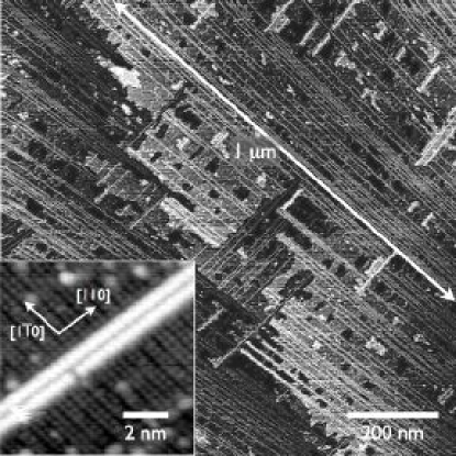
The Bi:Si(001) nanoline system, which will be the focus of this review, was discovered about ten years ago. As can be seen from the examples in Fig. 1, they grow perfectly straight along the directions on the Si(001) surface for hundreds of nanometres, apparently limited only by the terrace size of the underlying substrate. When they encounter a step edge, they will either grow out over lower terraces in a long, narrow promontory, or they will burrow into higher terraces, until a deep inlet is formed. They have a constant width, 1.5 nm or four substrate dimers, and are very stable. So long as the temperature is not so high that the Bi can evaporate, they are stable against prolonged annealing, maintaining the same width. This is quite unlike the rare earth silicide systems which in most cases (Yttrium being the probable exception) will coarsen into 3D epitaxial islands with long anneals. There are no other elements which produce perfect nanolines on the Si(001) surface, although there is some evidence to suggest that Sb nanowires with the same appearance as the Bi nanoline form in the presence of surface hydrogenKubo1999 , and DFT modelling that indicates that a Sb nanoline would be stableWang2003 . There has also been a suggestion that Er may form nanolines of the same structureWang2005 (as opposed to silicide wires), but this remains unconfirmed.
Structurally, the Bi nanoline is unique amongst nanoline systems—it is neither a periodic reconstruction of the surface, nor the result of anisotropically strained heteroepitaxial growth of one bulk structure on another. In fact, it is somewhere in between. The nanoline structure is built around a pair of Bi ad-dimers, on top of a complex subsurface reconstruction which is responsible for many of the nanoline’s remarkable properties, such as the extreme straightness; this will be explained in detail below. In this article, we intend to describe the formation, structure and properties of this system, setting it in the context of other nanoline systems, particularly the rare-earth silicide family.
1.2 Overview
The paper is laid out as follows: in Section 2 we consider the methods used to examine the systems, both experimental and theoretical; in Section 3 self-assembled nanowire systems other than the Bi:Si(001) nanowire system are described, with particular reference to the rare-earth silicide family; in Section 4 the Bi:Si(001) nanowire system is examined in detail, and in Section 5 the state of the field is considered and conclusions are drawn. In considering the nanowires in Sections 3 and 4 we consider first the formation and structure of the systems (including the effects of annealing), followed by the electronic properties (including conductance data where available) and finish with the reactivity of the systems.
2 Methods
2.1 Hot STM
Since its invention in 1982 by Binnig and Rohrer at IBM, STM has allowed researchers to image dynamic surface processes, in real-space, with near-atomic resolution. STM as a technique bridges a variety of disciplines. In surface physics, STM is unique as a real-space probe of electronic density of states of individual species; the STM tip can be a passive observer of surface chemical reactions, and also an active catalyst of these reactions; and STM allows for the direct observation of many phase transformation processes, albeit in 2D rather than 3D. However, this is not meant to be a review of capabilities of STM; for that, the reader is pointed to classic books on the subjectJChen1993 ; Wiesendanger1994 . Here a few comments are made, which are pertinent to the particular challenges of elevated-temperature (‘hot’) STM for the study of epitaxial growth.
Surface reactions can be followed at room temperature by using quench experiments, in which a high-temperature surface is cooled rapidly to freeze in a snapshot of an evolving surface, for example in the growth of III-V semiconductor surfacesAvery1997 . However, the quenching process may introduce spurious surface features, and so it is preferable to image the surface in-situ, i.e. at temperature. The ability to vary the sample temperature makes it possible to image a surface in the process of changing, rather than after it has changed. To give just one example, the phase transition between the (11) reconstruction and the (77) reconstruction on the Si(111) surface, at around 1100K, has been observed directly in both directions, by careful control of the temperature across the transitionMiki1992 . For useful observations of dynamic processes, the speed of the reaction must be matched to the rather slow imaging rate of an STM. One example is the motion of step edgesSwartzentruber1996 . At around 300∘C, step motion can be imaged as the addition or subtraction of 4 atoms between STM images. However, above about 500∘C, the step edge will have moved significantly in the time taken for the STM to scan one line. Thus from line to line, the step will be in different places, as it oscillates about a mean position. In STM, therefore, fast-moving steps have a streaky appearance above 500∘C, as may be seen in Fig. 19. Furthermore, mobile species may be invisible at elevated temperatures, either due to the decrease in contrast, or due to their mobility.
Surface chemical processes, such as the diffusion of Si atoms on Si(001)Swartzentruber1996 or the decomposition of a moleculeRezaei1999 , can be studied at the single-species level, and complete chemical reaction pathways from initial adsorption can be followed through to complete decompositionWang1994 ; Owen1997b . Kinetic information such as activation barriers can be extracted, and any metastable intermediate structures can be imaged, giving a unique insight into the reaction process. The ability to control the substrate temperature is particularly important in studies of epitaxial growth, where the kinetic pathways available at different temperatures will determine the surface morphology. In the case of Si/Si(001) and Ge/Si(001) epitaxy, it has been possible to image the surface simultaneously with the deposition of material, and therefore observe directly the nucleation of islands, and the growth of these nuclei into 1D, 2D and 3D islands, along with associated processes, such as the ripening of epitaxial islands, surface stress relief mechanisms, and the transition from island growth to step flow growth modesVoigtlander1997 ; Owen1997c ; Goldfarb1997b , all of which processes occur at different sample temperatures.
However, these added abilities bring with them a penalty in sensitivity. There is generally a loss of resolution due to thermal noise above room temperature, and a loss of stability, with thermal drift making it hard to image the same area for extended periods. In many of the high-temperature STM images shown here, the nanolines have a curved appearance. They have no curvature themselves, the appearance comes from the drift during scanning. Furthermore, imaging of epitaxial growth necessarily involves imaging a surface where there are many atoms loosely bound to the surface, or in the gas phase being deposited. In this situation, it is very easy for atoms to stick to the STM tip, which can have adverse effects on the imaging, and it is usually preferable to obtain stable imaging conditions rather than achieve the highest possible resolution, which is generally a more unstable situation. For the same reason, Scanning Tunneling Spectroscopy (STS), or Current Imaging Tunneling Spectroscopy(CITS)111A process in which a rapid voltage ramp is applied to the STM tip while in a fixed position above the surface, generating an I/V curve from which the LDOS can be measured, becomes unfeasible at elevated temperatures. It is generally better to take a series of images of the same area at different bias voltages, giving voltage contrast of an object, although as the feedback loop is active in this situation, the tip-sample distance will vary, and so the information gained is not equivalent to STS/CITS. Thus these limitations mean that while high-temperature STM brings the unique ability to study evolving surface morphology in real-space, it is not always the best way to study growth surfaces. A combination of high-temperature studies, and room-temperature studies of quenched surfaces, is likely to provide a fuller description of a system.
2.2 Electronic Structure Modelling
There have been a number of books on modelling techniques published recentlyMartin2004 ; Finnis2004 , so this section will feature only a brief description of the techniques used for modelling of semiconductor surfaces, concentrating on electronic structure calculations (both semi-empirical and ab initio). These techniques retain the quantum mechanics of the electrons while treating the ions classically.
The first problem to consider is how to model a semi-infinite piece of material (that is, a surface). The approximation that is used is to consider a small piece of appropriate material with boundary conditions. Generally, one of two solutions is used: either a cluster of atoms, with the dangling bonds on the edges terminated in some suitable way (e.g. hydrogen), or a slab of atoms with periodic boundary conditions in two or three directions. A cluster allows a smaller number of atoms to be used than a slab, but has the drawback that it is hard to allow for long-range strain effects (such as those caused by reconstructions or steps on surfaces). A slab approach requires care: the vacuum gap between repeating images must be large enough to prevent interactions, and the slab itself must be sufficiently thick to allow strain relaxation. The slab approach is more commonly used, particularly with the methods described below.
Once the system to be modelled has been defined, the calculation technique must be chosen. Putting aside quantum chemical methods for the sake of brevity (they scale rather poorly with system size—for more details, the reader is directed to one of many excellent books on the subjectSzabo1989 ), we will consider the semi-empirical tight binding (TB) technique, and the ab initio density functional theory (DFT) technique.
TBGoringe1997 ; Ordejon1998 postulates a basis set of atom-centred orbitals222For the class of methods known as ab initio tight bindingSankey1989 ; Horsfield2000 , the basis is explicit. for the wavefunctions; the Schrödinger equation can then be rewritten as a matrix equation, with elements of the Hamiltonian matrix formed from integrals between orbitals on different atoms. These Hamiltonian matrix elements are fitted to either ab initio calculated data or experimental results. For simplicity, the basis is often assumed to be nearest neighbour only (with a cutoff defined on the range of interactions) and orthogonal. Once the Hamiltonian has been defined, the band energy of the system can be found by diagonalisation of the Hamiltonian or other methods. The other energetic terms (e.g. Hartree correction, exchange and ion-ion interactions) are represented by a repulsive potential (often a pair potential).
Despite its apparent simplicity, TB is extremely effective, and generally qualitatively accurate, if not approaching quantitative. It has been shownSutton1988 that this TB formalism can be derived from DFT via a set of well-defined approximations, which explains to some extent its success. It is well-suited for a rapid exploration of configuration space (e.g. possible structures for some new surface featureBowler2002 ) provided that a suitable parameterisation exists for the bonds between different species. The fitting of parameterisations is non-trivial, and the transferrability of a given parameterisation (i.e. its accuracy in environments far from those in which the fitting was performed) is never guaranteed. Generally the matrix elements themselves are fitted to a band structure (or energy levels of a molecule), while their scaling with distance is fitted to elastic constants or normal modes of the system. TB retains quantum mechanics (since the energy is obtained by solving the Schödinger equation) while approximating the most complex problems.
DFTHohenberg-kohn-1964 ; Kohn-sham-1965 starts with an exact reformulation of the quantum mechanics of a system of interacting electrons in an external potential: the result is a set of equations for non-interacting electrons moving in an effective potential with all the complex electron-electron interactions in a single term, known as the exchange-correlation functional (it is a function of the charge density, which is itself a function of position, hence “functional”). Unfortunately, the form of this functional is not known, and must be approximated, for instance with the local density approximation (LDA) or one of the generalised gradient approximations (GGA).
DFT has been extremely successful in many areas of physics, chemistry, materials and, increasingly, biochemistry, particularly when combined with the pseudopotential approximation. The hard nuclear potential and the core electrons of each atom are replaced with a single “pseudopotential”, and only the valence electrons are considered, leading to a softer potential. This approximation is most effective for atoms where there is considerable screening of the valence electrons by the core electrons (e.g. in Si the 3s electrons are screened by the 1s and 2s shells, while the 3p electrons are screened by the 2p shell); in first row elements and first row transition metals, this is a much smaller effect, leading to the development of “ultrasoft” pseudopotentials. These issues are discussed in more detail in many excellent books and reviewsLindan2002 ; Martin2004 . The essential point to note is that DFT is widely used for electronic structure calculations, and provides results which are accurate to within approximately 0.1 eV.
An important development in electronic structure techniques over the last ten years is that of linear scaling techniquesGoedecker-1999 . Standard techniques for solving for the ground state, whether TB or DFT, scale with the cube of the number of atoms in the system (either because matrix diagonalisation scales with the cube of the matrix size, or because the eigenfunctions spread over the whole simulation cell, leading to cubic scaling when they are orthonormalised). This scaling places rather strong restrictions on the sizes of system which can be modelled, even on massively parallel machines: for ab initio methods, going beyond 1,000 atoms rapidly becomes prohibitive, though somewhat larger systems can be addressed. However, since electronic structure is fundamentally local (consider bonding as an example), the amount of information in the system should be proportional to the number of atoms in the system. Tight binding methods which take advantage of this (e.g. refs.Li1993 ; Goedecker1994 ) have been widely used for some time, allowing calculations on many thousands of atoms. The implementation of linear scaling DFT algorithms has proved significantly harder, though recent efforts in nearly linearfattebert00 and linear scaling methodsOzaki2001 ; soler02 ; Bowler2002b ; Skylaris05 suggest that these techniques are starting to produce useful and general results.
2.3 Modelling STM
One of the challenges of using STM to examine semiconductor surfaces is that the current arises from both geometric and electronic structure, though this is less true at high biases (where height or geometric structure will dominate). Some technique is required to understand these changes, and to test proposed structures against experiment. The field of STM simulation is a complex one (in part because the structure and composition of the tip is unknown); the interested reader is referred to excellent reviews for further informationBriggs1999 ; Hofer2003 . We will briefly summarise the simplest and most common approximation used, and discuss how the experimental-theoretical interaction can best proceed.
The most commonly used approach is the Tersoff-Hamann approximationTersoff1985 . This asserts (via a careful series of approximations) that the tunneling current is proportional to the local density of states (LDOS) due to the sample at the position of the tip. In effect, the tip is assumed to have a flat density of states. This approach is directly equivalent to considering the projected charge density (i.e. the partial charge density due to each band for bands within of the Fermi level). It is qualitatively accurate, though will not reproduce the observed corrugation values correctlyHofer2003 .
The authors are of the opinion that for true success in investigating nanowires (and other systems) on semiconductor surfaces, a close collaboration between experiment and modelling is required. Any successful collaboration depends on a number of factors, but the key factors, we believe, are frequent, easy correspondence, an understanding of the limitations and abilities of the appropriate techniques, and trust between the different sides in the collaboration. The last point extends to sharing of unpublished data, and extensive discussion of possible courses of action. The three authors have been working together in different combinations for ten years (leading to around 20 joint publications), and we find that our collaboration is still immensely fruitful.
3 Other Nanowires
While the Bi/Si(001) nanolines have remarkable structural qualities, they are not the only self-assembled nanowire system on semiconductor surfaces. In this section we present an overview of these other nanowire systems (more details are presented elsewhereBowler2004 ), and we will consider in more detail the most important of these systems, the rare-earth silicide family, focussing on their structure and formation, electronic properties and reactivity.
A variety of metals have been found to self-assemble into nanowires or nanolines on the Si(001) surface, though none with the perfection of the Bi nanolines. The simplest way in which to form 1D structures on the Si(001) surface is by epitaxial growth. An island nucleus is essentially an ad-dimer, which sits between the dimer rows. The two pairs of Si dimers which support the ad-dimer are distorted by its presence, and so are attractive adsorption sites for further ad-atoms or ad-dimersSwartzentruber1997 . This process has been described as a surface polymerisation reactionBrocks1993 . The long sides of the string, which are equivalent to A-type steps on this surface, have a very low sticking coefficient which keeps the island from broadening at lower growth temperatures. Deposition of Group III and Group IV elements on Si(001) will therefore result in long 1D chains of dimersEvans1999 ; Dong2001 ; Takeuchi2001 ; Srivastava2004 ; Albao2005 . However, there is little control over the length or structure of these wires, and they are unstable against annealing, eventually reorganising into compact islands. The Pt/Ge(001) systemGurlu2003 forms nanowires through a complex surface reconstruction, resulting in a system with a high degree of perfection, which approaches that of the Bi nanolines. When annealed to high temperatures, arrays of atomically perfect nanowires of Pt/Ge form, each of which is 0.4 nm wide with a spacing of 1.6 nm between the wires.
Sideways growth of two-dimensional islands can also be blocked by introduction of missing dimer trenches. These form to relieve surface stress, either because of contamination by a small amount of a transition metal such as Ni, or through heteroepitaxial growth of another material such as Ge. The trenches tend to line up in a semiregular array, giving an approximate (2n) reconstruction in LEED, with n8-12 (though the regularity of the trenches is rather poor). This method has been used to deposit a variety of metals, such as FeKida1999 , GaWang2002 and InLi2001a (using the Ni-based technique) and the molecule styreneZhang2004 . The result is long-range, reasonably well ordered wires of the metals, though their properties have not been characterised.
The 2D symmetry of the surface can also be broken deliberately by the use of vicinal substrates to produce regular arrays of stepsLin1998 which can then be decorated with materials such as goldBaski2001 ; Losio2001 ; Lee2002 ; Ahn2003 ; Crain2003 and BiCho2004 . This approach is used primarily on Si(111), although with an extreme orientation towards (112) directions the surface might be labelled Si(557) or Si(5 5 12) depending on the angle. The resulting step reconstructions comprise chains which are metallic and one-dimensional; early observations suggested possible observations of Luttinger liquid behaviourSegovia1999 , though this has been disputedLosio2001 ; Ahn2003 . Their spacing can be controlled to some extent by varying the angle of miscut of the surface.
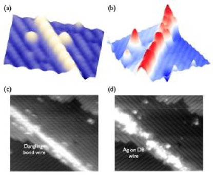
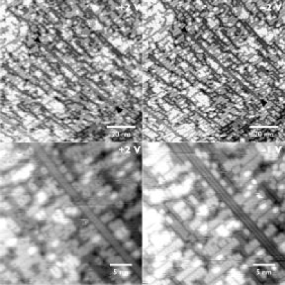
As an atomic-scale extension of the idea of lithography, the Si(001) surface has been passivated with atomic hydrogen (forming the monohydride phase) and individual hydrogen atoms removed with an STM tip to form atomic-scale patterns. The wire formed by removal of hydrogen atoms along (or across) a dimer row is known as a “dangling bond” wire (or DB wire)Shen1995 ; Watanabe1996 ; Watanabe1997 ; Hitosugi1997 ; Hitosugi1999 ; Bird2003a and is predicted to show conduction effects similar to conjugated polymers with polaronic and solitonic effectsBowler2001 ; Todorovic2002 ; Bird2003 . An example of a dangling-bond wire is shown in Fig. 2(a). These wires have been reacted with a variety of adsorbates including ironAdams1996 , galliumHashizume1996 ; Hashizume1997 , aluminiumShen1997 , silverSakurai2000 and organic molecules such as norbornadieneHersham2000 ; Abeln1998 ; Abeln1997 . However, although for a single row of dangling bonds, a perfect atomic wire can be formed, as with Ga in Fig. 2(b), for greater widths, as in Fig. 2(c,d), the dangling bond wire is more ragged, and the resulting wires (here Ag) are typically composed of a large density of small, roughly spherical crystals, which exhibit many imperfections and boundaries. A more elegant implementation stems from careful application of molecular chemistry to produce a directed reaction: when the monohydride surface was exposed to styrene and one hydrogen atom removed, self-directed growth of lines of styrene resulted from a chain reaction between each adsorbed molecule and an adjacent hydrogenLopinski2000 . Such self-organised methods are important for the growth of molecular nanowires on surfaces. However, for all these systems there is a lack of control over the size and length of the nanowires.
3.1 Structure and Formation of Rare-Earth Nanowires
A more promising materials system for nanowire growth on Si(001) is that of the rare-earth metal silicides. There has been extensive research on these systems because of their good conductivity and low Schottky barrier with siliconNetzer1995 , though this work concentrated on the Si(111) surface. Moreover, in the hexagonal phase some rare-earth silicides show a good lattice match with the Si(001) substrate in one direction, with a large mismatch in the other. Heteroepitaxial growth of these materials would therefore be expected to be constrained in the high mismatch direction, and facile in the other, resulting in long 1D islands. This is indeed what happens. The behaviour of the rare-earth nanowire systems on Si(001) has been investigated extensively, and nanowires have been observed under certain growth conditions. As the other major family of self-assembled nanowires on the Si(001) surface, we give a fuller description of this family for comparison to the Bi nanolines.
| Rare earth | a(Å) | (%) | c (Å) | (%) |
|---|---|---|---|---|
| ScSi1.7 | 3.66 | (-4.69) | 3.87 | (+0.78) |
| YSi2 (hexagonal) | 3.842 | (+0.05) | 4.144 | (+7.92) |
| Sm3Si5 (hexagonal) | 3.90 | (+1.64) | 4.21 | (+9.64) |
| GdSi2 (hexagonal) | 3.877 | (+0.96) | 4.172 | (+8.65) |
| DySi2 (hexagonal) | 3.831 | (-0.23) | 4.121 | (+7.32) |
| HoSi2 (hexagonal) | 3.816 | (-0.63) | 4.107 | (+6.95) |
| ErSi2-x (hexagonal) | 3.79 | (-1.30) | 4.09 | (+6.51) |
| YbSi2 | 3.784 | (-1.46) | 4.098 | (+6.71) |
The most common form of rare-earth nanowire (RENW) formed on Si(001) is thought to result from the anisotropic strain between the AlB2 crystal structure of the nanowire and the Si(001) substrate, leading to fast growth along the less-strained direction, and extremely limited growth along the more-strained direction. The mismatch for various silicides in the AlB2 hexagonal structure is given in Table 1. RENWs of this type have been reported for ErChen2000 ; Chen2002b ; Chen2002a ; Chen2002 ; Ragan2003 ; Fitting2003 ; Lee2005 ; Harako2005 , DyPreinesberger1998 ; Nogami2001 ; Preisenberger2002 ; Chen2002 ; Ragan2003 ; Liu2003b ; Liu2003a ; He2003 ; Liu2003 ; He2004b ; He2004a ; Lee2005 , GdChen2002 ; Liu2003b ; Liu2003a ; Lee2005 ; Harrison2005 and HoNogami2001 ; Ohbuchi2002 . For SmRagan2003 ; Lee2005 NWs only appear on vicinal substrates; other reportsNogami2001 ; Ohbuchi2005 find that on flat surfaces only rectangular, 3D islands are formed after a (23) layer). Bundles of NWs have been reported for YbKuzmin2004 ; again, early reportsNogami2001 ; Katkov2003 suggested that NWs were not formed, and 3D islands resulted from annealing. Though they are not rare-earth metals, similar NWs have been reported for both ScChen2002 and YLiu2003b ; Katkov2002 , resulting from the same combination of crystal structure and anisotropic strain. Although it forms a similar wetting layer on the substrate to Yb, Eu does not form NWsPerala2005 .
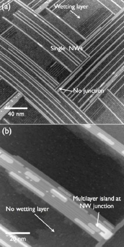
The resulting RENWs are found both individually and in bundles; the individual wires have sizes which vary from element to element but are in general 5-10 nm wide and less than 1 nm high. The wires grow extremely fast, reaching lengths of up to 1m; more interestingly they always run along directions and will grow out over step edges, drawing terraces with them, features that they share with Bi nanolines. The large-scale image in Fig. 3 is very similar to that of Bi nanolines at the same scale. For almost all materials, the surface of the wires shows a c(22) reconstructionChen2002b ; Chen2002a ; Ohbuchi2002 ; Liu2003a ; Liu2003 ; He2004a , though the Yb NWs, which are off-axis relative to the other RENWs, may have a (11) surfaceKuzmin2004a .
The Si(111) surface matches the lattice of the RE AlB2 structure reasonably well in all directions (with a mismatch of less than 2% for most metals)Netzer1995 and so would not be expected to give anisotropic growth, but GdSi2 NWs have been formed along step edges of a vicinal surfaceMcChesney2002 . These form because of a mismatch perpendicular to the step edge, and grow to over 1m long on appropriately prepared samples, with a width of 10 nm and height of 0.6 nm.
Other NW structures have been reported for transition metals on Si(111), for instance FeTanaka2005 (though these are rather short wires), NiLin2004 and TiStevens2003 ; He2003a . The growth mechanism for these wires is not entirely clear: the resulting NWs are 5 nm high and 5 nm wide (NiSi2), 10 nm high and 40 nm wide (TiSi2), though for both of these systems the NWs appear to grow into the substrate somewhat. There is a technique for growing NWs on Si(001), Si(110) and Si(111) explicitly relying on growth into the substrate, resulting in “endotaxial” NWs, which has been applied to DyHe2003 in the hexagonal AlB2 structure, as well as CoOkino2005 ; He2004b , which takes the CaF2 structure. The driving force appears to be kinetic in these systems: the long direction of the NW has an interface which grows faster than the short direction, though this is partly dependent on the structure of the interface below the surface.
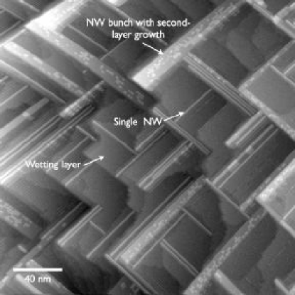
The growth and formation of the RENWs is not understood at an atomic level: they form extremely quickly (on experimental timescales) so that, for instance, hot STM cannot be used to observe formation of the lines. Unlike the Bi nanolines, which have a constant width, and do not change in width with annealing, the rare-earth nanoline family can take a variety of widths depending on the growth conditions. In the case of DySi2, single NWs of a consistent width form from the underlying (27) reconstructed wetting layer, as in Fig. 4. However, further annealing results in the formation of bunches of nanowires, which join together where they meet, and multilayer islands form. As strained coherent heteroepitaxial islands, the RENWs are only metastable; prolonged annealing will cause them to coarsen, and form large 3D islands. Overall, the deposition/anneal temperature must be in the window between 550∘C and 650∘C, and annealing time should not exceed 2-10 minutes. Below 550∘C or 2 minutes, the reaction will be incomplete and the NWs formed will be immature. Above 650∘C or 10 minutes the systems tend towards lower energy, thermodynamically stable states. In particular, Dy-Si(001) will form 3D islands if annealed for long times (e.g. 30 minutes for 0.86ML)Liu2003 with wires formed for shorter annealing periods. Annealing Er-Si(001) initially results in NWs, but as the annealing time is increased dislocations form in the NWsChen2002 . If the temperature is raised beyond 620∘C the same behaviour is seen, leading ultimately to coarsening into islandsChen2002b . A large-scale PEEM study of ErSi2Fitting2003 found that large NWs (which may have been bundles of nanowires—the technique does not have the resolution to distinguish) were not affected by annealing on a coarse scale. However, Gd shows more complex behaviour. Annealing studies of thin films of Gd found that both hexagonal and orthorhombic phases could formMolnar1998 , and that with longer annealing times the orthorhombic phase grew at the expense of the hexagonal phase. Long anneals of the Gd/Si(001) system, up to 620∘C for one hour, resulted in the formation of previously unknown silicide structures, which are aligned perpendicular to hexagonal silicide NWs on the same terraceHarrison2005b .
There are various useful observations of their behaviour which can be made:
-
•
A wetting layer with a characteristic reconstruction forms before the nanowires, and persists on the substrate with the nanowires; specific reconstructions have been observed for:
-
–
Eu-Si(001):(23)Perala2005 ,
-
–
Sm-Si(001):(23)Ohbuchi2005 ,
-
–
Yb-Si(001):(23)Kuzmin2003 ; Katkov2003 ; Kuzmin2004 ; Perala2005 and (24)Katkov2003 ; Kuzmin2004 ,
-
–
Nd-Si(001):(23) and (24)Katkov2003 ,
- –
-
–
Gd-Si(001):(24)Liu2003a , and (25) and (27)Liu2003a ; Harrison2005
-
–
Ho-Si(001):(24) and (27)Ohbuchi2002
-
–
-
•
The only system for which this does not happen is Er-Si(001)Chen2002b .
-
•
The system must be heated during deposition or annealed post-deposition to allow reaction of the rare-earth metal with the substrateChen2000 ; Nogami2001
-
•
Annealing the system for too long, or depositing at too high a temperature, can result in 3D islands rather than nanowires; this is discussed in more detail below.
As different metals have different properties for each of these categories, we will discuss them briefly in turn. Gd and DyLiu2003a form a (24) reconstruction first, followed by a (27) reconstructionLiu2003a ; Harrison2005 just prior to nanoline formation. Rather similar behaviour is seem for HoOhbuchi2002 . The metal fraction in the two reconstructions is 3/8 and 5/14 ML respectivelyLiu2001 ; Liu2003a . For these three metals, the presence of the wetting layer is intimately connected with formation and stability of the nanowires.
Despite the wealth of studies of ErSi2 nanowires, there are no reports of the structure and make-up of a wetting layer for this system; there is some evidenceChen2002b that once more than 0.05ML of Er is deposited, long chains of surface dimers form, followed by nanowires, with no intermediate reconstruction. Indeed, there are indicationsRagan2005 that the surrounding substrate is clean Si(001).
Another group of metals form closely related reconstructions: EuPerala2005 ; Kuzmin2005 , YbKatkov2003 ; Kuzmin2003 ; Kuzmin2004 ; Perala2005 , NdKatkov2003 and SmOhbuchi2005 all form (23) and in some cases (24) reconstructions; by contrast to Er, Dy, Gd and Ho, these metals are strained in both surface directions on contact with Si(001) (which might be expected to reduce the periodicity of any substrate wetting) and lack the main driving force seen before for nanowire formation. In general these metals do not form nanowiresNogami2001 ; Katkov2003 ; Kuzmin2003 though there are certain conditions where Yb can be made to form nanowiresKuzmin2004a of some kind, which may well be grown off-axis (in a different growth mode to the other silicide nanowires which grow with the c-axis aligned with the substrate).
It is also possible to induce nanowire formation in situations where they would not normally form, either because of uniform lattice matching (e.g on Si(111) surfaces, as mentioned above) or lattice mismatch in both surface directions using step edges. This technique has been successfully employed for Sm on Si(001)Ragan2003 ; Lee2005 and GdMcChesney2002 and DyHe2005 on Si(111).
3.2 Electronic Properties of Rare-Earth Nanowires
One of the original technological interests in rare-earth overlayers on Si(111) was the good crystal growth possible due to the interface between the silicon and the overlayer, and the conductivity properties. The films have good conductivity and a low Schottky barrier (0.4 eV on n-Si and 0.8 eV on p-SiNetzer1995 ).
Measurement of the conductivity of RENWs is a significant challenge. Full two-point or four-point measurements requires either a unique STM instrument (for instance one used to measure conductivity of CoSi2 nanowires on Si(110)Okino2005 ), or alternatively the formation of nanoscale contacts to a NWFujimori2004 . While significant progress has been made in this area recently, any measurements of conductivity will include the resistance of the interface between the NW and the contacts.
Scanning tunneling spectroscopy (STS) has been performed on various NWs: Dy and HoNogami2001 ; Ohbuchi2002 and GdLee2003 ; Lee2005 . While STS does not measure the conductivity along the NW, it does measure the local electronic structure, and in all cases the NWs are found to be metallic, while the surrounding reconstructed substrate is notNogami2001 ; Ohbuchi2002 ; Lee2005 . This is good evidence that the NWs are taking on the bulk silicide structure, which is conducting, and the wetting layer is an intermediate state which relieves strain.
Conductivity measurements of transition metal silicides on Si(111) and Si(110) have been madeLin2004 ; Okino2005 . These studies exemplify the two techniques for measuring NW conductivity: NiSi2 NWs were contacted by gold padsLin2004 , while four-probe STM measurements were made on CoSi2 NWsOkino2005 . These NWs are relatively large compared to the RENWs discussed so far: 15nm (Ni) and 60nm (Co) wide. The CoSi2 NWs showed a high Schottky barrier and conductivity equivalent to that of high quality thin films of CoSi2, while the NiSi2 NWs showed some signatures of quantum transport, though the conductivity of these wires was significantly lower than thin films; this is likely due to the overgrowth of the sample with SiO2 for transfer to the lithography apparatus.
3.3 Reactivity of Rare-Earth Nanowires
There is very little data on the chemical reactivity of the rare-earth nanowires. Thin films on Si(111) are susceptible to reaction with ONetzer1995 ; the RENWs oxidise rapidly in airRagan2005 , and transition metal NWs show signs of this (confirmed by the conductivity of NiSi2 NWs on Si(111)Lin2004 ). In the TM system, the NWs were overgrown with native oxide, and showed a significant decrease in conductivity relative to complete thin films of similar thickness, which is attributed to scattering at the NW surface/oxide interface.
Further information on the reactivity comes from the deposition of Pt on a surface containing ErSi2 NWs on Si(001)Ragan2005 . The Pt was deposited at room temperature and the sample was subsequently annealed. When STM images were taken they showed that the c(22) surface reconstruction on the NWs was no longer visible though the (21) substrate reconstruction was still present. Furthermore, the Pt-covered NWs were resistant to reactive ion etching and appeared stable when exposed to air for periods of up to 8 weeks; the Pt overlayer does appear to strain the NWs, however, leading to delamination of the NWs from the substrate if left untreated. Clearly there is much work to be done understanding the reactivity and stability of these NWs.
4 Bi Nanowires
The discovery that nanowires would form if a Bi-covered Si(001) surface was left to anneal around the Bi desorption temperature was made quite by chance. In 1995, in the Materials Department of Oxford University, two of the authors were investigating the surfactant-assisted growth of Ge/Si(001) using Bi as a surfactant, and were studying the properties of Bi/Si(001). When a sample which had been left to anneal at ca. 500∘C overnight was imaged, very large, flat terraces, and long, straight, bright lines (longer than the scanning range of the STM), running across the surface were found. These were the Bi nanolines. The first published image of the “nanobelts” was in 1997Naitoh1997 , and the first big study of their growth and properties came in 1999Miki1999a . In this section, we will discuss the atomic structure of the Bi nanoline, and its physical and electronic properties. We show that many of the properties stem from its unusual structure. The reaction of the Bi dimers with a variety of reagents, and the effect of burial of the nanoline will also be discussed.
4.1 Physical Structure
The physical structure is the key to understanding the properties of a nanoline system, and great effort has been devoted to identifying the structure of the Bi nanoline. In this case, the structure was identified by a synergy of STM observations with tightbinding and DFT simulations. The three different proposed models for the Bi nanoline are shown in Fig. 5. The two early models (shown as the top two models) share certain structural motifs. They contain a pair of Bi dimers set into the surface layer of the Si(001) crystal, whose compressive stress is relieved by missing dimer defects (DVs). The first model proposed, shown in Fig. 5(a), was based around a pair of Bi dimers in the surface layer, separated by a missing dimer defect, so as to relieve the local stress of the Bi dimersMiki1999a ; Miki1999b . This became known as the Miki model. The second proposed model, shown in Fig. 5(b), was based around a pair of Bi dimers with defects on either sideNaitoh2000 , which became known as the Naitoh model. However, the third model is more complex: a reconstruction of several layers of Si underneath the Bi dimers produces the nanoline core. This was named the Haiku modelOwen2002b 333It is named after the Japanese verse form, which comprises three lines of 5, 7, and 5 syllables, referring to the 5- and 7-membered rings of silicon in the reconstruction.. Of the three models, this structure is the only one to fit all the criteria which have been determined from STM observations, as well as having the lowest energy of the three. In this section, we will briefly review the historical process by which this structure was determined, and discuss the properties of the Haiku structure.
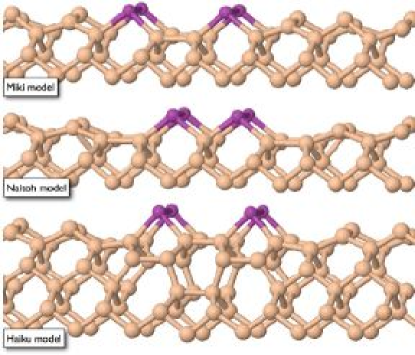
4.1.1 Early Models
Early STM images of the Bi nanoline were taken at elevated temperatureMiki1999a ; Miki1999b , in which the Si dimers were not resolved, and hence the registry of the nanoline with the substrate was unknown. This data suggested that the nanoline contained two features, which were probably Bi dimers, with a spacing of approximately 6.3Å, with a total width of about 1 nm, which was approximately equivalent to the space of three Si dimers. As the nanolines appeared bright at large bias voltages (in both positive and negative bias images) to dark at low voltages, it was also reasonable to assume that these Bi dimers were situated in the surface layer, rather than in an adlayer or in a subsurface layer. It was thought that Bi dimers embedded in the top surface layer would have considerable compressive stress, and on this basis, a model based around a 1DV, with Bi dimers to either side, was proposed. This was the Miki modelMiki1999a ; Miki1999b ; Bowler2000 . Tightbinding calculations of the Miki modelBowler2000 found that it was more stable than the (21) or (2n) Bi reconstructions, and that the formation energy of a defect in the line was high: around 1.1 eVBowler2000 (this number considers putting the Bi which has been removed as an ad-dimer on the surface; recent dataOwen2005b shows that the defect energy falls to 0.11 eV if the Bi dimer is placed in another Miki model; this point is discussed more fully in Section 4.1.3 below). DFT calculationsMiwa2002a ; Owen2002b ; Bowler2002 ; Miwa2002b agreed with those conclusions. The calculated LDOS showed that the Bi dimer states were further away from the Fermi level than those of the Si dimers and simulated STM images of the Miki structureMiwa2002a ; Miwa2002b ; Srivastava2004 showed that the line would appear dark at low bias voltages, in agreement with STM resultsOwen2003 ; MacLeod2005 . Testing by other methods appeared to confirm this structure. Photoemission spectroscopy experimentsOwen2002b found that the Bi 5d core-level spectra of the Bi nanowire was essentially identical to the spectra of the (2n) phase composed of Bi ad-dimers. This suggested that the local chemical state and registry of Bi adsorbates for both phases was the same, i.e. that the Bi was in the form of dimers in the top layer of the structure. X-ray photo-electron diffraction (XPD) experimentsShimomura2000 found a good fit between the experimental XPD data and simulated XPD intensity peaks from the Miki model. In particular, they confirmed the presence of Bi dimers parallel to the Si dimers and found the spacing between them to be 6.3Å, in agreement with the STM measurement, though it is important to note that the quoted distances are the result of a fit to the Miki model.
However, it was difficult to account for the extreme straightness of the nanoline with the Miki model, as the calculated kinking energy was very small, around 0.1 eV. A kinetic argument was put forward, which suggested that there was a stronger preference for incoming Bi dimers to line up at the end of the nanoline, and hence the nanoline would grow straightMiki1999a . Furthermore, the diffusion constant of a Bi surface dimer was high (this diffusion was required for a kink to form in a Miki model nanoline), and hence a line would remain straight once it had grown. Despite this explanation, the issue of the straightness of the Bi nanolines remained as a question mark over the Miki model.
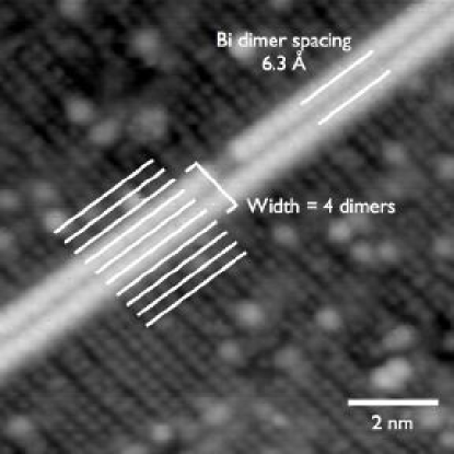
Subsequent room-temperature STM experimentsNaitoh2000 proved decisively that the Miki model could not be the structure of the Bi nanoline, as it had the wrong registry with the surface. Markers were placed on the surface of an image with the Si dimers resolved, as shown in Fig. 6, and by counting across the nanoline, the width was determined definitively to be four dimers, and not three as in the Miki model; moreover the Bi dimers lay between the Si dimers of the substrate, not in the same position. (This registry has been confirmed by every other STM measurement madeOwen2002a ; Owen2002b ; MacLeod2004a ; Wang2005 ; Miwa2005 ; Miwa2005b ; Owen2005b ). On the basis of the new STM data, the Naitoh model was proposedNaitoh2000 . Again this model was tested by atomistic calculations; a detailed study of the dimensions and simulated STM appearanceMiwa2002b ; Srivastava2004 ; Miwa2005b showed that again the nanoline would appear dark in STM at low bias voltages, but showed also that the spacing of the Bi dimers was too narrow, approximately 5Å, which could not be reconciled with the spacing of 6.3Å measured from STM. Moreover, the energy was considerably worse than the Miki modelOwen2002b ; Miwa2002b , and the kinking energy was still low. There was therefore no satisfactory structural model at this time.
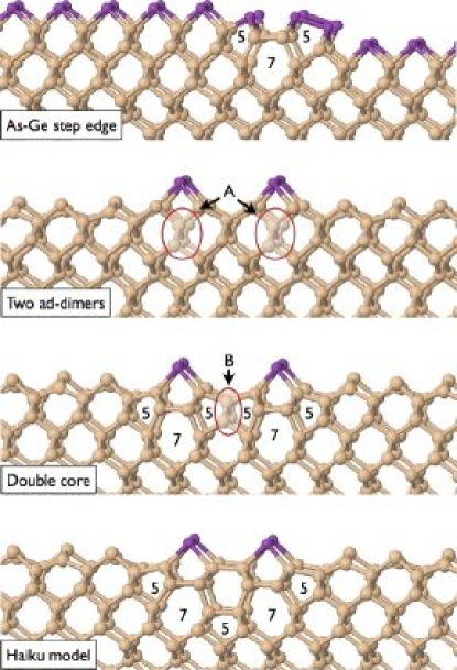
4.1.2 The Haiku model
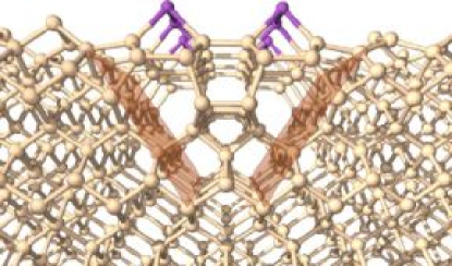
Inspiration for the structural model of the Bi nanoline arose from the structural model proposed for the B-type double-height step of As-terminated GeZhang2001 . At this step edge, bond rotation forms a pair of 5 and 7-membered rings of Ge, capped with As, shown in Fig. 7(a). While the Haiku structure appears to be a complex reconstruction, in fact the construction from a cell containing two Bi ad-dimers can be described schematically in two simple steps, as shown in Fig. 7(b)-(d). The first step is to rotate the second and third layer atoms underneath the Bi ad-dimers, so that the Si dimer atoms sink down into the surface. This creates the 5- and 7-membered rings also seen in the As/Ge step structure. The central four atoms are then removed, and the two halves of the structure bonded together, thus creating the Haiku structure. (N.B. This is not proposed as the formation mechanism, but is simply given as a means of understanding the substructure.) A linescan of the nanoline has been matched to the Haiku model, using the background Si dimers as reference marksOwen2002b . The positions of the Bi dimers match up extremely well to the peaks in the linescan, giving strong confirmation of this model. Other features of experimental linescans also agree well with simulated linescans for the Haiku modelOwen2005b ; Miwa2005 . DFT calculations of this new structureOwen2002b found that it was considerably more stable than the Miki model, which has been confirmed by subsequent modellingWang2003 ; MacLeod2005 ; Miwa2005 ; Miwa2005b . Although the Haiku structure shares several structural features with previous models—the top of the structure has two Bi dimers joined by rebonded second-layer Si atoms, as in the Miki model, while on the outside of the Bi dimers, there are more rebonded Si atoms, just as in the Naitoh model—the difference lies in the Si substructure; this mixture of 5 and 7-membered rings extends down many layers. Consideration of the core of the nanoline reveals that it is a small triangular section of hexagonal silicon, embedded in the diamond cubic silicon substrate, rather like the “endotaxial” RE nanowires mentioned in Section 3.1. The {111} planes that delineate the core are shown in red in Fig. 8. The hexagonal core of the nanoline does not exist as a bulk structure for silicon; it is particular to this nanoline structure. In this respect, the Bi nanoline is quite unlike the epitaxial rare-earth silicide family, which are essentially one bulk crystal grown epitaxially onto another bulk crystal, taking their shape from the highly anisotropic mismatch between the two. This core structure is responsible for many of the properties of the Bi nanoline. It will be difficult or impossible to kink, resulting in the extremely straight nanoline observed. As will be shown below in Section 4.2.4, the tensile strain field results in the repulsion of other nanolines, step edges and missing dimer defects. As a result, the nanolines will not grow sideways, will not grow together, and will not coarsen into larger islands, unlike the silicide wires. The electronic structure of the Haiku model has been studied in some detailOwen2003 ; Owen2004 ; MacLeod2005 ; Miwa2005b , and again the nanoline becomes dark in low-bias images — this effect is a property of the Bi dimers rather than that of the nanoline. Low-bias STM images reveal other electronic effects, which provide further confirmation of the Haiku structure, while ruling out the Miki structure. These features are discussed below in Section 4.3.
However, despite the wealth of agreement of the predictions from the Haiku model with experimental evidence, there has been no direct confirmation of the Haiku structure. The Bi nanolines are destroyed by exposure to air, while burial of the nanolines in a capping layer also changes their atomic structureSakata2005 ; Yagi2005 (though if done carefully the 1D character and dimerisation of the Bi can be preserved), so that cross-sectional TEM studiesMatsuhata2004 have not provided definitive confirmation of the core structure, and a recent X-ray Standing Wave(XSW) studySaito2003 which relied upon capping with amorphous silicon and whose results cast doubt on the Haiku model, cannot be regarded as a counterindication. The difficulties of burial of the Bi nanoline are discussed in Section 4.5. We note also that a recent suggestionMiwa2005b , that the height of the Bi dimers in the Haiku model is too far above the plane of the surface Si dimers based on XPDShimomura2000 , is not a significant piece of evidence against the Haiku model: the XPD data was fitted to the Miki model, thus naturally giving the wrong data for the Haiku. If a fit of the data to the Haiku model were to give height data which contradicted the atomistic modelling, then the model would have to be revisited.
4.1.3 Miki model revisited
Despite the apparent success of the Haiku model, the Miki model has continued to attract a large amount of attentionMiwa2002a ; Miwa2002b ; Srivastava2004 ; Miwa2005 ; Miwa2005b as a possible candidate for the nanoline structure. While in fact its incorrect registry with the Si substrate unambiguously rules it out as a candidate nanoline structureNaitoh2000 ; Owen2002b ; Owen2005b , it is an energetically favourable structure, and might be expected to be present on the Bi-covered Si(001) surface. With the benefit of hindsight, it can be seen that the Miki structure was indeed observed in early STM images of the Bi-rich surface. Fig. 9 shows that annealing a Bi-rich surface at 400∘C produces a large density of quite straight dimer vacancy (DV) trenches. In the filled-states image, Fig. 9(a), these appear to be composed of clean silicon. However. in the empty-states image, Fig. 9(b), there is contrast between the dimers adjacent to the missing dimer trenches and the rest of the surface. This contrast does not occur on the clean surface at this bias voltage, and so it can be inferred that the trenches are decorated by Bi dimers, i.e. the Miki structure has been formed. As with the Ge-induced DV trenches mentioned in Sec. 3, there is cooperative strain relief between a Bi dimer and a 1DV. Bi dimer/DV structures have the lowest energy/Bi dimer of any structures except the Bi nanolines. There is a kinking energy for these (2n) trenches of around 0.1eVOwen2005b . Hence the formation of a semi-regular array of Bi dimers reduces the energy further.
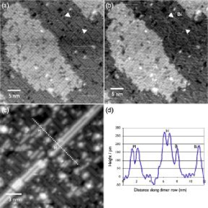
Further proof of the Bi decoration of 1DV trenches has been provided by a more recent experiment, in which a Bi-rich surface was quenched from 550 ∘C at an early stage of the annealing processOwen2005b . Here atomic hydrogen was adsorbed after cooling to enhance the contrast between Bi and Si significantly, as the H will adsorb easily to the Si dimers, but does not adsorb on BiNaitoh2000 ; Owen2002a ; Owen2005b , as can be seen in Fig. 6. It was found that the H termination increased the relative apparent height of Bi-related features by ca.150 pm, or 1.5Å. An example image is shown in Fig. 9(c). A linescan across both a Bi-decorated trench and a section of nanoline shows that the Bi-decorated trench is quite similar to the nanoline, but is lower and has a deeper depression between the two Bi dimers. STM linescans of the feature decorating DV trenches and the Bi nanolines Owen2005b compare very well to simulated scans of the Miki model and Haiku model respectivelyMiwa2005 , providing strong support for both these identifications. Furthermore, in this way, it has been shown that the Miki structure and the Bi nanoline co-exist, demonstrating once again that the Miki structure is not the nanoline, as has been recently suggestedMiwa2005b , but it is kinetically stable, even at high temperatures, due to the large activation barrier necessary to form the Haiku structure.
4.2 Formation and Properties of Bi nanolines
While rare-earth silicide wires have quite specific growth recipes in order that the nanowires do not coarsen, the Bi nanolines are robust to a wide variation in the growth conditions. The essence of Bi nanoline formation is that it is a competition between deposition and evaporation. A thick layer of Bi on Si(001) is only stable below the Bi bulk evaporation temperature (ca. 400∘C). Above this temperature, an epitaxial layer of 1-2 ML Bi is stable, and annealing of this surface will result in a surface with Bi nanolines co-existing with these Bi islands, as shown in Fig 10. The first-layer Bi forms a (2n) structure, with n=4 or 5Naitoh1997 ; Miki1999a ; Bowler2002 , and the second-layer Bi forms as small groups of dimers, which can be either parallel or perpendicular to the underlying Bi.
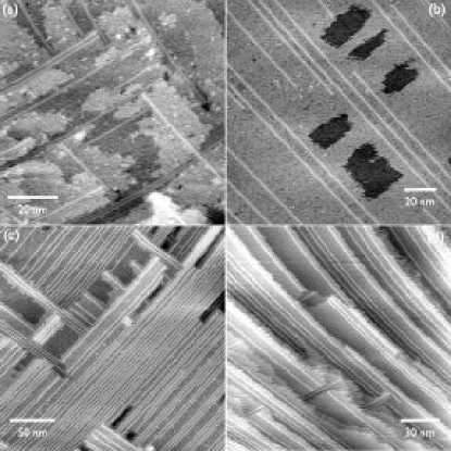
The threshold temperature at which Bi dimers on Si(001) will start to evaporate is around 500∘C, while the maximum temperature at which any Bi is stable on the Si(001) surface is around 600∘C. Deposition of Bi in this temperature window, or deposition of Bi at a lower temperature, followed by an anneal within this temperature window, will result in a surface comprising Bi nanolines on an otherwise clean surface, as in Fig. 11. However, the details of the growth recipe will determine the surface morphology at the end of the anneal, as is described below in Sec. 4.2.1. Of particular technological interest is the growth of majority-domain surfaces after long anneals. The Si(001) surface has two equivalent domains with the dimer rows running in orthogonal directions. On a typical Si(001) surface, these two domains will have roughly equivalent total areas. Single-domain surfaces form on vicinal wafers miscut along a direction, where the dimer rows tend to run perpendicular to the step edges. However, by long anneals of the Bi-rich surface towards the high end of the temperature window, majority-domain surfaces can be formed, even on flat surfaces. In this case, extremely long Bi nanolines grow, up to 1m, as can be seen in Fig. 12.
High-temperature STM observations of the annealing Bi-rich surface shows a consistent series of surface morphologies. Immediately after the end of Bi deposition, a relatively rough surface is obtained, with a high density of small islands, composed of a mixture of Bi and Si, as shown in Fig. 11(a). These will quickly disappear, but at the same time, nanolines begin to form, either on the terraces, or on one of the mixed islands. The nanolines grow out over the step edges in long, finger-like islands known as promontories, with a Bi nanoline surrounded by a thin strip of silicon. Examples of the growth of promontories are seen in Fig. 17, and more mature examples of this type of surface are shown in Figs. 11&12. The nanolines will not only form long, narrow promontories, but also the reverse, a deep inlet where a nanoline in one terrance has grown through an up-step into an upper terrace. The surface between the Bi nanolines contains a large density of mobile missing-dimer defects, apparent in STM as dark, fast-moving streaks. After further annealing, the missing dimer trenches begin to disappear, and the Bi nanolines remain on a very flat, featureless surface. Finally, the Bi nanolines themselves evaporate. In the following sections, we will give describe the surface processes which drive this sequence of events, and account for these observations. The interactions of the Bi nanoline and its associated strain field with defects and step edges in the terraces, and with each other, will be discussed and the possible nucleation mechanisms of this complex structure explored.
4.2.1 Growth Recipes
As shown above, annealing a Bi-rich surface at lower temperatures results in a surface containing a high density of missing dimer trenches, decorated with Bi dimers, i.e. the Miki structure. One feature of the Bi nanoline is the high temperature required to form it, implying a significant activation barrier to its nucleation. While the large number of growth parameters, such as flux, total amount deposited, substrate temperature, miscut angle and azimuth, provides a wide range of different possible recipes, as summarised in Fig. 13, there are essentially two routes to the growth of nanolinesMiki1999a . One growth method for the nanolines is to deposit a monolayer of Bi below this threshold temperature, and then anneal the sample until Bi nanolines form. After around 1 hour at around 500∘C, this will result in a surface with Bi nanolines and a background Bi-covered surfaceNaitoh1997 ; Miki1999a . Continued annealing of this surface will result in the desorption of the background Bi forming a surface similar to that shown in Fig.11(a), and eventually a surface similar to that shown in Fig. 11(b) is obtained. The second growth preparation route involves the deposition of Bi onto the surface within the desorption temperature window. Due to the lower surface coverage of Bi, and the higher temperature, a more ordered surface is obtained, and fewer, longer, Bi nanolines form. The final surface is much the same, however, corresponding to that shown in Fig.11(b). A high density of Bi nanolines can be built up by continuous Bi exposure for a long time, at a temperature in the upper half of the desorption window. In this regime, the nanolines are only stable for a few minutes in the absence of a Bi flux and small differences in stability, such as the ends of a nanoline, will be significant. Shorter nanolines, perpendicular to the prevailing direction, will tend to dissolve, so that a highly ordered surface with long, parallel nanolines is obtained, as in Fig.11(c). By use of a vicinal surface, the preference for one domain can be enhanced further, and a surface close to a single-domain surface can be obtained, as in Fig.11(d). A second method which produces a majority-domain surface, even on a surface without any intentional miscut, (the miscut angle is ) MacLeod2004a ; MacLeod2004b , produces a surface as shown in Fig. 12. In this case, a substrate temperature around 530∘C was used, 4.5 ML of Bi were deposited, with an anneal for around 40 mins. Comparison of Fig.11(d) and Fig. 12 reveals that in the former case, the nanolines are parallel to the prevailing step edges, while in the latter, they are perpendicular. Despite the large difference in morphology, the only differences between this recipe and that which produced Fig.11(c,d) are that continuous deposition for an extended period was not used, and the heating current used was AC, a strategy which was designed to reduce electromigration. Whether this is is the cause of the majority-domain surface remains unclear, but such large-scale single-domain surfaces are ideal for nanoelectronics applications.

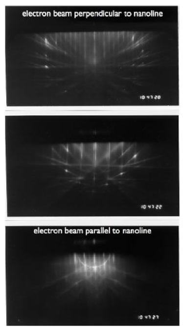
While STM can observe only a relatively small part of the surface, the large-scale order of the surface can be determined using electron diffraction methods such as RHEED. A series of RHEED patterns at different azimuthal angles of a single-domain Bi nanoline surface are shown in Fig. 14. Perpendicular to the nanolines, the RHEED pattern comprises vertical lines, while parallel to the nanolines, a ring feature is seen. The strength of these features demonstrates the long-range order generated by the nanolines, and means that their growth and development can be followed in real-time.
4.2.2 The Bi reservoir
In contrast to the silicide nanowires, which form very rapidly at the growth temperature and are only stable for about 10 mins. at that temperature, there is a significant incubation period before the nucleation of the Bi nanolines, and they will continue to grow for upwards of an hour after the deposition of Bi has finished. Thus the Bi required to generate the nanolines must come from a reservoir of Bi which is present on the surface. Where is this Bi located, and how does it affect the growth of the nanolines?
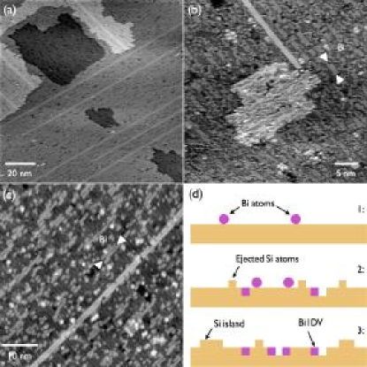
In images of the surface taken soon after the end of the Bi deposition, for example, Fig.11(a), there is often a high density of small islands on the surface. These islands have the same appearance as the rest of the surface; they are not islands of Bi dimers, as may be seen after deposition at lower temperatures, but appear to be mixtures of Si and Bi atoms. In general, such small islands are not stable at these temperatures, as has been seen in hot STM studies of Si homoepitaxy on Si(001)Voigtlander1997 ; Owen1997c . During growth, these small islands are stabilised by the high flux of Si atoms, but if the flux is cut off, a process similar to Ostwald Ripening occurs, in which these islands will decompose, and the material in them will move to step edges (which may be regarded as a very large island). The similarity of the behaviour observed here suggests that these islands are sustained by a flux of Si and Bi, which is produced during Bi deposition. For low coverages of Bi, the lowest-energy sites for Bi dimers which have substituted for Si dimers in the top layer of the Si(001) surface—hereafter “Bi surface dimers”—are Bi surface dimer/missing-Si-dimer complexesOwen2005b , where a Bi dimer decorates one or both sides of a 1DV, as seen in Fig. 9. For each adsorbed Bi dimer, therefore, up to four Si atoms are ejected from the surface layer, producing a significant transient flux of Si atoms; this flux in turn produces the observed islands. At the end of Bi deposition, this flux will die away, the islands will no longer be stable and will decompose, as occurs between Fig.17(a)and (b). A cartoon of this process is shown in Fig. 15(d).
Once the small islands have annealed away, the surface morphology is very flat, and the background between the nucleating Bi nanolines appears featureless in hot STM, apart from missing dimer trenches. However, at this stage a large surface density of Bi may be inferred from the fact that Bi nanolines continue to nucleate and grow on this surface. The Bi dimers embedded in the surface layer have approximately the same contrast as the Si dimersOwen2005b , and are therefore invisible at elevated temperature, as in Fig. 15(a). At a large positive bias, however, the background Bi becomes visible, as is shown in Fig. 15(b). Top-centre of this image is a Bi nanoline. There is a high density of linear grey features in the background, one of which is marked with a pair of white arrows. Detail of these features cannot be discerned at this temperature, although the background Bi is noticeably lower than the nanoline. After quenching the sample to room temperature, and exposure to hydrogen, we can judge the true coverage and distribution of Bi during the annealing process, as displayed in Fig. 15(c). There is a high density of Bi surface dimers, and also many Bi dimers are adsorbed to one or both sides of a missing dimer trench, forming the Bi1DV or Miki structures, as shown in Fig. 9. Thus the Bi reservoir consists not of mobile ad-dimers, but mostly of Bi surface dimers, usually decorating the missing-dimer trenches to form the Miki structure.
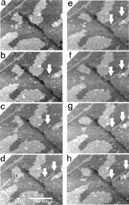
During the high-temperature anneal, the surface Bi reservoir is continuously depleted, with some Bi going to form nanolines, and the remainder evaporating back into vacuum. The activation barrier for evaporation is different for different surface adsorption sites. A RHEED studyMiki1999a found that the activation barrier for evaporation of Bi from the nanoline was 0.25 eV higher than the barrier for evaporation of Bi from a (2n):Bi overlayer. Hence Bi is mostly being lost from the background reservoir. However, it might be expected that missing dimers in the nanolines would be observed occasionally. In fact, this is not the case, and those nanolines which are observed at high temperatures always appear perfect. It is likely that, due to the large defect energy of the Haiku structure (0.66 eV from DFT calculationsWang2005 ), any Bi which evaporates from the nanoline is quickly replaced from the Bi reservoir. Thus at high temperatures, where Bi can evaporate from the nanolines, their stability is dependent upon a sufficient quantity of Bi in the reservoir to replace missing dimers. At the later stage of an anneal, no new Bi nanolines nucleate, and those which are present cease to grow. This is an indication that the reservoir of Bi is approaching exhaustion. Finally, when the reservoir is exhausted, evaporation from the Bi nanolines will take place, and they will disappear within a few scans, or sometimes within the time of one scan. A sequence showing the evaporation of nanolines is shown in Fig.16. In general, the nanolines evaporate from the ends, rather than breaking up into pieces, which strongly suggests that the ends of nanolines are less stable than the middle of the nanoline, and that the energetic barrier to break the nanoline in the middle and create two ends is prohibitive, even at these temperatures.
4.2.3 Promontory Growth
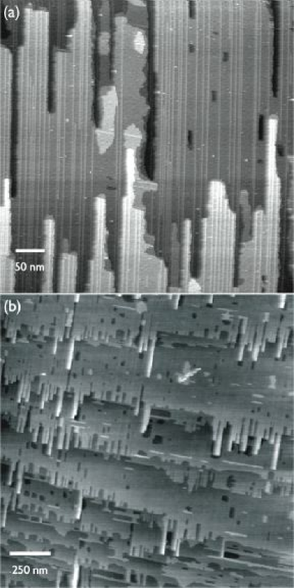
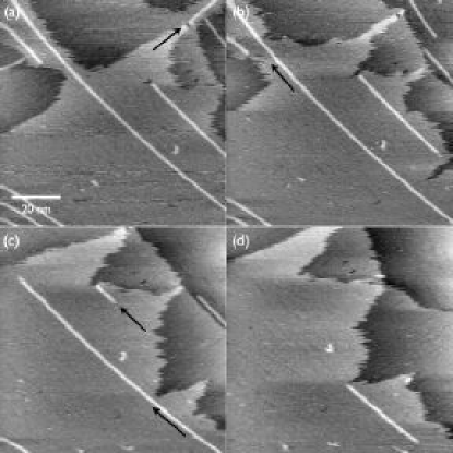
The most notable feature of the mature nanoline surface as seen in Fig. 11(c) and (d) as well as Fig. 12 is known as the promontory. Long, narrow islands of Si surrounding Bi nanolines grow out across lower terraces. A series of images showing the early stages of Bi nanoline growth are shown in Fig. 17. In (a), a short nanoline has grown out over a lower terrace and the joining of the promontory and the pre-existing step edge has formed a hole in the upper terrace, as is marked in (b). The growth of this promontory is blocked by the growth of a second nanoline, which has nucleated in the time interval between (a) and (b), and is growing out across the next lower terrace. Comparison of (b),(c) and (d) makes it it very clear that the promontories are the result of growth out over a lower step edge. By (d), a common pattern of zigzagging Bi nanolines which have blocked each other’s growth is developing.
The mechanism behind this promontory growth has not been determined; in an early paper, it was suggested that the promontories form by etching of Si around the Bi nanolinesMiki1999a . However, in Fig. 17, there is no sign of etching taking place; this is a pure growth phenomenon. It is likely that the growth of the nanoline is related to the high mobility of step edges at 500∘C. Nanolines will always continue to grow until they reach an obstacle. Thus nanolines will stop at step edges. However, the position of the step edge at this temperature is not constant; it fluctuates back and forthZandvliet1993 , as material moves randomly along it. This motion may be inferred from the jagged, streaky step edges in these high-temperature images, as discussed in Section 2.1. Therefore, each time the step edge moves forwards, the nanoline can extend to the new step position, and then when the step edge tries to move back again, its position is pinned by the presence of the nanoline. With each forward fluctuation therefore, the nanoline will grow forward, and thus a promontory will gradually form. A similar process could explain the retreat of an up step ahead of a growing nanoline. The notable feature of the promontory is that they have a fixed minimum width. At least 3-4 nm of Si is maintained on either side of the Bi nanoline. This fixed width is an example of the phenomenon known as the Defect Exclusion Zone, or ”DEZ”, which is discussed in Section 4.2.4.
4.2.4 The role of strain in surface interactions
Since the nanoline has a strain field associated with it, it is likely to exhibit quite strong interactions with other surface features which exert a localised strain on the surface. Such features might be adsorbed Bi dimers, missing dimer defects, step edges, and other nanolines.
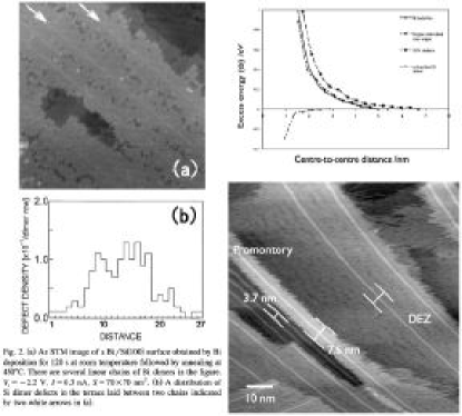
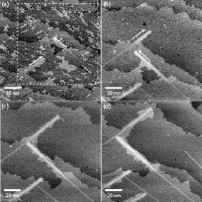
Using tight-binding simulations, where very large cells can be relaxed, the interaction between a nanoline and several features, such as 1DV defects and rebonded B-type step edges have been calculated. These data are plotted in Fig.18. From elevated-temperature STM images, it is clear that there is a repulsive interaction between the nanolines and missing dimer defects and step edges. At high temperature, as in Fig. 18, the surface is covered in black streaks, which indicate the positions of rapidly moving missing dimer defects. However, either side of the nanoline, there are no streaks. Likewise, where a nanoline forms a promontory, the width of this empty area is continued as the width of the promontory. This characteristic width of defect-free silicon, around 3-4 nm either side of the nanoline, is known as the “Defect Exclusion Zone” or DEZ Owen2004 . For a large separation, the total energy of a nanoline and a defect is the same as for the two structures independently. However, as the separation decreases, the total energy increases, so that at a distance of about 3.5 nm, there is a repulsive interaction between the nanolines of ca. 0.1 eV for both step edges and 1DVs, and at smaller distances, this energy increases rapidly. Statistics about the position of 1DVs in the space between two nanolines have been gathered, as shown in Fig. 18, taken from Ref. Naitoh1999 . They show that on average, most defects occur at least 3.2 nm away from the nanoline, which is in agreement with the calculated repulsion.
For a pair of nanolines, there is a similar interaction, and the 0.1 eV threshold is also reached when the centres of the two nanolines are about 3.5 nm apart, or in other words, the gap between the nanolines is the width of one nanoline. Clusters of nanolines with this approximate spacing are often seen, as in Fig. 18. For nanolines adjacent to each other, the excess energy is about 1 eV per unit cell. Despite this, nanolines are sometimes observed growing next to each other, as in Fig. 11(c). The reason for this is that unlike defects and step edges, which are mobile, a nanoline cannot move sideways. Hence when two nanolines which have nucleated in different places grow past each other, they cannot move sideways to reduce their interaction energy. The presence of nanolines in close proximity does indicate that this interaction energy is not so high as to present an insuperable barrier to the growth of two nanolines past each other. For Bi surface dimers, which have a compressive stress field, decoration of missing dimer trenches is a natural way in which to relieve their stress. The gain in energy by this process is about 0.45 eV/Bi dimer in tightbinding calculationsOwen2005b . The interaction with the nanoline is also attractive. In images where there is a large surface density of Bi dimers, they are often situated adjacent to the nanolines. This position is found to be 0.28 eV better in energyOwen2005b than elsewhere. This suggests that the nanolines are generally more stable in a surface with a significant amount of compressive stress, such as one which is covered in Bi. Indeed the energy of a nanoline in a Bi-terminated surface is 0.8 eV better than on a Si-terminated surface.
4.2.5 Nucleation
Despite the success of the Haiku structure in explaining all of the above surface phenomena, its identification raises as many questions as it answers. How would such a complex structure form? How is it terminated? If termination is energetically unfavourable, what would a nucleus structure look like?
Experimentally, the atomistic nucleation process remains a mystery. There is an incubation time during the annealing process before nanolines start to nucleate, which suggests that there is a significant barrier to formation of these structures. On many occasions, the appearance of Bi nanolines has been captured during STM observations, such as in Fig. 19. There is no apparent precursor state; like Athena from Zeus’ brow, a short nanoline springs fully-formed from an empty patch of the surface. The nanolines then grow extremely rapidly.
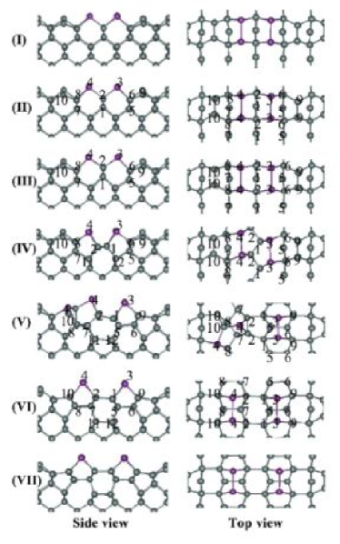
Thus far, there has only been one proposed mechanism for the nucleation of a Bi nanolineWang2005 . It has been suggested that the initial step is for Bi ad-dimers to fall into the missing dimer trenches on the hot Si(001) surface, forming a row of pairs of Bi dimers. Such a structure would result in the increase in local compressive stress, which may provide a driving force for nanoline nucleation. We demonstrated earlier (Fig.7) that the 7-5-7 structural motif may be achieved by a simple bond rotation process. Using this motif, the proposed mechanism suggests that the central four atoms between the two Bi dimers in the proposed mechanism twist, so that a zigzag core structure is formed. From this the Haiku structure evolves, with a maximum barrier in the calculation of less than 1.5 eV. The reaction pathway and associated energy diagram are shown in Fig. 20. This mechanism has a number of interesting features, but also a major limitation. The calculation takes place in a periodically repeated unit cell one dimer row wide, and is therefore considering the nucleation of an infinite nanoline, without ends. It is suggested that a long nucleus forms by the filling of several unit cells of a missing dimer trench, but this is an unstable situationOwen2005b . Moreover, in our STM observations, we observe the appearance of very short nanolines, which then grow. The termination of these finite nuclei must therefore be considered. STM observations of nanoline evaporation show that nanolines do not break up in the middle, instead they evaporate from the ends. From this, it may be inferred that the energy of termination is quite high. While there has been no systematic study of termination, we have performed calculations on many and varied structures, all of which have been found to have a high energy. In tightbinding modelling, the energies were at least 1 eV/end , while those terminations which we have considered for the proposed zigzag nucleus structure have much higher energies, around +1.6 eV/end, giving a total nucleus energy of over +4 eV. This suggests both that understanding the termination of the nanolines is an important area for future research, and that nucleation structures should be considered in 2D, rather than in 1D (which may not be feasible with a technique more accurate than tightbinding). Given that the prevalent structures on the Bi-rich surface are Bi surface dimer/1DV complexes, alternative nucleation mechanisms which use these structures as a basis may be more fruitful and are being explored.
4.3 Electronic Structure
The knowledge of the electronic structure of the Bi nanoline has stemmed from two sources: variable-voltage STMMiki1999a ; Owen2003 ; MacLeod2005 and DFT calculations of the electronic structureSrivastava2004 ; Owen2002b ; Bowler2000 ; Miwa2002a ; Bowler2002 ; Miwa2002b ; Owen2003 ; MacLeod2005 ; Miwa2005b (generally considered in terms of the local density of states (LDOS), or the Tersoff-Hamann approach to STM, which uses the LDOS). Knowledge of the atomic structure of the Bi nanoline allows detailed calculations of its electronic structure to be made, which can then be compared to the observations made in STM. While the majority of the electronic contrast is expected to be dominated by the Bi dimers in the nanoline, other details of the LDOS have allowed a stronger identification of the Haiku structure with the Bi nanoline to be made, with the other possible candidate structures ruled out after comparison with the STM data.
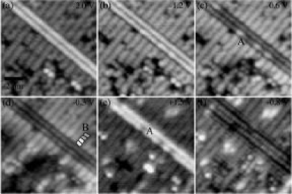
We begin by summarizing the data available from STM, which is illustrated in Fig. 21:
-
1.
At high biases, the Bi nanolines appear bright compared to the surrounding Si(001) surfaceMacLeod2004a ; MacLeod2004b ; Miki1999a ; Miki1999b ; Naitoh1999 ; Naitoh2000 ; Owen2005b ; Owen2002b ; Owen2003 ; MacLeod2005 ; Miwa2005 ; Naitoh1997 ; Naitoh2001
-
2.
At low biases, the Bi nanolines become dark compared to the surrounding Si(001) surfaceMiki1999a ; Miki1999b ; Owen2005b ; Owen2003 ; MacLeod2005
-
3.
At low biases, the Si dimers neighbouring the Bi nanoline show enhancement, or brighteningOwen2003 similar to that seen around missing dimer defects on Si(001)Owen1995 ; Schofield2004 .
These facts suggest various things: first, that the Bi dimers are physically higher than the surrounding Si(001) surface dimers, as at high biases the contrast in STM is determined primarily by geometrical structure; second, that the local electronic structure of the Bi dimers will show states further from the Fermi level than the surrounding Si dimersOwen2003 ; MacLeod2005 ; Miwa2005b , as this determines the STM current at low biases; finally, that the Bi nanoline structure must be under tensile stress, which causes the Si dimers near the nanoline to be pulled together, away from their relaxed surface structure, which is the origin of enhancement at low biasesOwen1995 ; Schofield2004 .
4.3.1 Electronic Properties of the Bi dimer
Examination of the detailed electronic structure of the Miki and Naitoh modelsMiwa2002a ; Miwa2002b ; Srivastava2004 and the Haiku structureOwen2003 ; Owen2004 ; MacLeod2005 all show that the Bi dimers become dark at low bias voltages by contrast to the surrounding silicon dimers. The calculated DOS for the Miki and Haiku structures are shown in Figure 22Miwa2005b . The peak comes from the up atoms of the substrate Si dimers, as does the , while the peak comes from both the Bi and Si dimer bonds and from the Bi atoms in the line models. When the substrate dimers are passivated with H, the peaks and almost disappear leading to peaks in the gap which arise from the Bi dimers ( and ). This data confirms earlier modelling and bias-dependent STM measurementsOwen2003 discussed below.
Consideration of the electronic structure of the Bi dimer reveals that it is rather unusual. In its native form, Bi forms puckered hexagonal sheets, similar to the structure taken by As. Full-potential LAPW modelling of Bi in a bulk diamond cell (thus forcing it to take up tetrahedral bonding) showed that there is very little hybridisation between the s- and p-orbitalsBowler2000 . Thus we expect Bi to tend towards p3 bonding with a filled s-orbital (as a lone pair) and to be energetically most favourable with 90∘ bond angles. This explains to some extent the Haiku structure, where bond angles are almost 90∘. Projection of the local densities of states calculated using pseudopotential-based DFT calculationsMacLeod2005 suggests that the Bi dimer in the Haiku structure has hybridisation between s and pz, with px and py separated off. The FLAPW calculations showed that the relativistic effects of the full core increased the s-p splitting in the Bi atom; while relativistic effects can be incorporated in pseudopotentials, the Haiku structure might be more stable, and show bonding closer to p3, if these effects were taken fully into account444We note that a full potential calculation on a unit cell large enough to hold the haiku structure is probably computationally prohibitive.
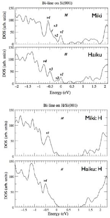
The Bi-Bi bond is a rather weak bond, with the Bi-Si bonds providing most of the energetic stability. This can be seen by considering the electronic structure of a Bi ad-dimer on the clean surface555While not a perfect mimic of the Bi dimer in the Haiku structure, the smaller cell allows more detailed calculations to be made.. The electron localisation function (ELF)Becke1990 for this ad-dimer is shown in Figure 23(a)Bowler2005 . The ELF gives a quantitative analysis of the bonding properties of a system, with a value of 0.5 equivalent to the localisation seen in the homogeneous electron gas and a value of 1.0 equivalent to complete localisation. The figure shows an isosurface with ELF=0.8 (equivalent to reasonably strong covalent bonds). It can be seen that the Si-Si bonds are rather strong, as expected, and that the Bi-Si bonds are still visible at this level, though they are weaker than the Si-Si bonds. The Bi-Bi bond is not visible (in fact it has a maximum value around 0.7) but the Bi lone pairs are visible as rather diffuse, spherical objects (by comparison to the up atoms of the substrate dimers). This implies that the Bi-Bi bond is rather weak, and the lone pairs would not be available for bondingBowler2005 . The energy barrier to breaking the bond in this Bi dimer has been calculated with DFT to be 0.17 eV going from over the dimer row to over the trench between rows and 0.15 eV going in the other direction, and the barrier is shown in Fig. 23(b). Having the Bi dimer over the dimer row is more stable than over the trench between rows by about 0.02 eV. This implies that there should be a finite chance of imaging the Haiku structure with the Bi dimers out-of-phase with the underlying Si dimer rows. However, we note that with the energy difference noted above, the dimer would be over the row 98% of the time at room temperature, and the likelihood that a whole line of dimers would flip, will be even smaller. There are occasional images with the dimers out-of-phase, but these are rare.
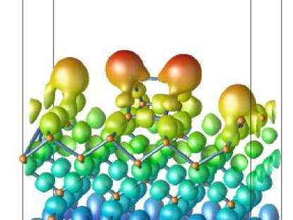
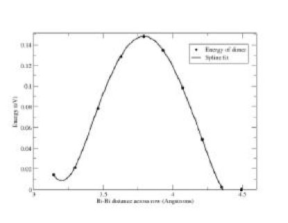
In the next section, details of some elements which will attack the Bi-Bi bond will be presented, along with others that will not. Here we consider the local structure of the bond. When the Bi-Bi bond is over the Haiku core, it is almost perfectly relaxed, with bond angles extremely close to 90∘. Insertion of any species into the Bi-Bi bond will distort these angles (and the angles formed with the underlying Si atoms), with a potentially large energy penalty. Thus the Bi-X-Bi angle should be relatively close to 180∘ with short Bi-X bond lengths if an element X is to insert successfully into the bond. Furthermore, the lone pair on the Bi dimer, which might be expected to be a strong electron donor, is in fact rather passive, as it lies some distance below the Fermi levelBowler2005 . The implications of this for the chemical reactivity of the Bi nanoline are discussed below in Section 4.4.
4.3.2 Strain-induced Enhancement
The phenomenon of strain-enduced enhancement at low STM bias voltages has been explored beforeOwen1995 ; Schofield2004 ; we reproduce the arguments here for convenienceOwen2003 . The Si(001) surface shows a dimer reconstruction which provides three bonds per surface Si atom (compared to two bonds per atom for the bulk terminated surface), but which pulls the bond angles and distances away from the ideal tetrahedral values. The net result is that the local band gap is reduced (in simple chemical terms, the hybridisation towards sp3 is decreased, leading to a decreased splitting between the resultant hybrid bonds). If the surface dimers are then further distorted, their local states will move closer to the Fermi level. The single missing dimer defect (1DV) has second layer atoms bonding across the defect which distorts the dimers either side of the defect (though lowering the energy because the second layer atoms have no dangling bonds). This distortion in turn causes the states near the Fermi level on the neighbouring dimers to move towards the Fermi level, leading to a brightening or enhancement at low biases.
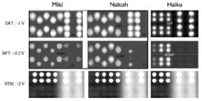
Low-bias simulated images of the Naitoh and Miki structuresMiwa2002b ; Miwa2002a ; Srivastava2004 show that the Si dimers adjacent to the Naitoh become darker than the surrounding Si dimers as the Fermi level is approached, while those on the Miki model are unchanged. By contrast, with the Haiku structure, the Si dimers immediately adjacent to the nanoline become brighter closer to the Fermi levelOwen2003 ; Owen2004 , in good agreement with the STM images. A comparison of high and low-bias simulated images of the 3 structures are shown in Fig. 24. However, the prediction from the Miki model does agree very well with the appearance suggested from STM imagesMiki1999a ; Naitoh2001 , in which the shoulder dimers around a 1DV on a Bi-rich surface become dark at low bias voltages. On the basis of these calculations, we suggest that the lack of enhancement at low bias voltages indicates almost complete relaxation of the strain of the 1DV by the presence of the Bi dimers in the Miki model.
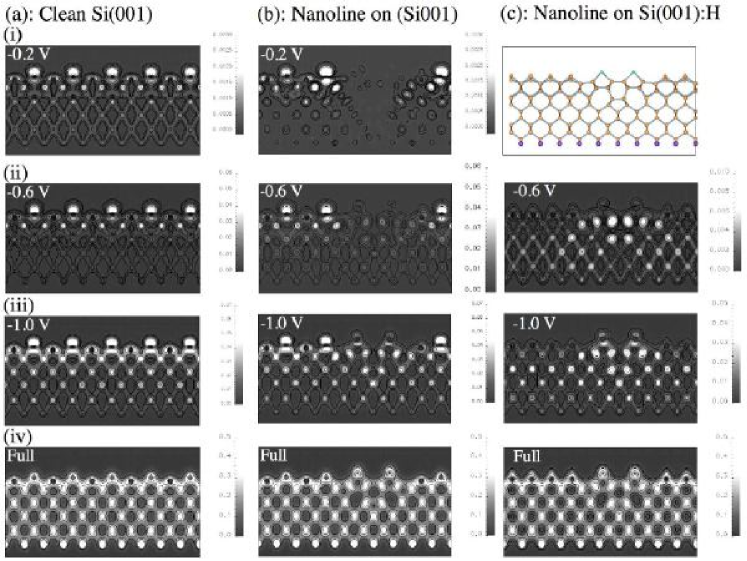
Taking the principle of strain-induced enhancement further, the local subsurface strain could be determined by cross-sectional STM of the Bi nanoline, of which there is none, or from LDOS calculations, by projection of the charge density on a plane perpendicular to the (001) surface. We show the projected charge density from GGA calculations for the clean Si(001) surface, the Haiku structure and the Haiku structure with hydrogen on the Si(001) surface in Fig. 25Owen2003 , on the (10) plane, parallel to a Si dimer row. By comparing in particular the clean Si(001) surface and the clean Haiku structure, the change in different states induced by the Haiku can be seen. Beginning with the clean surface, the localisation of the states close to the Fermi level in the top few surface layers shows the strain induced by dimerisation. In the Haiku structure, these states are even more strongly localised on the dimers immediately adjacent to the Haiku structure, which causes their relative enhancement in STM. Meanwhile the triangular Si substructure of the Haiku, c.f Fig. 8, is somewhat relaxed compared to the clean Si dimers, although it is strained relative to the hydrogenated dimers and perfect bulk Si. This goes some way to explaining the stability of the subsurface 5-7-5 ring structures, which serve as a highly effective relief mechanism for the epitaxial stress exerted by adsorbed Bi. The absence of states close to the Fermi level suggests that the nanolines are likely to block surface conduction perpendicular to the nanoline, and are not likely to act as a nanowire.
The lack of any states on the Bi near the Fermi level is clearly the cause of the darkening of the nanoline relative to the Si(001) surface seen in STM at low voltages. In the full charge densities(Fig. 25(iv)), the density of states associated with the Bi dimers, combined with their higher physical height, explains their relative brightness in STM at higher bias voltages. In the case of the hydrogenated surface, the Bi dimers have a similar charge density as in the clean surface, but in this case, the Si -bonds have been eliminated, so the Bi dimer remains bright in STM at all biasesOwen2002a .
4.4 Chemical Properties
As described above in more detail, the bonding orbitals in the Bi dimers have essentially a p3 bonding character, while the lone pair is a diffuse s-type orbital, some 10 eV below the Fermi levelBowler2000 . Thus the Bi dimer is in a very stable electronic state, and is not expected to be very reactive. Moreover, this low-energy configuration is dependent upon the maintenance of bond angles close to 90∘, which will have an effect on the energetics of any insertion into the Bi-Bi dimer bond. However, the low-bias images shown above reveal that although the nanoline appears clean at high biases, some contrast between different dimers is visible at lower biases, suggesting that some chemical attack has occurred.
4.4.1 Reactivity of the Bi dimer
We have proposed that the Bi nanolines, although semiconducting themselves, might be used as templates for deposition of other materials, such as metals, active molecules, nanoparticles etc.Owen2002a ; Owen2005c . In order for the nanoline to have utility in this role, it must be possible to mask the substrate around the nanoline, so that adsorbants stick preferentially to the nanoline. It is also important, for any nano-electronics applications, to have some method for rendering the substrate insulating after growth of the nanoline. The chemical reactivity of the Bi dimers, and the nanoline as a whole, is therefore crucial to any implementation of this concept. Atomic hydrogen has been used as a mask on the bare Si(001) surface for STM lithography experimentsHashizume1996 ; Shen1997 ; Sakurai2000 , in which an STM tip is used to remove lines or areas of hydrogen from the surface, and thus provide areas onto which metal will adsorb, as in Fig. 2. However, the writing process is slow, and lacks scalability. Use of the Bi nanolines as templates would remove the need for this writing, while providing long, and more uniform patterns. Hydrogen is therefore a natural species to use as a mask around a Bi nanoline.
One of the most favourable properties of silicon as an electronics material is the high quality of its oxide film. Oxidation of the silicon around the Bi nanoline is therefore a natural way in which to isolate the nanoline electrically from the substrate. The usual method of oxidation of silicon is by exposure to molecular oxygen or to water at elevated temperatures, but this only gives microelectronics-quality oxide when grown at ca.800∘C. Since the Bi nanoline is not stable above 600∘C, ozone was considered as an alternative for low-temperature oxidation. Ozone preferentially attacks the backbonds of the surface Si dimers, forming a stable oxide, even at room temperatureNakamura1999 . More recently, the need for high-k dielectrics has driven the development of silicon nitride and oxynitride as alternatives to silicon dioxide. Nitridation is usually done using ammonia, which breaks up on contact with the clean silicon surface above 200 KRignanese2000 . As an added bonus, when ammonia reacts with silicon, the nitrogen moves below the surface, but the hydrogen remains on the surface, passivating it. It can therefore play a dual role, as insulating reagent, and as masking material. The reaction of these species with the Bi nanoline are discussed in the sections below.
4.4.2 Hydrogen
The Bi nanoline has been shown to be almost completely inert to attack by atomic hydrogenNaitoh2000 ; Owen2002a ; Owen2005b . Fig.26(a) shows a close-up image of a nanoline on a Si(001):H monohydride surface. In this image, nanolines were formed at 590∘C, and the surface was cooled to 330∘C, the surface was saturated with atomic H. The surface has the monohydride phase, with the Si-Si -bond intact, and the H atoms saturating the dangling bonds. Thus each Si-H dimer is resolved as a pair of dots. Some white dots on the Si surface may be holes in the monohydride layer, stray bismuth atoms, or adsorbed -OH resulting from water impurity in the hydrogen. While the nanoline is almost completely unreacted, one dimer has become dark. This sort of defect is extremely rare. The preferential adsorption of the H onto the Si is consistent with DFT-LDA modelling, which found that H on a Bi dimer is 3 eV worse than H on a Si dimer. There is therefore a strong driving force for any H which does adsorb onto the Bi nanoline to diffuse off it, and onto the Si.
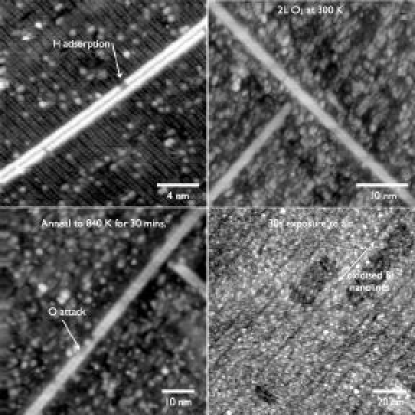
4.4.3 Oxygen
The oxidation properties of a monolayer of Bi on Si(001) shows an unusual changeover in behaviour with oxygen exposure. An EELS/Auger studyKoval1997 found that for small exposures, the reactivity of a Bi overlayer on Si(001) is 100 times less than the reactivity of oxygen with the bare silicon surface. However, for large exposures, above ca. L O2, the oxygen Auger intensity continues to increase for a Bi/Si(001) surface, at a point where the signal for the clean Si(001) surface has saturated. Thus for very large exposures, the Bi promotes oxidation of the silicon. Moreover, the stoichiometry of the oxide formed on the Bi/Si(001) surface is closer to SiO2, which would imply better insulating properties. Semiempirical calculations found that insertion of oxygen into the Bi-Bi bond is energetically much less favourable than for Sb or As (0.32 eV vs ca. 4.7 eV). Moreover, insertion into a Bi-Si bond or a Si-Si bond is much more favourable (4.5 eV and 5.5 eV respectively), so that preferential attack of the silicon is expected.
The reactions of molecular oxygen and ozone with the Bi nanoline show a similar changeover in behaviourOwen2002a . The surface was exposed to ozone at room temperature and, for comparison, to molecular oxygen at 400∘C. Both surfaces were annealed up to 570∘C, near the stability limit of the Bi nanoline. The room-temperature ozone experiments, using exposures up to 20 L of O3, revealed that the silicon background could be saturated without visible damage to the nanoline. In large-scale images, the Bi nanoline appears to be completely unaffected, as shown in Fig. 26(b). However, in small-scale images, and by varying the imaging bias, some subtle differences between the appearance of various dimers in the nanoline could be seenOwen2002a . This variation may be due to attack of Bi-Si backbonds, as found to be favourable in MNDO simulationsAfanasieva2002 , which would leave the Bi-Bi dimer intact, but perturb its electronic structure somewhat. Annealing this surface introduced some defects into the nanoline. After annealing at 450∘C, gaps appear in the nanoline, which comprise 1-2 unit cells. This trend continued with a further anneal to 570∘C, as shown in Fig. 26(c). Such piecemeal damage may be explained by the observation that the activation barrier for Bi to desorb from oxidised Si has been found to be 0.7 eV lower than for unoxidised SiKoval1997 . The small contrast changes, which were seen after ozone exposure at room temperature may therefore indicate reaction with Bi-Si, or Si-Si backbonds around the nanoline, so making that unit cell more susceptible to evaporation during high-temperature annealing. Molecular oxygen, when adsorbed at 400∘C, behaved in a very similar way to ozone. Again there was preferential attack of the silicon, leaving the nanoline mostly intact, but also gaps appeared in the Bi nanoline after annealing for about one hourOwen2002a .
While the Bi nanoline is remarkably resistant to oxidation in UHV, it quickly oxidises when exposed to air, as shown by the following simple experiment. A H-terminated Si(001) surface with Bi nanolines was taken out of the imaging chamber into the UHV system loadlock, which was then vented to atmosphere for 30s, and then immediately pumped back down to UHV. The resulting surface is shown in Fig. 26(d). The nanolines, which previously were bright at all biases relative to the H-terminated background, are now black lines, indicating that they have suffered significant attack. This agrees well with the previous study, which found that for very large exposures to oxygen, the Bi dimers promoted oxidation of the underlying silicon.
4.4.4 Ammonia
The adsorption of ammonia onto Si(001) as a precursor to silicon nitride or oxynitride growth has been studied by a variety of experimental and theoretical techniques, which concluded that at room temperature, the ammonia dissociated on the surface, forming NH2 and H groupsRignanese2000 . We have found that ammonia attacks the silicon preferentially at room temperature. An image of the Bi:Si(001) surface with ammonia termination is shown in Fig.27. Within each dimer, the light grey end has been identifed with the NH2 group, while the dark grey end is the H atomOwen2005a . The apparent height difference in STM matches the physical height difference between these two species. There is some ordering of the NH2 groups, such that zigzag patterns and straight lines are seen running along the dimer rows.
Reaction of ammonia with the Bi nanoline might be expected to proceed by the initial formation of a hydrogen bond between an ammonia H atom and the Bi lone pair, followed by insertion into a Bi-Bi or Bi-Si bond. However, as discussed above, the lone pair on the Bi dimer is essentially inertBowler2005 . During experiments on a surface which was pre-exposed to atomic H to saturate the Si dangling bonds, for exposures of up to 70L of ammonia at substrate temperatures of up to 500K, the Bi nanoline was largely unaffected. However, adsorption of ammonia onto a Bi nanoline surface where the Si dimers are not passivated does result in some reaction with the nanoline, even at room temperature. This difference may indicate that ammonia reacts first with the silicon, forming active NH2 species, which are mobile and can attack the Bi dimers. Calculations suggest that it is energetically favourable for an NHx group to insert into the Bi-Bi dimer bond, and form a symmetrical Bi-NH-Bi feature. However, STM images of reacted Bi dimers shows an asymmetric feature, not unlike the feature seen on background Si dimers. Examples may be seen in the inset to Fig. 27. Nevertheless, the probability of attack by ammonia is low, providing the promise that ammonia can be used to grow silicon nitride without damage to the nanoline.
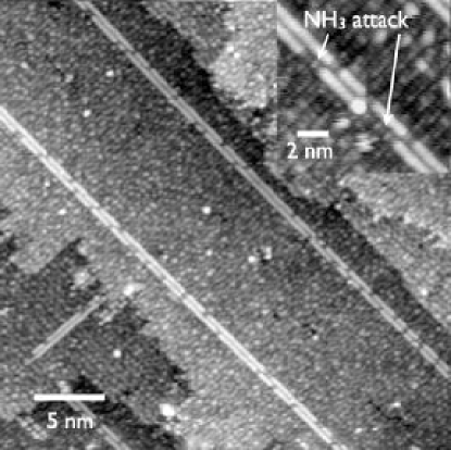
4.4.5 Metals
Metal deposition onto the Bi nanolines is currently under investigation. Deposition of Ag onto Bi nanolines on the clean Si(001) surfaceItoh2005 reveals a strong preference for adsorption onto the Si, leaving the Bi nanoline clean (in complete contrast to the behaviour of ErSi2 NWs on Si(001) discussed above in Sec. 3.3). However, the passivity of the Bi nanolines to atomic hydrogen and ammonia allows these species to be used as nanoscale masks. Ag is known not to adsorb onto H-terminated Si(001)Sakurai2000 as shown in Fig. 2, while In completely dewets from the Si(001) surface, forming large droplets when H is adsorbed onto an In-covered surfaceZotov1997 . In all cases, following metal deposition onto an ammonia-terminated Si(001) with Bi nanolines, preferential adsorption onto the Bi nanoline (or onto background Bi) was seen, indicating that the ammonia-terminated surface is very effective as a mask against metal deposition. The reaction of the metal with the nanoline template is more complex, however. Two types of behaviour have been seen with different metals, which may be described as wetting and non-wetting behaviour. Wetting occurs when the interaction of the metal with the nanoline is stronger than the interaction of the metal with itself. Nonwetting occurs when the interaction of the metal with itself is stronger. Examples of each type of behaviour for different metals, In and Ag, are shown in Fig. 28. Adsorption of In results in significant intermixing of In and Bi, forming a zigzag island structure, which is thought to result from a chain of In and Bi atoms, as shown in the inset to Fig. 28(a). Second-layer islands have a distinctive bright hexagonal feature, which is 19 Å or 2.5 dimer rows wide. This rational relationship between the In island dimension and the underlying Si unit cell distance demonstrates that these In islands grow epitaxially on the nanoline template, raising the possibility of the growth of long single-crystal nanowires on the Si(001) surface. By contrast, adsorption of Ag results in the formation of small clusters of Ag, around 0.5 nm in height, at a very early stage of deposition, as shown in Fig. 28(c). Further deposition at room temperature results in an increase of the number density of these nanoclusters, but the modal size increases only slightly from 0.5 nm to 0.6 nm, with a strongly peaked height distribution. This behaviour may be thought of as non-wetting behaviour.
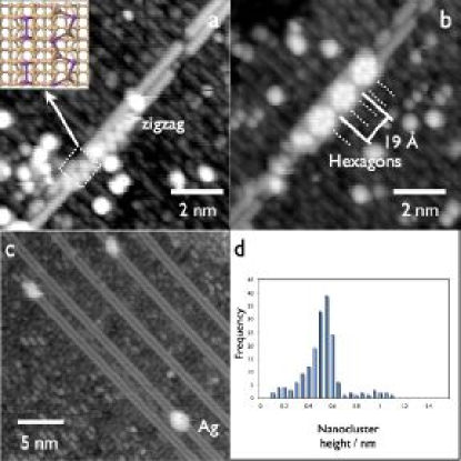
4.5 Burial
While the Bi nanoline has a number of interesting properties, for any nano-electronics device application it must be possible to passivate them against atmospheric attack. One way in which to do this is to bury them in a layer of epitaxial silicon. Moreover, the burial of the Bi atoms may lead to their acting as a 2D delta-doping layer, with close to atomic-layer precision in the depth placement. However, as with other nanostructures, for example burial of InAs/GaAs quantum dots in GaAs, the process of burial is likely to change the shape and detailed structure
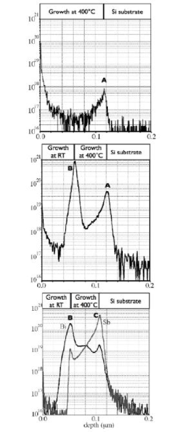
Simple overgrowth of a surface containing Bi nanolines results in the destruction of the nanolinesMiki1999c ; Yagi2005 . As shown in the Secondary Ion Mass Spectrometry(SIMS) profile in Fig. 29(a), after overgrowth of Si the vast majority of the Bi has segregated to the surface of the grown film, although there is a small peak in the Bi concentration at the original surface position. Furthermore, X-ray analysisYagi2005 shows that the 1-D character of the nanoline is lost after capping, even by an amorphous overlayer deposited at room temperature. The mechanism by which the Bi floats to the surface during growth is thought to involve exchange of subsurface Bi atoms with surface Si atoms, as Bi is an effective surfactant during growth. In order to prevent this, a further surfactant layer of Bi can be deposited around and over the Bi nanolines, before Si overgrowthMiki1999c . In this case, the exchange mechanism is inoperative, as the second-layer Bi in the nanolines will not exchange with first-layer Bi, and so it is possible to block the segregation of the Bi nanolines to the growth surface. In the SIMS profile in Fig. 29(b), a thin crystalline Si overlayer has been grown at 400∘C after deposition of a Bi layer, and this has been capped by depositing further Si at room temperature, so as to bury the growth surface in amorphous Si. In this case there, are two peaks in the SIMS profile. ‘A’ refers to the Bi density at the original Bi nanoline surface, while ‘B’ refers to the surface of the crystalline overgrowth. The surface of the overlayer has approximately 1 ML of Bi on it, from which the quantity of buried Bi can be determined. This is approximately 5% ML, which is typical for a Bi nanoline surface. Thus, using the Bi surfactant layer, most of the Bi nanolines have been preserved at the original surface. In order to gain more information about the exchange process, a surfactant layer of Sb was also used, instead of the surfactant layer of Bi. The resulting SIMS profile is shown in Fig. 29(c). In this case, there is a large peak of Sb at the original nanoline surface position ‘B’, while a considerable fraction of the Bi has segregated to the surface of the overlayer ‘C’. This result indicates that there is considerable exchange between the Sb surfactant layer and the Bi nanolines, and by this method, a layer of Sb has been successfully buried, with a sharp peak at the original nanoline surface.
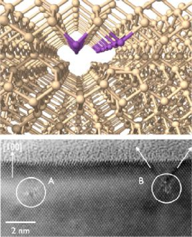
While this exchange process is successful at burying the Bi atoms, it does not provide any information about the structure of the buried Bi. For device applications, it is important to retain the 1-D character of the original nanoline. It is also of interest whether the Haiku structure will be preserved. STM cannot observe subsurface features, and instead the structure of the buried Bi nanolines was studied using an X-ray methodSakata2004 . The results of this analysisSakata2005 indicate that two important elements of the Bi nanoline structure have been preserved: the 1-D character, and the dimerisation of the Bi atoms. Tightbinding and DFT calculations of the buried Bi nanoline structure found that the Haiku structure was not stable, and broke down into a hollow 1-D structure with Bi dimers bonding to the silicon grown over the nanoline, and the Si substructure reconstructing into something similar to a 2DV surface defect. A ball-and-stick model of this proposed structure is shown in Fig. 30(a). It has significantly lower energy per Bi atom than other proposed structures, including substitutional and interstitial Bi defects. This structure may be compared to the cross-sectional TEM image of buried Bi nanolines in Fig. 30(b). Two nanolines are present within the TEM image. The one on the left has strain associated with it, and a dark core, which may match with the proposed structure. The one on the right has triggered misfit dislocations along {111} planes, c.f. Fig. 8. These dislocations, which indicate the presence of a large local stress, may suggest that the Haiku substructure of the nanoline has survived overgrowth. A recent X-ray Standing Wave (XSW) study of a Bi nanoline sample which had been capped with amorphous Si at room temperatureSaito2003 has cast doubt on the validity of the Haiku model. However, more detailed analysis of lines buried with amorphous siliconSakata2005 showed that the dimerisation and one dimensional character of the nanolines is destroyed by burial in amorphous silicon (and, as discussed above, burial in crystalline silicon changes the Haiku reconstruction while leaving the one dimensional, dimerised character of the nanolines unaffected). Furthermore, the presence of a significant quantity of Bi at the growth surface may have an effect on the results obtained, unless it is removedYagi2005 .
5 Conclusions
We have given a broad overview of the different material systems and experimental methods which result in self-assembled 1D nanostructures on semiconductor surfaces, particularly the technologically important Si(001) surface. There are many different self-organising systems which result in 1D nanoscale features on the surface of Si(001) and Si(111). Aside from the Pt/Ge(001) system, none of these approach the length, and degree of perfection, of the rare-earth silicide wires and the Bi nanolines. The metal/Si(111) nanowire systems will tend to form 3 equivalent domains, limiting the long-range order of the nanowires, while the methods which rely on step-edge adsorption are limited by the spacing of step kinks (though this can be controlled with careful sample preparation). The rare-earth silicide nanowire family are not nanowires per se (in that they are a metastable state, not seen in a bulk structure), but are better regarded as a conventional heteroepitaxial system in which the lattice mismatch is anisotropic. Even so, while many different rare earths superficially appear to behave in a similar fashion, review of the literature indicates that in fact several different nucleation and growth mechanisms are responsible for the formation of nanowires within this family, both kinetic and thermodynamic. The recent observation of nanowires with an orthorhombic crystal structureHarrison2005b , rather than the hexagonal structure previously reported, suggests that there is much more to be learnt about this family of materials. Experimental studies of all these systems has so far been largely confined to STM, apart from X-ray and TEM studies of buried Bi nanolines, and TEM of the endotaxial RE nanowires. A much greater understanding of the physical, chemical and electronic properties of these systems, would come from other experimental techniques, such as optical and vibrational spectroscopic techniques. (For example, the strained Haiku core of the Bi nanoline may have a signature bond vibration frequency.)
The main focus of this review has been the Bi nanoline system. We have described the physical and electronic structure of the Bi nanoline, its reactivity with different materials, and the surface phenomena associated with it. Although there has been no direct observation of the core structure of the Haiku model, it provides a natural explanation for all the observed experimental phenomena, and is well-supported by experimental and theoretical data. The fundamental source of many of the properties of the Bi nanoline is the subsurface core of Si which has recrystallized into a hexagonal phase, Lonsdaleite (known from meteorites). The formation mechanism of this core structure remains unknown. A significant activation barrier is expected, given the high temperature and long incubation time required to form the nanolines, and the co-existence of the nanolines with the Miki structure, which is less stable, but kinetically easy to form. While mechanisms proposed thus far have concentrated on the twisting of pairs of atoms, an alternative may well be a stacking-fault-like shift of the entire core from the cubic phase to the hexagonal phase. Given their structure, it is clear that the Bi nanolines are not a conventional heteroepitaxial system like the silicide family. There is no variation in width, either with annealing temperature or time – only the number density of nanolines and the length changes with further deposition and annealing. The nanolines are only ever one unit cell wide, although clusters of nanolines are sometimes seen. The nanolines are not the result of simple adsorption onto symmetry-breaking features of the surface, such as step edges, or linear defects. Nor are they a periodic reconstruction of the surface, as in the Pt/Ge wiresGurlu2003 . They might best be described as an adsorbate-stabilized surface recrystallization.
The chemical properties of the nanoline stem from the behaviour of the Bi dimer with its preference for p3 bonding and an inert s-type lone pair, rather than the sp3 hybridization of Si dimers. Although the Bi-Bi bond is weak, it is also passive, and only In shows any significant reaction with it, probably because the zigzag structure produced allows the Bi atoms to retain their preferred 90∘ bond angles. Hydrogen does not attack the Bi nanoline, while ozone will oxidise around the nanoline at room temperature, leaving it intact. Likewise ammonia preferentially attacks the silicon, although some damage to the nanoline occurs at small fluxes.
The determination of both the physical and electronic structure of the nanoline has demonstrated the importance of a close interaction between experiment and theory. We note that all the recent publications on the Bi nanoline have been a collaboration between the two. The method of tightbinding has proved to be a valuable tool for quickly searching through a large variety of possible structures, as in for instance the Haiku structure, or for relaxing a large number of atoms, as in modelling of the nanoline kink energies. At the same time, the tightbinding method retains a quantum mechanical description of the energetics, so that the calculated energies are in most cases in reasonable agreement with those calculated using DFT. The Bi nanoline has benefitted from an unusual degree of theoretical investigation. A similar level of theoretical work for the rare-earth nanowires is likely to deepen greatly the understanding of the different nucleation and growth phenomena that have been identified in that family of systems.
With a significant body of work devoted to the fabrication and structure of the nanoline systems, attention should be paid to their possible applications. The length, straightness and perfection of self-assembled nanolines lend themselves to use as a nanoscale template. The most obvious candidate systems are the rare-earth nanowires, which are themselves metallic, so that an array of parallel nanowires would readily form the contacts for a nanoelectronic device, perhaps using the “crossbar” architecture. The Er silicides appear also to act as preferential adsorption sites for metals such as Pt, so that the properties of these contacts is not limited to that of the nanowires themselves. However, the growth of these nanowires on a semiconducting substrate, with no indication as yet that the substrate could subsequently be oxidised, might limit their application in nanoelectronics (for which a high-quality insulating substrate is crucial). For the Bi nanolines, oxidation of the surrounding silicon with ozone, followed by passivation of the surface with hydrogen, or nitridation using ammonia, is a plausible route for the fabrication of a single-nm 1D template on an insulating surface, considerably smaller than any of the rare-earth nanowires, and well within the size range where quantum scale effects might be expected to occur. By the deposition of metals, active molecules, nanoparticles, or other species onto this template, the fabrication of nanowires, or arrays of nanoparticles with interesting optical, electronic or magnetic properties could be achieved, with atomic precision. This area is being actively pursued by the authors.
Acknowledgements.
We are happy to acknowledge useful discussions with Chigusa Ohbuchi and Wataru Yashiro, as well as permission from various authors to reproduce figures as noted in the text. This study was performed through Special Coordination Funds for Promoting Science and Technology from the MEXT, Japan (ICYS and Active Atom-Wire Interconnects). DRB is funded by the Royal Society.References
- (1) D.R.Bowler J. Phys. Cond. Matt. 16 (2004) R721.
- (2) J. V. Barth, G. Costantini and K. Kern Nature 437 (2005) 671.
- (3) W.Chen and H.Ahmed Appl. Phys. Lett. 62 (1987) 1499.
- (4) T. Hashizume, S. Heike, M. I. Lutwyche, S. Watanabe et al. Jpn. J. Appl. Phys. Pt. 2 35 (1996) L1085.
- (5) J.R.Heath, P.J.Kuekes, G.S.Snider and R.S.Williams Science 280 (1998) 1716.
- (6) J.Nogami, S.L.Park and C.F.Quate Phys. Rev. B 36 (1987) 6221.
- (7) O. Gurlu, O. A. O. Adam, H. J. W. Zandvliet and B. Poelsema Appl. Phys. Lett. 83 (2003) 4610.
- (8) M.Naitoh, H.Shimaya, S.Nishigaki, N. Oishi et al. Surf. Sci. 377-379 (1997) 899.
- (9) K.Miki, J.H.G.Owen, D.R.Bowler, G.A.D.Briggs et al. Surf. Sci. 421 (1999) 397.
- (10) A. A. Baski, K. M. Saoud and K. M. Jones Appl. Surf. Sci. 182 (2001) 216.
- (11) C. Preinesberger, S. Vandré, T. Kalka and M. Dähne-Prietsch J. Phys. D: Appl. Phys. 31 (1998) L43.
- (12) K.Sagisaka, D.Fujita and G.Kido Phys. Rev. Lett. 91 (2003) 146103.
- (13) O. Kubo, J. T. Ryu, H. Tani, T. Harada et al. Appl. Surf. Sci. 169 (1999) 93.
- (14) J.T.Wang, H.Mizuseki, Y.Kawazoe, T.Hashizume et al. Phys. Rev. B 67 (2003) 193307.
- (15) J. Wang, E.G.Wang, D.S.Wang, H.Mizueki et al. Phys. Rev. Lett. 94 (2005) 226103.
- (16) C. J. Chen Introduction to Scanning Tunneling Microscopy Oxford Series in Optical and Imaging Sciences Oxford University Press (1993).
- (17) R. Weisendanger Scanning Probe Microscopy and Spectroscopy: Methods and Applications Cambridge University Press (1994).
- (18) A. R. Avery, H. T. Dobbs, D. M. Holmes, B. A. Joyce et al. Phys. Rev. Lett. 79 (1997) 3938.
- (19) K.Miki, Y.Morita, H.Tokumoto, T.Sato et al. Ultramicroscopy 42-44 (1992) 851.
- (20) B.S.Swartzentruber Phys. Rev. Lett. 76 (1996) 459.
- (21) M. A. Rezaei, B. C. Stipe and W. Ho J. Chem. Phys. 110 (1999) 3548.
- (22) Y.Wang, M.J.Bronikowski and R.J.Hamers Surf. Sci. 311 (1994) 64.
- (23) J.H.G.Owen, K.Miki, D.R.Bowler, C.M.Goringe et al. Surf. Sci. 394 (1997) 79.
- (24) B.Voigtlander, T.Weber, P.Smilauer and D.E.Wolf Phys. Rev. Lett. 78 (1997) 2164.
- (25) J.H.G.Owen, K.Miki, D.R.Bowler, C.M.Goringe et al. Surf. Sci. 394 (1997) 91.
- (26) I.Goldfarb, P. Hayden, J. Owen and G. Briggs Phys. Rev. Lett. 78 (1997) 3959.
- (27) R. M. Martin Electronic Structure: Basic Theory and Practical Methods Cambridge University Press (2004).
- (28) M. W. Finnis Interatomic Forces in condensed matter Oxford University Press (2003).
- (29) A. Szabo and N. S. Ostlund Modern Quantum Chemistry McGraw-Hill (1989).
- (30) C. M. Goringe, D. R. Bowler and E. Hernández Rep. Prog. Phys. 60 (1997) 1447.
- (31) P. Ordejon Comput. Mater. Sci. 12 (1998) 157.
- (32) O. F. Sankey and D. J. Niklewski Phys. Rev. B 40 (1989) 3979.
- (33) A. P. Horsfield and A. M. Bratkovsky J. Phys.: Condens. Matter 12 (2000) R1.
- (34) A. P. Sutton, M. W. Finnis, D. G. Pettifor and Y. Ohta J. Phys. C 21 (1988) 35.
- (35) D.R.Bowler and J.H.G.Owen J. Phys. Cond. Matt. 14 (2002) 6761.
- (36) P. Hohenberg and W. Kohn Phys. Rev. 136 (1964) B862.
- (37) W. Kohn and L. J. Sham Phys. Rev. 140 (1965) A1133.
- (38) M. D. Segall, P. J. D. Lindan, M. J. Probert, C. J. Pickard et al. J. Phys.:Condens. Matter 14 (2002) 2717.
- (39) S. Goedecker Rev. Mod. Phys. 71 (1999) 1085.
- (40) X.-P. Li, R. W. Nunes and D. Vanderbilt Phys. Rev. B 47 (1993) 10891.
- (41) S. Goedecker and L. Colombo Phys. Rev. Lett. 73 (1994) 122.
- (42) J. L. Fattebert and J. Bernholc Phys. Rev. B 62 (2000) 1713.
- (43) T. Ozaki and K. Terakura Phys. Rev. B 64 (2001) 195126.
- (44) J. M. Soler, E. Artacho, J. D. Gale, A. García et al. J. Phys.:Condens. Matter 14 (2002) 2745.
- (45) D.R.Bowler, T.Miyazaki and M.J.Gillan J. Phys.:Condens. Matter 14 (2002) 2781.
- (46) C.-K. Skylaris, P. D. Haynes, A. A. Mostofi and M. C. Payne J. Chem. Phys. 122 (2005) 084119.
- (47) G. A. D. Briggs and A. J. Fisher Surf. Sci. Rep. 33 (1999) 1.
- (48) W. A. Hofer, A. S. Foster and A. L. Shluger Rev. Mod. Phys. 75 (2003) 1287.
- (49) J. Tersoff and D. R. Hamann Phys. Rev. B 31 (1985) 805.
- (50) B.S.Swartzentruber Surf. Sci. 386 (1997) 195.
- (51) G. Brocks, P. J. Kelly and R. Car 70 (1993) 2786.
- (52) M. M. R. Evans and J. Nogami Phys. Rev. B 59 (1999) 7644.
- (53) Z.-C. Dong, D. Fujita and H. Nejoh Phys. Rev. B 63 (2001) 115402.
- (54) N. Takeuchi Phys. Rev. B 63 (2001) 035311.
- (55) G.P.Srivastava and R.H.Miwa Appl. Surf. Sci. 235 (2004) 293.
- (56) M. A. Albao, M. M. R. Evans, J. Nogami, D. Zorn et al. Phys. Rev. B 72 (2005) 035426.
- (57) A. Kida, H. Kajiyama, S. Heike, T. Hashizume et al. Appl. Phys. Lett. 75 (1999) 540.
- (58) J.-Z. Wang, J.-F. Jia, X. Liu, W.-D. Chen et al. Phys. Rev. B 65 (2002) 235303.
- (59) J.-L. Li, X.-J. Liang, J.-F. Jia, X. Liu et al. Appl. Phys. Lett. 79 (2001) 2826.
- (60) Y. P. Zhang, L. Yang, Y. H. Lai, G. Q. Xu et al. Appl. Phys. Lett. 84 (2004) 401.
- (61) J.-L. Lin, D. Y. Petrovykh, J. Viernow, F. K. Men et al. J. Appl. Phys. 84 (1998) 255.
- (62) R. Losio, K. N. Altmann, A. Kirakosian, J.-L. Lin et al. Phys. Rev. Lett. 86 (2001) 4632.
- (63) S. S. Lee, N. D. Kim, C. G. Hwang, H. J. Song et al. Phys. Rev. B 66 (2002) 115317.
- (64) J. R. Ahn, H. Yeom, H. S. Yoon and I.-W. Lyo Phys. Rev. Lett. 91 (2003) 196403.
- (65) J. N. Crain, A. Kirakosian, K. N. Altmann, C. Bromberger et al. Phys. Rev. Lett. 90 (2003) 176805.
- (66) A.Cho and J.M.Seo Surf. Sci. 565 (2004) 14.
- (67) P. Segovia, D. Purdie, M. Hengsberger and Y. Baer Nature 402 (1999) 504.
- (68) T.-C. Shen, C. Wang, G. C. Abeln, J. R. Tucker et al. Science 268 (1995) 1590.
- (69) S. Watanabe, Y. A. Ono, T. Hashizume and Y. Wada Phys. Rev. B 54 (1996) R17308.
- (70) S. Watanabe, Y. A. Ono, T. Hashizume and Y. Wada Surf. Sci. 386 (1997) 340.
- (71) T. Hitosugi, T. Hashizume, S. Heike, S. Watanabe et al. Jpn. J. Appl. Phys. Pt. 2 36 (1997) L361.
- (72) T. Hitosugi, S. Heike, T. Onogi, T. Hashizume et al. Phys. Rev. Lett. 82 (1999) 4034.
- (73) C. F. Bird and D. R. Bowler Surf. Sci. 531 (2003) L351.
- (74) D. R. Bowler and A. J. Fisher Phys. Rev. B 63 (2001) 035310.
- (75) M. Todorovic, A. J. Fisher and D. R. Bowler J. Phys.:Condens. Matter 14 (2002) L749.
- (76) C. F. Bird, A. J. Fisher and D. R. Bowler Phys. Rev. B 68 (2003) 115318.
- (77) D. P. Adams, T. M. Mayer and B. S. Swartzentruber Appl. Phys. Lett. 68 (1996) 2210.
- (78) T. Hashizume, S. Heike, M. I. Lutwyche, S. Watanabe et al. Surf. Sci. 386 (1997) 161.
- (79) T.-C. Shen, C. Wang and J. R. Tucker Phys. Rev. Lett. 78 (1997) 1271.
- (80) M. Sakurai, C. Thirstrup and M. Aono Phys. Rev. B 62 (2000) 16167.
- (81) M. C. Hersam, N. P. Guisinger and J. W. Lyding Nanotechnology 11 (2000) 70.
- (82) G. C. Abeln, M. C. Hersam, D. S. Thompson, S.-T. Hwang et al. J. Vac. Sci. Technol. B 16 (1998) 3874.
- (83) G. C. Abeln, S. Y. Lee, J. W. Lyding, D. S. Thompson et al. Appl. Phys. Lett. 70 (1997) 2747.
- (84) G. P. Lopinski, D. D. M. Wayner and R. A. Wolkow Nature 406 (2000) 48.
- (85) F. P. Netzer J. Phys.: Condens. Matter 7 (1995) 991.
- (86) Y. Chen, D. A. A. Ohlberg, G. Medeiros-Ribeiro, Y. A. Chang et al. Appl. Phys. Lett. 76 (2000) 4004.
- (87) Y. Chen, D. A. A. Ohlbery, G. Medeiros-Ribeiro, Y. A. Chang et al. App. Phys. A 75 (2002) 353.
- (88) G. Chen, J. Wan, J. Yang, X. Ding et al. Surf. Sci. 513 (2002) 203.
- (89) Y. Chen, D. A. A. Ohlberg and R. S. Williams J. Appl. Phys. 91 (2002) 3213.
- (90) R. Ragan, Y. Chan, D. A. A. Ohlberg, G. Medeiros-Ribeiro et al. J. Cryst. Growth 251 (2003) 657.
- (91) L. Fitting, M. C. Zeman, W.-C. Yang and R. J. Nemanich J. Appl. Phys. 93 (2003) 4180.
- (92) D. Lee, D. K. Lim, S. S. Bae, S. Kim et al. App. Phys. A 80 (2005) 1311.
- (93) S. Harako, K. Kouno, S. Komuro, A. Ohata et al. J. Cryst. Growth 275 (2005) e2263.
- (94) J. Nogami, B. Z. Liu, M. V. Katkov, C. Ohbuchi et al. Phys. Rev. B 63 (2001) 233305.
- (95) C. Preinesberger, S. K. Becker, S. Vandré, T. Kalka et al. J. Appl. Phys. 91 (2002) 1695.
- (96) B. Z. Liu and J. Nogami Nanotech. 14 (2003) 873.
- (97) B. Z. Liu and J. Nogami Surf. Sci. 540 (2003) 136.
- (98) Z. He, M. Stevens, D. J. Smith and P. A. Bennett Appl. Phys. Lett. 83 (2003) 5292.
- (99) B. Z. Liu and J. Nogami J. Appl. Phys. 93 (2003) 593.
- (100) Z. He, D. J. Smith and P. A. Bennett Phys. Rev. Lett. 93 (2004) 256102.
- (101) Z. He, D. J. Smith and P. A. Bennett Phys. Rev. B 70 (2004) 241402(R).
- (102) B. C. Harrison, P. Ryan and J. J. Boland Surf. Sci. 582 (2005) 79.
- (103) C. Ohbuchi and J. Nogami Phys. Rev. B 66 (2002) 165323.
- (104) C. Ohbuchi and J. Nogami Surf. Sci. 579 (2005) 157.
- (105) M. Kuzmin, R. E. Perälä, R.-L. Vaara, P. Laukkanen et al. J. Cryst. Growth 262 (2004) 231.
- (106) M. V. Katkov and J. Nogami Surf. Sci. 524 (2003) 129.
- (107) M. Katkov and J. Nogami Bull. Am. Phys. Soc. 47 (2002) 283.
- (108) R. E. Perälä, M. Kuzmin, P. Laukkanen, R.-L. Vaara et al. Surf. Sci. 584 (2005) 8.
- (109) M. Kuzmin, P. Laukkanen, R. E. Perälä, R.-L. Vaara et al. Appl. Surf. Sci. 222 (2004) 394.
- (110) J. L. McChesney, A. Kirakosian, R. Bennewitz, J. N. Crain et al. Nanotechnology 13 (2002) 545.
- (111) M. Tanaka, F. Chu, M. Shimojo, M. Takeguchi et al. Appl. Phys. Lett. 86 (2005) 183104.
- (112) J.-F. Lin, J. P. Bird, Z. He, P. A. Bennett et al. Appl. Phys. Lett. 85 (2004).
- (113) M. Stevens, Z. He, D. J. Smith and P. A. Bennett J. Appl. Phys. 93 (2003) 5670.
- (114) Z. He, M. Stevens, D. J. Smith and P. A. Bennett Surf. Sci. 524 (2003) 148.
- (115) H. Okino, I. Matsuda, R. Hobara, Y. Hosomura et al. Appl. Phys. Lett. 86 (2005) 233108.
- (116) G. L. Molnár, G. Petõ, E. Zsoldos, N. Q. Khánh et al. Thin Solid Films 317 (1998) 417.
- (117) B.C.Harrison and J.J.Boland Surf. Sci. In proofs (2005).
- (118) M. Kuzmin, R. E. Perälä, P. Laukkanen, R.-L. Vaara et al. Appl. Surf. Sci. 214 (2003) 196.
- (119) B. Z. Liu and J. Nogami Surf. Sci. 488 (2001) 399.
- (120) R. Ragan, S. Kim, X. Li and R. S. Williams Appl. Phys. A 80 (2005) 1339.
- (121) M. Kuzmin, R. E. Perälä, P. Laukkanen and I. J. Väyrynen Phys. Rev. B 72 (2005) 085343.
- (122) Z. He, D. J. Smith and P. A. Bennett Appl. Phys. Lett. 86 (2005) 143110.
- (123) M. Fujimori, S. Heike, Y. Terada and T. Hashizume Nanotechnology 15 (2004) S333.
- (124) D. Lee and S. Kim Appl. Phys. Lett. 82 (2003) 2619.
- (125) K.Miki, D.R.Bowler, J.H.G.Owen, G.A.D.Briggs et al. Phys. Rev. B 59 (1999) 14868.
- (126) M.Naitoh, M. Takei, S. Nishigaki, N. Oishi et al. Jpn. J. Appl. Phys. Pt.1 39 (2000) 2793.
- (127) J.H.G.Owen, K.Miki, H.Koh, H.W.Yeom et al. Phys. Rev. Lett. 88 (2002) 226104.
- (128) D.R.Bowler Phys. Rev. B 62 (2000) 7237.
- (129) J.H.G.Owen, D.R.Bowler and K.Miki Surf. Sci. In press (2005).
- (130) R. Miwa, T. Schmidt and G. Srivastava Surf. Sci. 507-510 (2002) 368.
- (131) R.H.Miwa and G.P.Srivastava Phys. Rev. B 66 (2002) 235317.
- (132) J.H.G.Owen, D.R.Bowler and K.Miki Surf. Sci. Lett. 527 (2003) L177.
- (133) J. MacLeod, R. Miwa, G. Srivastava and A. McLean Surf. Sci. 576 (2005) 116.
- (134) M.Shimomura, K.Miki, T.Abukawa and S.Kono Surf. Sci. Lett. 447 (2000) L169.
- (135) J.H.G.Owen, D.R.Bowler and K.Miki Surf. Sci. Lett. 499 (2002) L124.
- (136) J.M.MacLeod and A.B.McLean Phys. Rev. B. 70 (2004) R041306.
- (137) R.H.Miwa, J.M.MacLeod, G.P.Srivastava and A.B.McLean Appl. Surf. Sci. 244 (2005) 157.
- (138) R. H. Miwa, J. M. MacLeod, A. B. McLean and G. P. Srivastava Nanotechnology 16 (2005).
- (139) S.B.Zhang, W.E.McMahon, J.M.Olson and S.-H. Wei Phys. Rev. Lett. 87 (2001) 166104.
- (140) J.H.G.Owen, D.R.Bowler and K.Miki Mat. Sci. Technol. 20 (2004) 955.
- (141) O. Sakata, W. Yashiro, D. R. Bowler, A. Kitano et al. Phys. Rev. B 72 (2005) 121407(R).
- (142) S.Yagi, W.Yashiro, K.Sakamoto and K.Miki Surf. Sci. In press (2005).
- (143) H.Matsuhata, K.Sakamoto and K.Miki J. El. Microsc. 53 (2004) 325.
- (144) A.Saito, K.Matora, T.Kurata, J.Maruyama et al. Jpn. J. Appl. Phys. Pt.1 42 (2003) 2408.
- (145) M.Naitoh, H.Shimaya, S.Nishigaki, N. Oishi et al. Appl. Surf. Sci. 142 (1999) 38.
- (146) J. M. MacLeod, C. P. Lima, R. H. Miwa, G. P. Srivastava et al. Mat. Sci. Technol. 20 (2004) 951.
- (147) H. J. W. Z. H. W. D. J. Wentink, A. van Silfhout and H. B. Elswijk Phys. Rev. Lett. 70 (1993) 2122.
- (148) J.H.G.Owen, D.R.Bowler, C.M.Goringe, K.Miki et al. Surf. Sci. Lett. 341 (1995) L1042.
- (149) M.Naitoh, M.Takei, S.Nishigaki, N.Oishi et al. Surf. Sci. 482-485 (2001) 1440.
- (150) S. R. Schofield, N. J. Curson, J. L. O’Brien, M. Y. Simmons et al. Phys. Rev. B 69 (2004) 085312.
- (151) A. D. Becke and K. E. Edgecombe J. Chem. Phys. 92 (1990) 5397.
- (152) D. R. Bowler Surf. Sci. (2005) in press.
- (153) J.H.G.Owen and K.Miki (2005) In Preparation.
- (154) K.Nakamura, S.Ichimura, A.Kurokawa, K.Koike et al. J. Vac. Sci. Technol. A 17 (1999) 1275.
- (155) G.-M. Rignanese and A. Pasquarello Appl. Phys. Lett. 76 (2000) 553.
- (156) I.F.Koval, P.V.Melnik, N.G.Nakhodkin, M. Pyatinsky et al. Surf. Sci. Lett. 384 (1997) L844.
- (157) T.V.Afanasieva, I.F.Koval and N.G.Nakhodkin Surf. Sci. 507-510 (2002) 789.
- (158) J.H.G.Owen, D.R.Bowler, S.Kusano and K.Miki Phys. Rev. B 72 (2005) 113304.
- (159) T. Itoh, S. Kashirajima, M. Naitoh, S. Nishigaki et al. Appl. Surf. Sci. 244 (2005) 161.
- (160) A. V. Zotov, A. A. Saranin, K. V. Ignatovich, V. G. Lifshits et al. Surf. Sci. 391 (1997) L1188.
- (161) K. Miki, H.Matsuhata, K. Sakamoto, G. A. D. Briggs et al. Microscopy of Semiconducting Materials XI. Inst. Phys. Conf. Ser. 164 (1999) 167.
- (162) O. Sakata, M. Takata, H. Suematsu, A. Matsuda et al. Appl. Phys. Lett. 84 (2004) 4239.