Acoustic charge transport in n-i-n three terminal device
Abstract
We present an unconventional approach to realize acoustic charge transport devices that takes advantage from an original input region geometry in place of standard Ohmic input contacts. Our scheme is based on a n-i-n lateral junction as electron injector, an etched intrinsic channel, a standard Ohmic output contact and a pair of in-plane gates. We show that surface acoustic waves are able to pick up electrons from a current flowing through the n-i-n junction and steer them toward the output contact. Acoustic charge transport was studied as a function of the injector current and bias, the SAW power and at various temperatures. The possibility to modulate the acoustoelectric current by means of lateral in-plane gates is also discussed. The main advantage of our approach relies on the possibility to drive the n-i-n injector by means of both voltage or current sources, thus allowing to sample and process voltage and current signals as well.
The introduction of acoustic charge transport (ACT) devicesHoskins et al. (1982) brought true digital programmability to analog signal processing. ACT devices are wideband, operating up to several GHz and can have digital programmability of hundreds of individual tapsGuediri et al. (1987). Moreover, these devices are based on compound semiconductor materials (i.e. GaAs) and can be easily integrated with the existing technology.
ACT devices are based on the transport of charge in a piezoelectric semiconductor by means of surface acoustic waves (SAWs)Edjeou et al. (2000). Lattice deformations induced by SAWs in a piezoelectric substrate are accompanied by potential waves which can trap electrons in their minima and drag them along the SAW propagation direction resulting in a net dc current or voltage (the acoustoelectric effect)Esslinger et al. (1994, 1992); Campbell et al. (1992). In ACT devices the SAW electric field bunches electrons together into packets and transports them through a semiconductor channel. Typically, this is depleted from charge by top and/or back gate electrodes, while electron packets are extracted from an undepleted region of the semiconductor located beneath an ohmic input contact (IC)Miller et al. (1992); Ratolojanahary et al. (2004). A time-varying electrical signal applied to the IC produces a sequence of charge packets that travel through the device toward an ohmic output contact (OC). The amount of charge in each packet varies depending on the input signal intensity, making this sequence represent a sample ready for digital processing. The described ACT device adds a time delay to the input signal, depending on the length of the channel. Top metallic electrodes along the SAW path allows to modify the distribution of charge in the packets and to process the input signal.
In this letter we introduce an alternative approach to realize ACT devices, based on an original input region geometry. The device consists of: i) a n-i-n lateral junction as an electron injector; ii) an etched intrinsic channel; iii) a pair of in-plane gates; iv) a standard Ohmic OC. As we shall show, SAWs can collect electrons from a current flowing through the n-i-n junction and steer them toward the OC across the intrinsic channel. The main advantage of this geometry is the possibility to drive the n-i-n injector by means of both voltage or current, thus allowing to sample and process voltage or current signals as well.
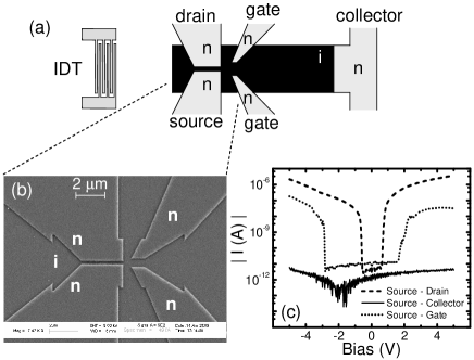
The device was fabricated starting from a n-type modulation-doped Al0.3Ga0.7As/GaAs heterostructure grown by molecular-beam epitaxy, containing a two dimensional electron gas (2DEG) within a 30-nm-wide GaAs quantum well embedded 90 nm below the surface. The measured electron density and mobility after illumination at 1.5 K were cm-2 and cm2/Vs, respectively. The heterostructure was processed into mesas with annealed n-type Ni/AuGe/Ni/Au (10/180/10/100 nm) Ohmic contacts by standard optical lithography, wet chemical etching and thermal evaporation. The n-i-n lateral-junction was fabricated according to the scheme of Fig. 1 (a). Two portions of the 2DEG (named “source” and “drain”) were separated by a thin intrinsic spacer (which we shall call “the barrier” in the following) defined by electron beam lithography and shallow ( nm) etching of the surface. We observed that a 30-nm etching leads to QW depletion allowing to create intrinsic regions within the mesa. A 70-m long intrinsic region (“the channel” in the following) defined by the same etching step described above separates the n-i-n region from a third electron reservoir (the “collector”.)
A pair of lateral control gates consisting of portions of 2DEG were also fabricated to allow further control on the collector current Gloos et al. (2004). Figure 1 (b) displays a scanning electron microscope image of the injector and gate region.
The source-drain separation was chosen of 250 nm in order to have a breakdown voltage of approximately 1 V. Figure 1(c) shows the low temperature ( K) current-voltage characteristics between the different n-regions (source, drain and collector) after illumination. We observed a conduction threshold between source and drain contacts of V, while the source-gate conduction threshold was found to be much higher, owing to the larger distance between these electrodes. As expected, is negligible within the explored range of voltages. The observed asymmetry of the I-V curves shown in Fig. 1(c) does not affect the device operation and was probably due to device inhomogeneities introduced during the wet etching process.
SAWs propagating along the (01̄1̄) crystal direction were generated by means of an interdigital transducer (IDT) composed of 100 pairs of 80-m-long Al fingers with 1-m periodicity ( GHz resonance frequency on GaAs). Transducers were fabricated at a distance of 500 m from the n-i-n injector by electron-beam lithography. The IDT resonance frequency was determined by measuring the power reflected by the IDT as a function of the excitation frequency. The low temperature ( K) frequency response displayed a dip at 2.929 GHz with a full width at half maximum (FWHM) of 2 MHz, consistently with the periodicity of the transducer.
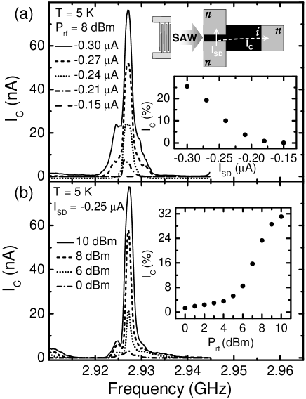
We monitored by means of a low-noise current preamplifier in the presence of SAWs while injecting a constant source-drain current, . The gates were left floating and the temperature was set at K. Figure 2 (a) shows as a function of the frequency of the signal applied to the IDT for from -0.15 A to -0.30 A.
A pronounced current peak, corresponding to electrons getting to the collector through the intrinsic region, was detected at the SAW excitation frequency for A. The height of the peak increases by making more negative. The electron extraction efficiency, defined as the fraction of detected at the collector, also increases [see the inset of Fig. 2 (a)], reaching the value of for A.
To study the SAW extraction efficiency, was measured as a function of the frequency of the IDT excitation signal at fixed at different SAW power levels. We observed ACT for dBm, where is the power of the signal applied to the transducer. The electron extraction efficiency increases with , reaching approximately the value of at dBm.
Qualitatively analogue behavior was obtained by fixing the n-i-n injector voltage, , instead of the current, demonstrating the possibility to process both voltage and current signals.
By inverting the sign of , i. e. by biasing one lead of the n-i-n injector with positive voltage with respect to the ground and maintaining the other lead grounded, no ACT was observed. Indeed, this corresponds to lowering the conduction band bottom of the barrier with respect to the channel. In this regime the SAW potential is not able to drive electrons from the barrier to the channel.
All the measurements described above were carried out from K up to room temperature. The behavior of the device was essentially determined by the change of the conduction threshold of the injector junction. This indeed progressively increased up to unacceptable values ( V) for T 120 K. Low conduction threshold was recovered by further increasing the temperature, but no ACT was observed in this high temperature regime.
Finally, we analyzed the effect of the lateral gates on ACT. By applying negative voltages to the gates we expect that the channel available for electron transfer to the collector become progressively narrower and eventually pinches off. The acoustoelectric current toward the OC is thus expected to decrease and eventually vanish at sufficiently large negative voltage. Figure 3 demonstrates the modulation of the ACT by means of in-plane lateral gates. The collector current was measured as a function of the frequency of the signal applied to the IDT for several values of the gate voltage111Both gates were always biased at the same voltage. and for a fixed injector current (or bias). The resonance peak was observed to decrease for gate voltages more negative than -0.5 V. As shown in the inset of Fig. 3, this effect saturates at V. Within this range of voltage the peak current was reduced by . We could not completely suppress ACT because more negative gate voltages led to current leakage toward the n-electrodes of the injector. Optimization of the gate-injector geometry can prevent current leakage and allow the use of the gates over a wider range of voltage.
In conclusion, we demonstrated ACT in an original device consisting in a lateral n-i-n injector junction, an etched intrinsic channel, an output ohmic contact and a pair of in-plane gates. We showed that SAWs can extract electrons from a current flowing through the n-i-n injector and transport them toward the output contact. ACT was fully characterized as a function of the injector current and bias, the SAW power and at various temperature from 5 K to room temperature. Finally, we demonstrated the possibility to modulate the acoustoelectric current by means of lateral in-plane gates.
This work was supported in part by the European Commission through the IP SECOQC within FP6 and by MIUR within FISR Nanodispositivi ottici a pochi fotoni.
References
- Hoskins et al. (1982) M. J. Hoskins, H. Morkoç, and B. J. Hunsinger, Appl. Phys. Lett. 41, 332 (1982).
- Guediri et al. (1987) F. Guediri, R. L. Martin, B. J. Hunsinger, and F. M. Fliegel, Proc. IEEE Ultrasonic Symp. p. 11 (1987).
- Edjeou et al. (2000) T. Edjeou, T. Gryba, V. Zhang, V. Sadaune, and J. E. Lefebvre, Solid State Electron. 44, 1127 (2000).
- Esslinger et al. (1994) A. Esslinger, R. W. Winkler, C. Rocke, A. Wixforth, J. P. Kotthaus, H. Nickel, W. Schlapp, and R. L sch, Surf. Sci. 305, 83 (1994).
- Esslinger et al. (1992) A. Esslinger, A. Wixforth, R. W. Winkler, J. P. Kotthaus, H. Nickel, W. Schlapp, and R. L sch, Solid State Commun. 84, 939 (1992).
- Campbell et al. (1992) J. W. M. Campbell, F. Guillon, M. D’Iorio, M. Buchanan, and R. J. Stoner, Solid State Commun. 84, 735 (1992).
- Miller et al. (1992) R. L. Miller, C. E. Nothnick, and D. S. Bailey, Acoustic charge transport: device technology and applications (Artech House, 1992).
- Ratolojanahary et al. (2004) F. E. Ratolojanahary, T. Gryba, and F. L. Razafindramisa, IEE P-Circ. Dev. Syst. 151, 322 (2004).
- Gloos et al. (2004) K. Gloos, P. Utko, J. B. Hansen, and P. E. Lindelof, Phys. Rev. B 70, 235345 (2004).