Competing periodicities in fractionally filled one-dimensional bands
Abstract
We present a variable temperature Scanning Tunneling Microscopy and Spectroscopy (STM and STS) study of the Si(553)-Au atomic chain reconstruction. This quasi one-dimensional (1D) system undergoes at least two charge density wave (CDW) transitions at low temperature, which can be attributed to electronic instabilities in the fractionally-filled 1D bands of the high-symmetry phase. Upon cooling, Si(553)-Au first undergoes a single-band Peierls distortion, resulting in period doubling along the imaged chains. This Peierls state is ultimately overcome by a competing triple-period CDW, which in turn is accompanied by a periodicity in between the chains. These locked-in periodicities indicate small charge transfer between the nearly half-filled and quarter-filled 1D bands. The presence and the mobility of atomic scale dislocations in the CDW state indicates the possibility of manipulating phase solitons carrying a (spin,charge) of () or ().
pacs:
73.20.At, 73.20.Mf, 71.10.Pm, 68.37.EfAccording to the Mermin-Wagner theorem Mermin66-68 , thermodynamic fluctuations preclude the formation of a long-range ordered broken symmetry state in 1D, except at T = 0 K Rice73Pytte74 . For all practical purposes, however, thermodynamic phase transitions may still be possible in finite size 1D systems. Furthermore, fluctuations are inevitably suppressed if the 1D chains are weakly coupled, or if the chains are coupled to a substrate Rice73Pytte74 ; Lee04Shannon96 . Prototypical 1D metallic systems like the transition metal trichalcogenides, organic charge transfer salts, blue bronzes, and probably all atomic Au-chain reconstructions on vicinal Si substrates exhibit symmetry breaking phase transitions at finite temperatures Gruner85 ; Yeom05 . For a band filling of , the phase transition opens up a gap in the single particle excitation spectrum at wavevector , and the corresponding broken symmetry state adopts the new periodicity of , where is the lattice parameter of the high symmetry phase Gruner85 .
Fractional band fillings other than half filling provide an interesting subset of 1D systems which often exhibit exotic physical phenomena. Depending on the relative magnitude of bandwidth and electron-electron interaction, CDW states often compete with spin density waves, Mott insulating states, or a Luttinger liquid state. Atomic-scale STM observations of surface phase transitions provide important insights into the complexity of symmetry breaking phenomena in reduced dimensionality In . For instance, the recently reported -to- phase transition in quasi-1D indium chains on Si(111) In involves a gap opening in a complex triple band Peierls system, resulting in a doubling of the periodicity along the atom chains. Another recently discovered system with three fractionally-filled bands is the Si(553)-Au surface. Angle-resolved photoemission spectroscopy (ARPES) Crain0304 revealed three metallic bands but despite theoretical efforts to understand the electronic structure Riikonen05 ; Crain0304 the atomic structure and real space location of the surface state orbitals remains unknown. Interestingly, the total band filling of this particular chain system is , i.e. corresponding to electrons per surface unit cell. Two bands have a filling of 0.56 and 0.51 each, slightly more than half-filling. The third band has a filling of 0.27, in between one quarter and one-third filling.
In this Letter we present evidence for a defect mediated CDW transition Hanno99 in Si(553)-Au accompanied by a metal insulator transition. STM experiments reveal competing periodicities as a function of temperature which can be mapped onto the band structure of the high symmetry phase. STS data show a gradual gap opening at low temperatures, which can be correlated with successive gap openings in the three 1D bands. Interestingly, phase slips are observed in the CDW condensate. These phase slips should possess a fractional charge and a half integer or integer spin. The chain-length can be tuned by manipulating the numerous defects with the STM tip. This, in turn, suggests the feasibility of studying and manipulating fractional charges at the atomic scale.
The Si(553)-Au structure was prepared by depositing 0.24 ML of Au at a rate of 0.005 ML/s with the substrate held at 920 K, followed by thermal annealing at 1120 K for 1 minute and slow cooling to room temperature or RT (1 K). STM and STS experiments were performed in an Omicron variable temperature STM. All distances determined in STM images were measured along the fast scan direction of the STM so as to minimize possible effects of thermal drift.
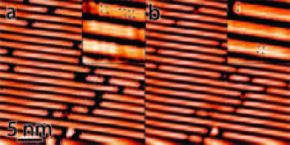
Figure 1 shows an STM image of the surface taken at room temperature (RT). Rather wide chains ( nm) with a spacing of 1.48 nm are observed. The chains are cut by point defects appearing as vacancies in both filled state and empty state images. In the empty state image, these vacancies appear larger than in the filled state image, confirming the observations reported in Ref. Crain05, . Note, however, that fewer defects are present as compared to other work Crain0304 ; Crain05 , indicating that the defect concentration can possibly be varied by controlling the annealing history of the surface despite propositions that the defects might be intrinsic to the surface as stabilizing charge dopants Crain0304 . The insets show high resolution dual bias images. Clearly, the chains are composed of two rows of atoms, showing a zig-zag structure in the empty state and a ladder configuration in the filled state. In the empty state image all atom spacings are nearly equal to the bulk spacing of Si, Å resulting in bond angles near 60 degrees. In the filled state image the spacing along the chain is equal to whereas the spacing perpendicular to the chains is Å. These data seem to be inconsistent with structure models that place Si honeycomb chains Hanno98 near the step edges Crain0304 ; Riikonen05 and with the single atom row structure suggested in Ref. Crain05, .
Upon cooling to K, the zig-zag features are no longer observed. Instead, an up-down buckling with a ladder structure in a tripled unit cell is observed (Fig. 2), resulting in two features of about length and widths comparable to those observed at RT. The corrugation of the filled state image is in anti-phase with that of the empty state image; at the location of the intensity maxima in the empty state image, a small dip exists in the filled state image. This indicates that the system has condensed into a CDW with tripled periodicity, commensurate with the substrate lattice. Additionally, the features in the valleys between the chains visible in the empty state are completely ordered with a doubled period of , resulting in a unit cell of .
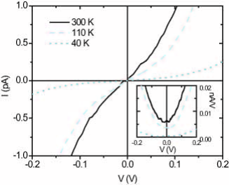
The -curves and their numerical derivatives are shown in Fig. 3. The -curve at RT exhibits a significant slope at zero bias, confirming the metallicity observed in ARPES experiments Crain0304 . In contrast, at 40 K the -curve is flat at zero bias indicating semiconducting behavior. We determine the size of the gap from the derivative of the -curves as displayed in the inset of Fig. 3; we infer that the excitation gap is symmetric and meV wide. Thus, the condensation of this CDW is accompanied by a metal-insulator transition (MIT). Although CDW instabilities in related surface systems are often manifested by an order-disorder transition Avila99 , the present observations are most straightforwardly interpreted in terms of a displacive CDW transition.
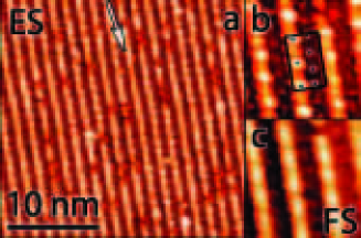
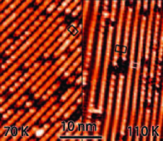
The condensation scenario involving all three 1D bands is elucidated by STM experiments at temperatures intermediate between RT and 40 K. Fig. 4 shows empty state images measured at 70 K and at 110 K. At 70 K a vague tripled corrugation is visible in nearly all of the chains, with significantly enhanced intensity near defects. In the middle of longer chains segments the bulk period of Å is still visible through the superimposed (vague) tripled periodicity. At 110 K, we observe a doubled periodicity in the bulk of most chains, but, again near defects a tripled periodicity decaying into the chains is observed. From these data at higher temperatures, it is evident that the CDW present at 40 K nucleates from the defects and spreads along the chains with decreasing temperature. Even at RT, it is still possible to discern charge density oscillations emanating from the defects. These oscillations have been attributed to zero-dimensional end state effects Crain05 . Alternatively, the change in apparent height of the chain adjacent to a defect, i.e. a depression over a distance of next to the defect followed by a brighter segment (see Fig. 1(a):inset), and the non-metallic character of the chain ends established in Ref. Crain05 , are fully consistent with the interpretation of a CDW precursor, similar to that observed in Sn/Ge(111) Hanno99 .
As mentioned above, the band structure of this surface measured by ARPES contains three metallic bands Crain0304 ; two bands have a Fermi wave vector near half-filling, the third band contains electrons adding up to a total filling of . None of the bands crosses the Fermi energy exactly at a wave vector . Nevertheless, we observe three commensurate periodicities evolving as a function of temperature: at 110 K a clear period is detected in the chains, at 40 K a period is observed between the chains accompanied by a period in the chains. Tentatively, we assign the three observed periods to electronic instabilities in the three metallic bands of the high symmetry phase, which would locate the orbitals of the 0.51 and 0.27 filled bands on top of the zig-zag chains and the orbitals of the 0.56 filled band in between the chains. At 110 K, the doubled periodicity along the chains originates from a CDW transition in the 0.51 filled band; the other two bands remain metallic. STS measurements support this scenario, still showing metallic behaviour at 110 K but with reduced slope at zero bias, indicating a reduced DOS at the Fermi energy, see Fig. 3. ARPES at temperatures K show weak backfolding of the 0.27 filled band at the zone boundary Crain0304 , also indicating a doubled periodicity in this band. The CDW at lower temperatures can then be rationalized by a small charge transfer of 0.06 electron from the 0.56 filled band to the 0.27 filled band, filling the latter to 11endnote: 1According to Ref. Schrieffer73 , a commensurate CDW in a system with incommensurate Fermi wave-vectors can be obtained by locking the wavelength of the CDW to the lattice so as to be commensurate. However, then it would be expected that the 0.27 filled band would lock to a period corresponding to a filling of 0.25.. The possible CDW precursor near the chain ends at RT can also be explained by this charge transfer: at RT a period exists locally in between the chains near defects that are located on the chains Crain05 . This strongly suggests that already at RT the 0.56 filled band, located in the valleys between the chains, is doping the chains near the defects to filling. With this charge transfer the total band filling of the surface then remains constant at . Note that this evolution in band structure might also explain the transformation of the features in the empty state STM image; from a zig-zag structure at RT to a ladder structure at 110 K and below.
Surprisingly, the competition between periodicities inside the chains is eventually won by a CDW at the lowest temperature studied. Longer wavelength periods are progressively more difficult to fit into chains with randomly placed fixed defects. Furthermore, a filled parabolic band has a higher DOS at the Fermi energy as compared to a filled band, which according to a simple BCS theory argument should result in a higher for the filled band. The magnitude of the interchain coupling for the different bands, though being fairly low as compared to other (bulk) 1D compounds Crain0304 , might provide insight into this seeming contradiction. It is well known that finite interchain coupling reduces the transition temperature and indeed ARPES measurements indicate a five times larger interchain coupling for the filled band than for both of the filled bands. This could explain why the CDW sets in at a lower temperature than the period doubling CDW observed at 110 K 22endnote: 2An alternative explanation is that the relatively large charge transfer into the 0.27 filled band induces significant more lattice strain, thereby lowering its Tc as compared to the CDW..
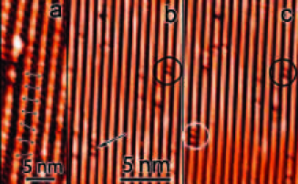
Finite interchain coupling should be discernible in the STM images through definite phase relations between periodicities in adjacent chains, provided that the temperature is low enough. Careful analysis of the empty state STM images at 40 K indeed reveals small domains of up to three or four chains width, showing a constant phase relation, but no long range order is detected. However, as can be observed in Fig. 2(a, arrow) even at 40 K there are chains which do not exhibit a fully developed CDW; the triple periodicity is not long range ordered, despite the fact that a fully developed triple period would fit the length of this chain segment. This indicates that the system is affected by a significant amount of interchain coupling. This is further illustrated in Fig. 5(a). Two fairly long chains ( nm) are visible. Starting from the top both chains lack a clear corrugation, but both chains develop a definite up-down corrugation towards the bottom. The white bars illustrate a phase slip of in the right chain, immediately followed by two similar phase slips in the left chain. These phase slips can not be explained by a CDW mismatch in a finite chain segment because both chains show a region of small corrugation at the top (and beyond, not shown) with an ill-defined phase so the CDW is not phase locked by defects. Therefore the origin must be related to interchain coupling; apparently, a phase slip in one chain can induce phase slips in neighboring chains via interchain coupling. Interestingly, a phase slip (phase soliton) in a filled band CDW carries a (spin,charge) of () or () Su81Kuhn95 .
Fractionally charged phase slips have been studied mostly theoretically. Only in polyacetylene, a phase slip with a fractional charge of has been observed by conductivity and NMR experiments Su80 . To the best of our knowledge fractionally charged phase slips in CDWs away from half filling have never been observed directly by imaging. Their presence opens up the possibility to study and manipulate fractional charges at the atomic scale. They can possibly be manipulated by deliberately creating defects in the chains so as to generate a misfit for the CDW. In our STM experiments at 40 K defects sometimes jump to different locations during imaging. For example, Figs. 5(b) and (c) show two sequential () filled state images from the same area. The white circle and the arrow show a group of three defects which has moved two chains to the left. This behavior suggests that these defects consist of Si adatoms Crain0304 ; Riikonen05 , which have been relocated by tip induced migration.
In conclusion, we have presented an STM and STS study of a chain structure with fractional band fillings. Competing periodicities are observed as a function of temperature resulting in a defect mediated CDW at 40 K. The results can be mapped onto the band structure of the high symmetry phase. The presence and mobility of the chain dislocations in the CDW state indicates the possibility of studying and possibly manipulating fractionally charged solitons with an STM tip. The availability of other vicinal Si-Au chain structures with tunable interchain coupling Crain0304 would provide a promising playground for 1D physics, accessible in real space. Note added: After the submission of our manuscript, we became aware of the paper by Ahn et al. Ahn05 . Their observations are consistent with ours.
We thank Prof. Franz Himpsel for providing the Si(553) wafer. This work is sponsored in part by NSF under contract No. DMR-0244570, the Stichting voor Fundamenteel Onderzoek der Materie and the Royal Netherlands Academy of Arts and Sciences. We thank T.M. Klapwijk for his stimulating support. Oak Ridge National Laboratory is managed by UT-Battelle, LLC, for the US Department of Energy under contract No. DE-AC-05-00OR22725.
References
- (1) N.D. Mermin, H. Wagner, Phys. Rev. Lett. 17, 1133 (1966), N.D. Mermin, Phys. Rev. 176, 250 (1968).
- (2) M.J. Rice, S. Strässler, Solid State Commun. 13, 1389 (1973), E. Pytte, Phys. Rev. B 10, 2039 (1974).
- (3) M. Lee, E.A. Kim, J.S. Lim, M.Y. Choi, Phys. Rev. B 69, 115117 (2004), N. Shannon, R. Joynt, J. Phys.: Condens. Matter 8, 10493 (1996).
- (4) G. Grüner, A. Zettl, Physics Reports 119, 117 (1985).
- (5) H.W. Yeom et al., Phys. Rev. B 72, 035323 (2005).
- (6) H.W. Yeom, K. Horikoshi, H.M. Zhang, K. Ono, R.I.G. Uhrberg, Phys. Rev. B 65, 241307(R) (2002), S.J. Park, H.W. Yeom, S.H. Min, D.H. Park, I.W. Lyo, Phys. Rev. Lett. 93, 106402 (2004), G. Lee, J. Guo, E.W. Plummer, Phys. Rev. Lett. 95, 116103 (2005), H. Morikawa, I. Matsuda, S. Hasegawa, Phys. Rev. B 70, 085412 (2004), J. Guo, G. Lee, E.W. Plummer, Phys Rev. Lett. 95, 046102 (2005).
- (7) J.N. Crain et al., Phys. Rev. Lett. 90, 176805 (2003), J.N. Crain et al., Phys. Rev. B. 69, 125401 (2004).
- (8) S. Riikonen, D. Sanchez-Portal, Nanotechnology 16, S218 (2005).
- (9) H.H. Weitering et al., Science 285, 2107 (1999).
- (10) J.N. Crain, D.T. Pierce, Science 307, 703 (2005).
- (11) S.C. Erwin, H.H. Weitering, Phys. Rev. Lett. 81, 2296 (1998).
- (12) J. Avila et al., Phys. Rev. Lett. 82, 442 (1999).
- (13) J.R. Schrieffer, Nobel Symposium 24 (Academic, New York and London, 1973), p. 142.
- (14) W.P. Su, J.R. Schrieffer, Phys. Rev. Lett. 46, 738 (1981), C. Kuhn, J. Phys. Condens. Matt. 7, 6221 (1995).
- (15) W.P. Su, J.R. Schrieffer, A.J Heeger, Phys. Rev. B 22, 2099 (1980).
- (16) J.R. Ahn et al., Phys. Rev. Lett. 95, 196402 (2005)