Scanning tunneling microscopy of surfaces of half-metals: an ab-initio study on NiMnSb(001)
Abstract
We present a first-principles study of the unreconstructed (001) surfaces of the half-metallic ferromagnet NiMnSb. Both terminations (MnSb and Ni) are considered. We find that half-metallicity is lost at the surfaces. After a discussion of the geometric relaxations and the spin-polarized surface band structure, we focus on topography images which are expected to be found with spin-polarized scanning tunneling microscopy. For the MnSb-terminated surface we find that only the Sb atoms are visible, reflecting a geometric buckling caused by relaxations. For the Ni-terminated surface we find a strong contrast between the images of forward and reverse tip-sample-bias of 0.5 eV, as well as a stripe-like image for reverse bias. We interpret these findings in terms of highly directional surface states which are formed in the spin-down gap region.
pacs:
73.20.At,71.20.Lp,75.70.Rf1 Introduction
Half-metallic Heusler alloys have attracted considerable attention lately, because of their potential applications to spintronics. In particular, the desirable half-metallic character (100% spin polarization at the Fermi level ), which renders them candidates for efficient spin-dependent transport, has been predicted by numerous calculations for many half- and full-Heusler alloys [1, 2, 3, 4]. The surfaces of Heusler alloys have also been examined, in the hope of probing the half-metallic property there. It seems, though, that the spin polarization is strongly reduced, or even reversed, at surfaces, and that the half-metallic gap is lost: computational results [5, 6, 7, 8] suggest that this is due to surface states which are formed by broken bonds; spin-polarized photoemission spectroscopy does also not show half-metallicity at the surfaces [9].
In a previous study [8] we presented first-principles calculations on the NiMnSb(001) and (111) surfaces, showing how the surface states appear within the gap and close it. We also described in detail how these states can develop to interface states [10] and how these interface states affect the spin-dependent transport properties, in particular when half-metals are used as leads in tunnel junctions [11]. In this paper we extend our work to the study of spin-dependent scanning tunneling microscopy (SP-STM) images of the NiMnSb(001) surfaces. Our focus is on the possibility to distinguish the two possible (001) terminations (Ni and MnSb), and on the form of the topography pictures for charge density, magnetization density, and spin-resolved density.
2 Method of calculation
The calculations were performed within the generalized gradient approximation (GGA) [12] of density functional theory. We used the full-potential linearized augmented planewave (FLAPW) method in film geometry [13], as implemented in the FLEUR code [14]. For the calculations, a planewave cutoff of 3.6 a.u.-1 was used. The charge density and the wavefunctions within the muffin-tin spheres ( Å ; Å) were expanded in lattice harmonics with angular momentum . We modeled the (001) surfaces using a slab of 9 atomic layers of NiMnSb. The two-dimensional Brillouin zone was sampled with 64 special k-points in the irreducible wedge. All the calculations were performed at the theoretically determined equilibrium in-plane lattice constant of NiMnSb (5.915 Å), which is within 0.2% in agreement with the experimental value [15]. The atomic structure was optimized by calculation of the forces on the three topmost layers of the film. Possible reconstructions were not considered.
3 Results and discussion
3.1 Unrelaxed and relaxed surface structure
NiMnSb crystallizes in the L21 structure, consisting of three inter-penetrating fcc sublattices. Viewed as a succession of atomic planes in the direction, the structure consists of alternating Ni and MnSb layers, with the layer occupancy and geometry repeating every fourth layer. The interlayer distance is /4 (with being the bulk lattice constant). Thus, chemically, the (001) surface has two different possible terminations: one with Mn and Sb at the surface, and one with Ni (see Figure 1). Geometrically, the layer occupancy is repeated every fourth layer, since every second layer the atoms exchange positions (Mn with Sb and Ni with the empty site; thus the top view of every second layer is equivalent but rotated by ). The surface symmetry group is . On the question of surface reconstruction, we point out that Ristoiu and collaborators [16] found an unreconstructed surface by low energy electron diffraction experiments, and that Jenkins and King [5] report that the unreconstructed MnSb-terminated surface is energetically lower than the reconstructed one.
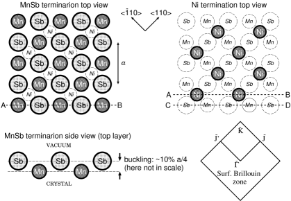
In the calculations for the structural relaxation of the surfaces we allowed in each case for the three top layers to relax. For the Ni terminated surface we find that the distance to the subsurface layer is reduced by 10%, while there is no appreciable buckling or relaxation of the subsurface MnSb layer. In the case of the MnSb terminated surface, we find that for the Sb atoms is expanded by 7.3%, while for the Mn atoms is contracted by 3.5%. This gives an overall buckling of 10.8% of the interlayer distance . This is in reasonable agreement with the buckling determined by Jenkins and King [5], and, as we see below, is important for the STM images of the MnSb-terminated surface.
3.2 Surface electronic and magnetic structure
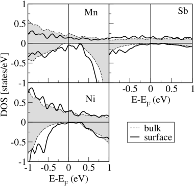
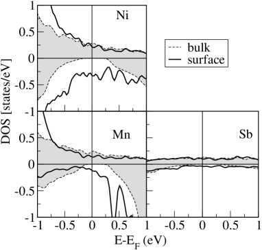
The densities of states (DOS) of the NiMnSb(001) surface and sub-surface layers close to the Fermi level are shown in Figure 2 together with the bulk DOS for comparison. Clearly, the spin-down gap which is present in the bulk closes at the surface. The surface states responsible for this loss of half-metallicity come about due to the broken translational symmetry at the surface. As pointed out in reference [3], the spin-down gap at originates from the hybridization of the Mn orbitals with the Ni orbitals. Since this hybridization ceases at the surface, the gap collapses. For a detailed study on the origin and nature of these surface states we refer to the works of Jenkins and King [5] and Ležaić et al. [8]. We will discuss them further in connection to the STM images in the next subsection.
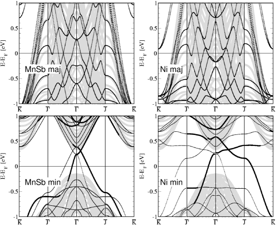
The surface band structure of NiMnSb(001) is presented in Figure 3. Because the calculation involves a finite slab, the surface bands come in pairs, one band for each slab surface. We identify the bands of a single surface as those with more than 50% weight within the first two surface layers; this results in the thickly marked bands of Figure 3.
3.3 STM images
For the STM topography images we use the model of Tersoff and Hamann [17], according to which the tunneling current from or into the tip above a lateral surface point and at a vertical distance from the surface at a bias voltage is proportional to the integrated density of states at the position of the tip,
| (1) |
for (and the same but integrated from to for ), with being the local DOS of the sample at the position of the tip apex. We chose eV and vertical distances of Å and 4 Å (taken from the muffin-tin boundary of the surface atoms; see section 2). Our results, showing the integrated DOS, were qualitatively the same for both distances, and below we show the images calculated for Å from the surface layer.
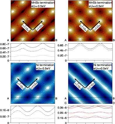
The STM topography for the MnSb-terminated surface is shown in Figure 4 (upper panels). The first striking effect is that only the Sb atoms are visible, while above the Mn atoms the tunneling current shows local minima. This is mainly caused by the aforementioned 10.8% buckling of the surface atoms, which renders the retracted Mn atoms invisible to the STM tip. Thus, it is not possible to distinguish the MnSb-termination by its higher atomic density compared to the Ni-termination: the extra atoms are “hidden”.
Nevertheless, a second striking effect is revealed when one compares the topography for both signs of the voltage . While for the MnSb termination is comparable in magnitude for both bias voltages eV, for the Ni termination there is a difference between and of a factor three (the corrugation, however, is of the same magnitude). This is demonstrated in Figure 4 (bottom panels), where we have plotted line scans of along the direction. At the same time, the topographic image at eV shows stripes in the direction, with the positions of the atoms barely visible, together with a corrugation in the direction. The image at eV, on the contrary, shows comparatively little directionality, with more symmetric patterns around the Ni atoms.
Given this effect, the nature of the surface can be readily found in an STM experiment by the strong contrast between forward- and reverse-bias currents and images at the Ni-terminated surface, as opposed to the comparable forward- and reverse-bias currents at the MnSb-termination.
In order to explain this contrast, we observe that, for the Ni-termination, surface states appear in the direction between 0.1 eV and 0.5 eV above (see Figure 3). At this point we recall that most of the tunneling current results from states around the -point, but the topography images (the corrugation) are frequently determined by states in the vicinity of high-symmetry points at the Brillouin zone boundary [18]. This is consistent with the observation that the directionality of the surface states in -space is reflected in the stripy topographic pattern; the corrugation is in the direction, as a result of the states close to the surface Brillouin zone boundary . From the line scan (Figure 4) it is also evident that the main contribution to the STM intensity comes from spin-down electrons. The corrugation, however, comes from both spin directions in an alternating pattern, as can be seen from the difference between the line scans along AB and CD. The former one (AB) passes over the atoms, where the spin-up states contribute to the expected corrugation. The latter line scan (CD) passes over the interatomic bridge positions, where the spin-down orbitals, showing a directional preference, form those one-dimensional surface states which are dispersive along the direction (represented by in Figure 3) and non-dispersive along the direction (represented by in Figure 3).
We interpret the dispersive form of these surface bands as follows. Due to the subsurface atoms, the (001) surface has only a twofold symmetry with natural coordinate axes along the direction (we call this the axis) and along the direction (we call this the axis). Then the orbitals at the surface have an overlap along the axis, resulting in dispersive bands, but no overlap along the axis, resulting in non-dispersive bands. Therefore in the spin-down surface band structure of the Ni-terminated surface (Figure 3) we see, at the -point and at about 0.2 eV, one dispersive band departing towards the direction and one non-dispersive band departing towards the direction. The overlap of the orbitals is mediated by - hybridization with the underlying Mn atoms. On the contrary, the orbitals are oriented towards the underlying Sb atoms, so that a corresponding hybridization cannot take place (the states are orthogonal to the states of the Sb neighbors). Therefore, we obtain the second band at , at 0.5 eV, which is non-dispersive in both directions. (For a discussion of one-dimensional surface states in the MnSb-terminated surface, see reference [5].)
In order to cross-check our explanation on the origin of the striped pattern, we produced topographic images for bias voltages of V. We expect that the striped pattern and the high spin-down DOS will disappear for the image of eV, since the narrow spin-down surface states are present only above eV. The images (not shown here) verify our hypothesis, showing now fourfold symmetry, with the density dominated by spin-up states; furthermore the intensity for eV appears twice as strong as for eV, i.e., the situation is reversed compared to the 0.5 V case.
In view of the above results we conclude that STM topography can distinguish the Ni-terminated from the MnSb-terminated (001) surface by the contrast between forward- and reverse-bias images at 0.5 V, as well as by the striped, corrugated pattern which appears for eV.
We conclude the discussion with a comment on spin-polarized STM images for the Ni-terminated surface at eV. From the line scans it is evident that the spin-up and spin-down corrugations are complementary. This means that, in an ideal SP-STM experiment the spin-up contrast will be stronger above the atoms (in accordance with general wisdom for STM on metallic surfaces), while the spin-down contrast will be stronger above the bridge positions (contrary to general wisdom). The stripy features will disappear. We verified this by plotting the corresponding two-dimensional STM images (not shown here). In a real SP-STM experiment, of course, the difference between the two spins will be captured to the extent of the spin-filtering quality of the spin-polarized tip.
4 Summary and outlook
We have investigated the NiMnSb(001) unreconstructed surfaces by first-principles calculations. Emphasis was given on the STM topographic images and their relation to the surface geometry and electronic structure.
There are two possible terminations: a MnSb termination and a Ni termination. In both cases we find that half-metallicity, which is present in the bulk, is lost at the surface. This is attributed to the breaking of - hybridization bonds (between the Mn and Ni states) which are actually responsible for the gap in the bulk. The surface states which are thus formed are mainly of character.
For the MnSb-terminated surface, relaxation of the atomic positions results in a buckling of about 10.8% with respect to the interlayer distance, with the Sb atoms protruding outwards. This buckling is significant for the STM image, because it renders the Mn atoms invisible to the STM tip. From previous work [5] on the MnSb surface, surface reconstruction is not expected.
For the Ni-terminated surface the STM images at eV show a peculiar stripe-like corrugation. This partly originates from spin-up states, which give a contrast above the Ni atoms, and partly from the spin-down states, which give a contrast above the bridge positions. The latter effect can be traced back to the form of the spin-down -like surface bands. In particular, the surface has twofold symmetry, which is inherited by the surface band structure because of the bonding via the underlying Mn atoms. As a result, the spin-down surface states are dispersive in the direction and non-dispersive in . In addition, we find that the current is dominated by spin-down states. These features disappear at bias voltages lower than eV, which corresponds to the bottom of the narrow spin-down surface bands; below this voltage, the spin-down current and corrugation become unimportant.
As an outlook, we comment on the possibility of spin-polarized STM in the case that a surface would be half-metallic. Such surfaces have been predicted to exist in some half-metallic systems, including transition-metal pnictides and chalcogenides in the zinc-blende structure [19] or even the Mn-rich, Mn-terminated Co2MnSi(001) surface [20]. In such cases no spin-down current should exist. However, since the tip itself is normally not half-metallic, the spin-up (with respect to the sample) current is present for both orientations of the tip magnetization (parallel and antiparallel to the sample). Thus one should expect a strong asymmetry by reversing the tip magnetization, but not an effect of absolute current blockade. Additionally, there should be a drastic increase of the current when the increased bias reaches the valence band or the conduction band of the spin-down channel.
Acknowledgements
We would like to thank Stefan Heinze for a critical reading of the manuscript.
References
References
- [1] de Groot R A, Mueller F M, van Engen P G and Buschow K H J 1983 Phys. Rev. Lett.50 2024
- [2] For a recent review on Heusler alloys see Galanakis I and Dederichs P H (eds): Half-metallic alloys: fundamentals and applications, Springer Lecture notes in Physics vol. 676, Springer (2005).
- [3] Galanakis I, Dederichs P H and Papanikolaou N 2002 Phys. Rev.B 66 134428
- [4] Picozzi S, Continenza A and Freeman A J 2002 Phys. Rev.B 66 094421; Galanakis I, Papanikolaou N and Dederichs P H 2002 Phys. Rev.B 66 174429
- [5] Jenkins S J and King D A 2001 Surf. Sci. 494 L793
- [6] Galanakis I 2002 J. Phys.: Condens. Matter14 6329
- [7] Jenkins S J 2004 Phys. Rev.B 70 245401
- [8] Ležaić M, Galanakis I, Bihlmayer G, and Blügel S 2005 J. Phys.: Condens. Matter17 3121
- [9] Bona, G L; Meier, F; Taborelli, M; Bucher, E; Schmidt, P H 1985 Solid State Commun. 56, 391 Zhu W, Sinkovic B, Vescovo E, Tanaka C and Moodera J S 2001 Phys. Rev.B 64 060403(R)
- [10] Galanakis I, Ležaić M, Bihlmayer G and Blügel S 2005 Phys. Rev.B 71, 214431
- [11] Mavropoulos Ph, Ležaić M, and Blügel S 2005 preprint: cond-mat/0506079
- [12] Perdew J P, Burke K and Ernzerhof M 1996 Phys. Rev. Lett.77 3865
- [13] Wimmer E, Krakauer H, Weinert M and Freeman A J 1981 Phys. Rev.B 24 864; Weinert M, Wimmer E and Freeman A J 1982 Phys. Rev.B 26 4571
- [14] http://www.flapw.de
- [15] Otto M J, van Woerden R A M, van der Valk P J, Wijngaard J, van Bruggen C F, Haas C and Buschow K H J 1989 J. Phys.: Condens. Matter1 2341
- [16] Ristoiu D, Nozières J P, Borca C N, Komesu T, Jeong H -K and Dowben P A 2000 Europhys. Lett. 49 624
- [17] Tersoff J and Hamann D R 1983 Phys. Rev. Lett.50, 1998
- [18] Heinze S, Blügel S, Pascal R, Bode M, and Wiesendanger R 1998 Phys. Rev.B 58, 16432
- [19] Galanakis I 2002 Phys. Rev.B 66 012406; Galanakis I and Mavropoulos Ph 2003 Phys. Rev.B 67 104417
- [20] Javad Hashemifar S, Kratzer P, and Scheffler M 2005 Phys. Rev. Lett.94, 096402