The role of Joule heating in the formation of nanogaps by electromigration
Abstract
We investigate the formation of nanogaps in gold wires due to electromigration. We show that the breaking process will not start until a local temperature of typically 400 K is reached by Joule heating. This value is rather independent of the temperature of the sample environment (4.2-295 K). Furthermore, we demonstrate that the breaking dynamics can be controlled by minimizing the total series resistance of the system. In this way, the local temperature rise just before break down is limited and melting effects are prevented. Hence, electrodes with gaps 2 nm are easily made, without the need of active feedback. For optimized samples, we observe quantized conductance steps prior the gap formation.
I introduction
For single molecular electronics, electrodes are needed with a separation of typically one nanometer. In recent years, some creative methods have been developed to fabricate such devices. Some with tunable electrode distance, like scanning probe methods weiss ; xu and mechanically controllable break junctions,smit ; dulic ; reichert and others with a fixed distance, like electromigration-induced tunnel devices.liang ; park ; Hpark The latter have the advantage that they can easily be extended with a third (gate) electrode. Also, compared to other procedures, electromigration-induced nanogaps are easy to prepare, making this method one of the most promising techniques.
Electromigration-induced nanogaps are produced by applying large current densities to gold wires. At high current densities (typically ), momentum transfer from the electrons to the gold atoms leads to drift of the atoms, in the direction of the electron flow. This mass flux can lead to the growth of voids in the wire, finally leading to the formation of gaps.mahadevan These gaps can have widths as small as a single nanometer, which makes them suitable for single molecular electronics.Parkapl ; bolotin However, to obtain gaps smaller than 2 nm, it is crucial that the process is indeed dominated by electromigration. Joule heating, resulting in melting and surface tension effects, can be the cause of much bigger gaps and gold island formation.strachan ; hubert ; houck
It is a challenging problem to prevent excessive heating. The
reason for this is that a high current density is only one of the
requirements for nanogap formation. An additional condition is
that the atomic mobility is high enough for substantial mass flux
to occur. Since the mobility shows activated behavior, the local
temperature plays a key role in electromigration. If the
temperature of the sample environment is low (e.g., 77 K), Joule
heating has to be substantial to induce the required local
temperature. Below, we show, using a simple model and local
temperature measurements, that gap formation typically takes place
at a local temperature K. This value is
rather independent of the temperature of the sample environment
(4.2 K, 77 K, or 295 K).
Unfortunately, the local temperature does not stay constant once
the breaking process has started. While the slit is being formed,
the current density and, hence, the local Joule heating increases.
As a consequence, the local temperature diverges just before break
down. In fact, temperatures can be reached up to the melting point
of gold, leading to ill-defined junctions. This problem can be
solved by using an active feedback system, where the speed of the
electromigration process is kept constant.strachan ; fuhrer ; herre ; hubert ; houck In this way, the temperature is limited,
giving better control on the final gap size. In this article, we
discuss a simple model to describe the local temperature rise just
before break down. We test this model by doing local temperature
measurements during the electromigration process. We show that
excessive heating can be prevented, by limiting the series
resistance of the system. This makes a feedback system
unnecessary. By optimizing our sample design, we have increased
the number of junctions with gaps nm from 15 to 90
percent. Furthermore, constrictions of only one or a few atoms can
easily be achieved, leading to conductance steps of typically
.
II theory: Electromigration in Metals
Electromigration is commonly described as a mass flux under the influence of a high current density. However, a full description of the electromigration problem is not trivial. To give some insight, we refer to thermodynamics of irreversible processes. This theory considers all fluxes and forces involved.groot In our case, there are three types of fluxes to be dealt with: the electron particle flux (), the flux of metal atoms (), and the energy flux (). These fluxes are induced by a set of three ’forces’ (or potential gradients), Xj. For the particle forces, we can write . Here, is the electrochemical potential, with , and , the electrostatic potential, the chemical potential and particle charge (-1 for electrons), respectively. The other ’force’ is due to a temperature gradient: . From thermodynamics of irreversible processes we have following set of equations:
| (1) |
| (2) |
| (3) |
where the phenomenological constants relate all fluxes to all forces, whilst obeying the Onsager relations, . The coupled equations above provide a general description of the system. This description includes electromigration as well as thermo-electric effects and thermodiffusion. The latter refers to a mass flux due to temperature gradients (which can, in turn, be due to Joule heating). Unfortunately, to solve the set of equations for a three-dimensional geometry is a formidable task. With a few assumptions, however, a simplified relation for the mass flux can be obtained. First, for materials with a high conductivity, we can ignore . Second, we choose to neglect thermodiffusion. In the experimental part of this article, this assumption will be justified. Finally, we note that in practice all charge current is due to electron flux, so that (with the electrical resistivity). Hence, we obtain:
| (4) |
where we defined . Furthermore, we introduced an effective charge :
| (5) |
III Experimental setup
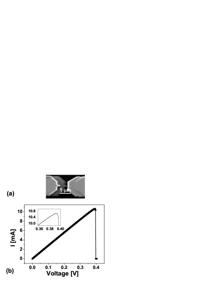
Two kinds of samples are fabricated on top of a 500 nm thick
SiO2 layer on Si. For the first, called ’terrace samples’, we
use shadow evaporation and a resist bridge to obtain different
thicknesses for the leads and the constriction (see Fig.
1a). In the constriction, 15 nm Au is evaporated, while
for the leads 150 nm Au on top of 2 nm Cr is used. To decrease the
constriction length, an extra 50 nm Au is evaporated. This way, a
constriction of about nm (length width)
is obtained. Due to thick gold leads, the total resistance is only
30 (including the wires of the measurement setup). For
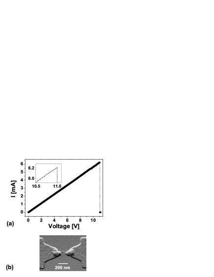
the second kind of samples, called ’bow tie samples’, we define a
constriction in the shape of a bow tie with a minimum width of 20
to 60 nm. In this case, the thickness of the gold in the leads and
the constriction is the same, namely 17 nm. Furthermore, a 3 nm
adhesion layer is used for most of the gold structure. By
evaporating this layer at an angle, we make sure that the Chromium
does not reach the constriction. Therefore, the very center of the
constriction contains gold only.
Electromigration is performed by applying a slowly increasing
voltage (Keithley 230) to the wire, while monitoring the current
(Keithley 6517A). Measurements were done at room temperature (in
air) and at both 77 and 4.2 K (in cryogenic vacuum). After break
down, tunnel currents were determined. In our setup, zero-bias
tunnel resistances up to can be measured.
IV results and discussion
IV.1 Excessive heating during electromigration
A typical graph of an electromigration experiment is shown in Figure 1b. Here, breaking is performed for a ’terrace sample’ (Fig. 1a) by slowly increasing the voltage by 2 mV/s, at 77 K. The initial total resistance (including wiring) is 36 . At about 0.38 V, the current density has reached a value that causes substantial mass flux, starting the formation of a slit. At 0.4 V, the wire finally breaks down. Subsequently, a small tunnel current can be observed, indicating that the gap size is around 1 nm.
A very different result is obtained for the experiment in Fig. 2. For this measurement, performed on a ’bow tie’ sample, we added an extra series resistance. The total initial resistance equals 1780 . Although the graph in Fig. 2a) looks similar to the one in Fig.1b), there are some obvious differences. First, the breaking process is much more abrupt (see insets). Second, the voltage at break down is much higher (11 V vs. 0.4 V). The most dramatic difference is, however, that no tunnel current could be detected after break down. To investigate the gap in more detail, we used atomic force microscopy (AFM). In Figure 2b an AFM picture is shown of the ’bow tie’ sample after the breaking process. The final gap size is approximately 100 nm, and the electrodes have clearly rounded off. Most likely this is due to local melting. Furthermore, there is a set of gold islands in between the electrodes. We note that the presence of such nanoparticles may lead to Coulomb blockade effects.sordan ; hubert ; gonzalez ; houck From Figure 2b we conclude that the break down process has taken place in an uncontrolled manner, leading to high local temperatures (and fields). We shall show below, that the breaking dynamics is strongly correlated with the resistance in series with the constriction, . We note that this resistance constitutes the main difference between the experiments in Figures 1 and 2. Minimizing , results in a much better control of the final gap size, making a feedback system unnecessary.
To demonstrate the significance of , we use a simple model for the constriction (a schematic drawing is shown in Fig. 3). We consider a slit of length l. Its width w(t) and height h(t) are decreasing functions of time, due to gap formation. The total resistance, , is the sum of the constriction resistance, , and a series resistance . In a virtual experiment, we ramp up the voltage until electromigration begins at a bias (at ). A more accurate way of saying that ’electromigration begins’ is to say that the flux of gold atoms, , reaches a certain critical value .speed For this to happen, both the current density and the mobility (related to in eq. (4)) need to be substantial. The mobility is strongly affected by the local temperature, which increases due to Joule heating via . Consequently, electromigration does not start, until a certain combination of current density and local temperature is reached. The latter is directly related to the local dissipation (below, we discuss this in more detail).1D The voltage and local dissipation are related by . Next, we consider the breaking process for , keeping the voltage constant at . Due to electromigration a slit is formed in the constriction, leading to an increasing constriction resistance . Consequently, the local dissipation also increases, according to (in the diffusive regime):
| (6) |
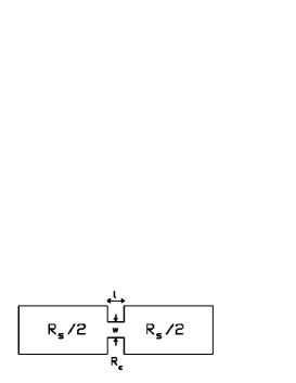
Let us first consider the limit with a small series resistance, . In this case, the dissipated power is always equal to , independent of the width of the constriction. Hence, the local temperature stays close to and the gap grows slowly in time. In the other limit, , the situation is different. At the start of the process (t=0), the local power equals . However, the dissipated power increases rapidly during the breaking process, especially when . In this limit, . Consequently, uncontrollable heating takes place. This can finally lead to melting of the electrodes.ivsource We note that equation (6) only holds in the diffusive regime, where the mean free path of the electrons is much smaller than the dimensions of the contact. Interestingly, as the electromigration process continues, the size of the constriction decreases. Provided that heating is limited, one expects a cross-over from the diffusive to the ballistic transport regime. We will return to this phenomenon in section C.
To have a better control of the final gap size, one has to limit the series resistance within the set-up as well as within the sample itself. For the latter we developed the ’terrace’ samples that connect big leads to the constriction (see Fig. 1a). As compared to the ’bow tie’ samples (see Fig. 2b), this geometry has three advantages. The most important one is to limit the dissipated power during electromigration, by the reduction of . Another advantage is that the voltage needed to break the samples is limited. This is important, since, after break down all the voltage drop will be across the gap. This leads to a high electric field. It is well known that electric fields exceeding 2 V/nm, can cause a reorganization of the electrodes. Depending on the shape of the electrodes, this reorganization can result in a larger gap size.mendez ; huang A third advantage of thick leads, is their use as heat sinks. In this way, the heat can easily flow away from the constriction. By the evaporation of 150 nm Au for the leads, we have a total resistance of typically 30 (including the wiring of the measurement setup).
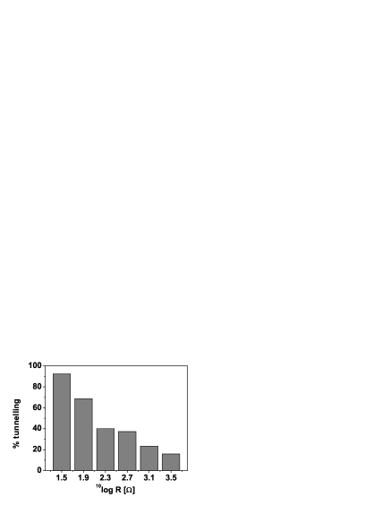
To show the effect of a series resistance experimentally, a variable resistance is inserted in series with the sample. This way, we can check the final gap size as a function of . The result is shown in Fig. 4. We have investigated 142 samples, of both types. The wires were broken by slowly increasing the voltage until a gap occurs. Afterwards, the tunnel resistance at zero bias was measured, in order to make an estimation of the gap size. Zero bias resistances larger than could not be measured, and are counted as ”no tunnelling”. As can be seen from Fig. 4, there is a strong relation between the gap size and the total initial resistance. Considering samples with large series resistances, from , only 15 percent have nanogaps with a measurable tunnel current. Samples with low series resistances, however, give smaller gaps. Decreasing the value for the series resistance to about , gives nanogaps with a measurable tunnel current in more than 90 percent of the cases. From the tunnel current, an estimation can be made of the size of the gaps. These are in the range of 0 to 2 nm.
IV.2 Local temperature during electromigration
For the model discussed above, we assumed that gap formation does not start until a certain critical temperature is reached. To test if this is indeed the case, we performed measurements at 4.2, 77 and 295 Kelvin. We found no clear differences in final gap size. We did observe, however, that a higher critical power is needed, when samples are broken at lower temperatures. This suggests that the local temperature at which electromigration is triggered, is more or less independent of the surrounding temperature. This is as expected, since the mobility of gold atoms is strongly dependent on the temperature (we will discuss this in more detail below).
In order to find the local temperature during electromigration, Tem, we fabricated four terminal devices. Knowledge of Tem is important, since, for molecular electronics, molecules are often put on the sample prior the breaking process. High temperatures could damage the molecules, right where the nanogap will be formed.
To determine the local temperature, the samples were first cooled down to obtain the relation between temperature and (local) resistance (4.2 K T 295 K).lambert ; dumpich ; durkan The electromigration experiment is subsequently performed as follows. First, the voltage is increased till electromigration starts (defined as /s), and kept constant afterwards. An example is shown in Fig. 5. From here on, different processes will influence the local resistance. The most important ones are electromigration, heating and the coalescence of grains. To make an estimation of Tem, it is crucial to deduce only the resistance change due to heating. This was done by interrupting the measurement every couple of minutes, and determining the resistance at low voltage.dumpich Finally, the average local temperature Tem is estimated from the resistance difference at low and high voltage and the (extrapolated) relation between temperature and resistance.
For the trace in Fig. 5, the initial four-terminal resistance was 5.8 (at 77 Kelvin). Setting the voltage to start the breaking process, increases the resistance drastically to about 8 (due to heating). Subsequently, the resistance increases in time, and accelerates just before breaking. Furthermore, the local temperature increases, as predicted by eq. (6). We note that there is always some series resistance, so that heating cannot be taken away completely. However, when high series resistances are used, the temperature does not only reach higher values, it also diverges much faster. This is clearly shown in the insets of Figures 1b and 2a. In Fig. 1b, a slow increase in differential resistance is observed. In contrast, for Fig. 2b, gap formation goes all at once, and the breaking process cannot be resolved.
| Data set | |||
|---|---|---|---|
| A | |||
| B | |||
| C | |||
| D | |||
| E |
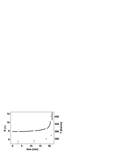
In Fig. 5, the local temperature increases from 77 K to
345 K, when the voltage is set to start the breaking process. The
temperature determined just before break down, , is
about 450 Kelvin. In Table [1], four other data sets are
shown, at different environment temperatures. The temperatures at
which electromigration is triggered are close together, whereas
the variation in the temperature of the environment is about 290
Kelvin. This is a strong indication that gap formation is indeed
due to electromigration (at a critical temperature) and not due to
thermodiffusion via a temperature gradient.durkan
To understand why is rather independent of the
temperature of the sample environment, , we introduce a
simple model. To fit its parameters, we use the data taken at 77 K
(Fig. 5). We rewrite eq. (4), by noting
that is the driving force
due to stress :thin film ; blech
| (7) |
Here is the stress built up over the length L. As long as , the electromigration force is balanced by the stress gradient and the atom flux is zero.thin film ; blech This defines a critical current density , which is independent of temperature, since is temperature independent.sorbello ; verbruggen Using the Einstein relation , where D and c are the diffusion constant and concentration respectively, we can write down the temperature dependence of the atom flux. For the chemical potential we have ln,thin film and for the diffusion constant so that we can write for the phenomenological coefficient: . Here, is the activation energy of gold diffusion on the surface, which is 0.12 eV.Wilson This leads to the following approximation for the atom flux due to the current density:
| (8) |
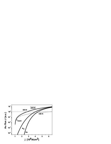
where . For our measurements we use temperatures in between liquid Helium and Room temperature and the applied voltage over the constriction is typically 20 mV or higher. In this range, the inelastic scattering length of the electrons does not exceed the contact size. Therefore, the effective temperature in the contact can be described by , where is a fit parameter.beta We determine from the first temperature point in Fig. 5: K at . Furthermore, we estimate that equals .thin film
Equation [8] implies a strong relation between temperature and mass flux, especially due to the activated behavior. Gap formation starts as soon as the mass flux is large enough, i.e., when reaches a certain value . We define this quantity, in arbitrary units, as . Going back to Fig. 5 with K, we infer that for , we have . From this, we deduce the other parameter . Knowing both and , we can plot as a function of current density j for all three experimental temperatures . This is shown in Fig. 6. For each , we calculate the current density and temperature at which electromigration sets in, , demanding . (For K, this is by definition at with K). For and we find that equals 330 and 420 K, respectively. Hence, increasing the temperature of the environment by 290 K, increases by only 90 K. Related to this is the fact that the critical current density increases with decreasing . Although basic, the model is in rather good agreement with the values of Table [1].
Do previously applied molecules get damaged at these temperatures? As we have shown above, the local temperature just before break down depends on the exact sample design. Also, the maximum temperature molecules can stand, strongly depends on the molecule. At 460 Kelvin, which is in Table [1], most molecules used in molecular electronics, do not get damaged. However, care should clearly be taken. The electromigration process should be controlled either by optimizing the sample design, or by using active feedback. If not, the local temperature increases dramatically as the wire gets thinner and may reach values up to the melting point of gold.
IV.3 Quantized conductance

As we have shown, decreasing the series resistance gives a better control of the final gap size. Another interesting consequence of controlled electromigration, is the possibility to observe the transition between the diffusive and the ballistic regime.strachan If slit formation is a well-defined process, at some point the constriction gets smaller than the inelastic scattering length. In this case, conduction becomes ballistic. This is indeed what we observe in a number of cases. During the breaking process, the sample conductance does not go smoothly to the tunneling regime, but locks in at plateaus equal to integer values of the conductance quantum .bart ; muller An example is shown in Fig. 7. Here, we start with a resistance of about 45 , increase the voltage until we see a change in conductance and, from there on, keep the voltage constant. Slowly, the conductance goes down, to finally stop at 1. At this point, the electromigration process stops automatically, due to the almost perfect transmission of the gold atoms. The corresponding current density is about 57 atom. This is close to the maximum value described elsewhere,mizobata and is much larger than the maximum current density in the diffusive regime. Nevertheless, the electrodes reorganize due to atomic diffusion. Slowly, the contact evolves from a single atom contact to a contact with 3, 5, 8 and 10 gold atoms.statistiek At much higher voltages, it is still possible to break the constriction and obtain a tunnel resistance. We note that we have only observed quantized conductance in samples with minimized . If the power is unlimited, the high temperature prohibits the formation of a single atom contact.
V conclusions
To conclude, we have investigated the role of dissipation during the formation of nanogaps due to electromigration. We find the following. First, some Joule heating is needed for gap formation to begin. The process does not start until a local temperature of typically 400 K is reached. This value is rather independent of the temperature of the surroundings. We relate this phenomenon to the activated behavior of the atomic mobility, which plays a crucial role in this diffusion process. Second, although Joule heating is important to start electromigration, it can also lead to unwanted effects. If no measures are taken, the temperature in the constriction can increase up to the melting point of gold, during slit formation. This leads to large gaps, possibly containing small gold islands. By minimizing the total series resistance of the system, we make sure the temperature keeps low during the electromigration process. In this way, we increased the number of samples with a gap 2 nm to 90 percent, without the use of active feedback. With the improved samples, gap formation is much slower. Hence, it is also possible to observe the transition from the diffusive to the ballistic regime. In a number of cases, contacts have been achieved that consist of only a single or a few atoms.
Acknowledgements.
We thank Gert ten Brink, Niko Tombros, Bernard Wolfs and Siemon Bakker for their assistance and advice. We thank Herre van der Zant and Hubert Heersche for useful discussions. This work was financed by the Nederlandse Organisatie voor Wetenschappelijk Onderzoek, NWO, via a Pionier grant.References
- (1) B. Xu and N.J. Tao, Science 301, 1221, (2003)
- (2) Bumm, L.A., Arnold, J.J., Cygan, M.T., Dunbar, T.D., Burgin, T.P., Jones II, L., Allara, D.L., Tour, J.M. and Weiss, P.S., Science 1996, 271, 1705-1707
- (3) R.H.M. Smit, Y. Noat, C. Untiedt, N. D. Lang, M.C. van Hemert and J.M. van Ruitenbeek, Nature 419 (2002) 906
- (4) D. Dulic, S.J. van der Molen, T. Kudernac, H.T. Jonkman, J.J.D. de Jong, T.N. Bowden, J. van Esch, B.L. Feringa, B.J. van Wees, Phys. Rev. Lett. 91, 207402, (2003)
- (5) J. Reichert, R. Ochs, D. Beckmann, H.B. Weber, M. Mayor and H.V. Lohneysen, Phys. Rev. Lett 88, 176804, (2002)
- (6) H. Park, J. Park, A. K. L. Lim, E. H. Anderson, A. P. Alivisatos, and P. L. McEuen, Nature (London), 407, 57 (2000)
- (7) W. Liang, M. P. Shores, M. Bockrath, J. R. Long, and H. Park, Nature (London), 417, 725 (2002)
- (8) J. Park, A. N. Pasupathy, J. I. Goldsmith, C. Chang, Y. Yaish, J. R. Petta, M. Rinkoski, J. P. Sethna, H. D. Abruna, P. L. McEuen, et al., Nature (London), 417, 722 (2002)
- (9) M. Mahadevan and R.M. Bradley, Phys. Rev. B. 59, 11037 (1999)
- (10) H. Park, A. K. L. Lim, J. Park, A. P. Alivisatos, and P. L. McEuen, Appl. Phys. Lett. 75, 301 (1999)
- (11) K. I. Bolotin, F. Kuemmeth, A. N. Pasupathy, and D. C. Ralph, Appl. Phys. Lett. 84, 3154 (2004)
- (12) D.R. Strachan, D.E. Smith, D.E. Johnston, T.-H. Park, M.J. Therien, D.A. Bonnel and A.T. Johnson, Appl. Phys Lett. 86, 43109 (2005)
- (13) H.B. Heersche, Z. de Groot, J.A. Folk, L.P. Kouwenhoven and H.S.J. van der Zant, A.A. Houck, J. Labaziewicz and I.L. Chuang, Phys. Rev. Lett. 96, 017205, (2006)
- (14) A.A. Houck, J. Labaziewicz, E.L. Chan, J.A. Folk and I.L. Chuang, Nano Letters 5,1685, 9 (2005)
- (15) G. Esen and M. S. Fuhrer , Appl. Phys Lett. 87, 263101 (2005)
- (16) H.S.J. van der Zant et al., Faraday Discuss., 131, 347 (2006)
- (17) S.R. de Groot, Thermodynamics of irreversible processes, North-Holland Publishing company, Amsterdam, (1963)
- (18) S.J. van der Molen, M.S. Welling and R. Griessen, Phys. Rev. Lett. 85, 3882 (2000)
- (19) King-Ning Tu, J.W. Mayer, L.C. Feldman, Electronic thin film science for electrical engineers and materials scientists, Macmillan, New York, (1992)
- (20) J.I. Gonzalez, Tai-Hee Lee, M.D. Barnes, Y. Antoku and R.M. Dickson, Phys. Rev Lett. 93, 147402(2004)
- (21) R. Sordan, K. Balasubradamanian, M. Burghard and K. Kern, Appl. Phys Lett. 87, 013106 (2005)
- (22) For this manuscript we define the starting point of gap formation, when the increase in resistance reaches a speed of 100 /s. We note that for other values, the starting temperature will also change.
- (23) Since we use a 1-dimensional model, the length of our constriction does not change with time.
- (24) A comparison can also be made with a current source (Norton equivalent circuit) and a voltage source (Thevenin circuit). Gold wires with high series resistances are broken as if connected to an ideal current source. As the width of the wire decreases, the current density increases. Constrictions with negligible series resistances are broken as if connected to an ideal voltage source. As the width decreases, the current density stays approximately constant.
- (25) J. Mendez, J. Gomez-Horrero, J.I. Pascual, J.J. Seanz, J.M. Soler and A.M. Baro, J. Vac Sci. Technol. B 14, 1145 (1996)
- (26) D. Huang, F. Yamaguchim, Y. Yamamoto, Jap. Journal Appl. Phys. 37, 3824 (1998)
- (27) M. F. Lambert, M. F. Goffman, J. P. Bourgoin, and P. Hesto, Nanotechnology 14, 772 (2003).
- (28) B. Stahlmecke and G. Dumpich, Defect and Diffusion Forum Vols. 237-240 1163 (2005)
- (29) C. Durkan, M.E. Welland, Ultramicroscopy 82, 125, (2000)
- (30) I.A. Blech, J. Appl. Phys. 47, 1203 (1976)
- (31) R.S. Sorbello, Solid State Phys. 51, 159-231 (1998)
- (32) A.H. Verbruggen, IBM J. Res. Develop. 32, 93 (1988)
- (33) N.T. Wilson, The structure and dynamics noble metal clusters. PhD thesis, University of Birmingham, (Sept. 2000)
- (34) In our measurement range, the applied bias voltage is close to the Debye energy, leading to strong electron-phonon scattering. The inelastic scattering length does not exceed the contact size and the temperature in the contact can be described by the given relation. However, When temperatures around or below 1 Kelvin are considered, and the maximum voltage is in the mV range, electron-electron scattering is the dominant relaxation mechanism. The relation for the temperature becomes . For the measurement at Helium temperature, however, this will give only a minor change in the final maximum temperature (343 K instead of 330 K).
- (35) B.J. van Wees et al., Phys. Rev. Lett. 60, 848 (1988)
- (36) C.J. Muller, J.M. van Ruitenbeek and L.J. de Jongh, Phys. Rev. Lett. 69, 140 (1992)
- (37) J. Mizobata, A. Fujii, S. Kurokawa, A. Sakai, Phys. Rev. B 68, 155428 (2003)
- (38) Since it is not possible to vary the conductance back and forth, as with the mechanically controllable break junctions, we have not performed statistics. However, since the values are exactly equal to the conductance quantum, there is a strong indication that the conductance steps are due to single gold atoms.