Present address: ]Department of Material Science, University of Hyogo, Kohto, Kamogoori-cho 678-1297, Japan
Majority-Carrier Mobilities in Undoped and n-type Doped ZnO Epitaxial Layers
Abstract
Transparent and conductive ZnO:Ga thin films are prepared by laser molecular-beam epitaxy. Their electron properties were investigated by the temperature-dependent Hall-effect technique. The 300-K carrier concentration and mobility were about cm-3 and 440 cm2/Vs, respectively. In the experimental ‘mobility vs concentration’ curve, unusual phenomenon was observed, i.e., mobilities at 1018 cm-3 are significantly smaller than those at higher densities above cm-3. Several types of scattering centers including ionized donors and oxygen traps are considered to account for the observed dependence of the Hall mobility on carrier concentration. The scattering mechanism is explained in terms of inter-grain potential barriers and charged impurities. A comparison between theoretical results and experimental data is made.
I Introduction
Semiconducting materials with a wide band gap, such as SnO2 and In2O3, are commonly used as transparent electrodes in optoelectronics and solar energy conversion technology. Recently, it has been demonstrated that ZnO:Ga may be considered as the next attractive transparent and conductive oxide compounds.
ZnO has a natural tendency to be grown under fairly high-residual n-type in which high concentration of charge carriers of about 1022 cm-3 may be achieved with group-III element doping. Therefore, highly conductive ZnO films are easily prepared.
To date, there have only been a few attempts ellmer_mob1 ; miyamoto_mob1 to model electron transport in doped ZnO. The present publication reports carrier concentration dependence of mobility including an effect of the scattering by ionized donor centers as well as by the grain boundaries fischetti_mob1 ; lowney_mob1 .
II Experimentals
Our samples were grown on lattice-matched ScAlMgO4 (SCAM) substrates by laser molecular-beam epitaxy. ZnO single-crystal and (Ga,Zn)O ceramics targets were ablated by excimer laser pulses with an oxygen flow of torr ohtomo_sst ; makino_sst . The films were patterned into Hall-bars and the contact metal electrodes were made with Au/Ti for n-type film, giving good ohmic contact.
III Results and discussion
The ZnO materials parameters used in the transport theory calculation has been given elsewhere makino_trans . We have not adopted the relaxation time approximation for the mechanisms that involve relatively high-energy transfers, e.g., longitudinal optical phonons. Since Rode’s iterative technique takes a long time to reach its convergence rode_bkmob1 ; fischetti_mob1 , the present computations are based on the variational principle method lowney_mob1 ; ruda_mob1 . The following electron scattering mechanisms are considered: (1) polar optical-phonon scattering, (2) ionized-impurity scattering, (3) acoustic-phonon scattering through the deformation potentials, and (4) piezo-electric interactions seeger_bkmob1 ; lowney_mob1 ; ruda_mob1 .
The values of are 440 cm2/Vs and 5,000 cm2/Vs at 300 and 100 K, respectively. We have derived partial mobilities by accounting for respective scattering mechanisms in the nondegenerate (undoped) limit. The total electron mobility was calculated by combining all of the partial scattering mechanisms. Our experimental data are in reasonably good agreement with theory. The mobility limit at 300 K is about 430 cm2/Vs.
On the other hand, the situation is somewhat different for the cases of Ga-doped n-type films makino_int_Ga . Figure 1 shows 300-K experimental mobilities plotted against carrier concentration ().
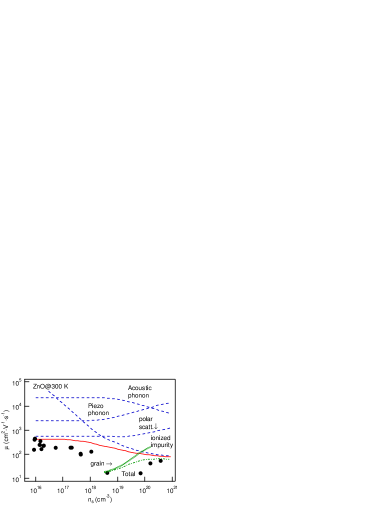
The mobilities of doped films are significantly smaller than those of undoped one makino18 ; makino19 . Obviously, this tendency can be qualitatively attributed to the increased density of impurities. For quantitative comparison, partial mobilities are calculated and given in Fig. 1 by dashed lines. We have taken the effects of screening for both ionized impurities and polar optical phonon scattering into account. Polar interactions reflecting the ionicity of the lattice are dominant in scattering mechanism, while, at heavier doping levels, ionized impurity scattering controls inherent mobility limit curve ruda_mob1 ; lowney_mob1 . The experimental data agree well with our calculation (solid curve) except for the intermediate concentration range. Particularly, our model could not reproduce a relative minimum in the “ vs ” curve, which has been experimentally observed in this intermediate doping range. The situation at > 1020 cm-3 could be improved probably if the effects of non-parabolic band structure as well as of clustering of charged carriers would be taken into account ellmer_mob1 .
The presence of grain boundaries and trapped interface charges in semiconductors leads to inter-grain band bending and potential barriers pisarkiewicz1 . Under specific conditions, this effect may be so prominent that it can significantly influence the scattering process of free carriers, giving rise to a considerable reduction in the Hall mobility.
It is well established that grain boundaries contain fairly high density of interface states which trap free carriers from the bulk of the grains. Such a grain may be thought of as a potential barrier for electrons characterized by its height and width for a given number of traps per unit area.
The contribution (boundary partial mobility) to the total mobility that comes from the scattering at grain boundaries is thermally activated and can be described by the well-known relation:
| (1) |
With , where is the charge of a trap (in this case ). By solving the Poisson equation, one obtains:
| (2) |
where is the concentration of ionized donors and other nomenclatures take conventional meanings.
Therefore in our model, we have two free parameters, i.e., and , that can be determined from the best fit of
| (3) |
to the experimental data , where (the full curve in Fig. 1) refers to all the partial mobilities except for .
We calculated the barrier height according to Eq. (2). At low electron concentrations is large, so we can infer that in that case the Hall mobility is barrier limited.
We compared our theoretical results with those experimentally determined. The best fit of our model including all of the contributions to the experimental dependence of on n for ZnO films is presented in Fig. 1. The best fit yields and 2 nm.
Partial contribution from is separated by a dash-dotted curve in Fig. 1 to give a better understanding of the scattering mechanism. The contribution from barrier-limited scattering is of no importance as far as high electron concentrations are concerned. Unfortunately, our model can be applied only to the case of degenerate semiconductor regime.
IV Summary
The electrical properties of wide band gap, degenerate ZnO thin films are investigated. The experimental dependences of the Hall mobility on the electron concentration is explained mainly in terms of scattering by grain boundaries and charged impurities. Oxygen accumulated in the grain boundaries plays an important role in the scattering mechanism.
acknowledgements
One of the authors (T. M.) thanks H. S. Bennett of NIST, D. L. Rode of Washington University, St. Louis, USA, H. Ruda of University of Toronto, Canada, and B. Sanborn of Arizona State University, USA for helpful discussion. Thanks are also due to Shin Yoshida for technical assistance during our experiments.
References
- (1) K. Ellmeer, J. Phys. D. 34, 3097 (2001).
- (2) K. Miyamoto, M. Sano, H. Kato, and T. Yao, Jpn. J. Appl. Phys. 41, L1203 (2002).
- (3) M. V. Fischetti, Phys. Rev. B 44, 5527 (1991).
- (4) J. R. Lowney and H. S. Bennett, J. Appl. Phys. 69, 7102 (1991).
- (5) A. Ohtomo and A. Tsukazaki, Semicond. Sci. & Technol. 20, S10 (2005).
- (6) T. Makino, Y. Segawa, M. Kawasaki, and H. Koinuma, Semicond. Sci. & Technol. 20, S78 (2005).
- (7) T. Makino, Y. Segawa, A. Tsukazaki, A. Ohtomo, and M. Kawasaki, Appl. Phys. Lett. 87, 022101 (2005).
- (8) D. L. Rode, Semiconductors and Semimetals 10, 1 (1975).
- (9) H. E. Ruda and B. Lai, J. Appl. Phys. 68, 1714 (1990).
- (10) K. Seeger, Semiconductor Physics: An Introduction, 8 ed. (Springer Verlag, Berlin, ADDRESS, 2002).
- (11) T. Makino, Y. Segawa, A. Tsukazaki, A. Ohtomo, S. Yoshida, and M. Kawasaki, Appl. Phys. Lett. 85, 759 (2004).
- (12) T. Makino, C. H. Chia, Y. Segawa, A. Ohtomo, K. Tamura, M. Kawasaki, and H. Koinuma, Phys. Status Solidi (B) 299, 853 (2002).
- (13) T. Makino, K. Tamura, C. H. Chia, Y. Segawa, M. Kawasaki, A. Ohtomo, and H. Koinuma, Phys. Rev. B 65, 121201(R) (2002).
- (14) T. Pisarkiewicz, K. Zakrzewska, and E. Leja, Thin. Solid. Films 174, 217 (1989), -223.