Present adress: ]Department of Physics, Northern Illinois University, De Kalb, IL 60115
Giant anisotropy of Zeeman splitting of quantum confined acceptors in Si/Ge
Abstract
Shallow acceptor levels in Si/Ge/Si quantum well heterostructures are characterized by resonant tunneling spectroscopy in the presence of high magnetic fields. In a perpendicular magnetic field we observe a linear Zeeman splitting of the acceptor levels. In an in-plane field, on the other hand, the Zeeman splitting is strongly suppressed. This anisotropic Zeeman splitting is shown to be a consequence of the huge light hole-heavy hole splitting caused by a large biaxial strain and a strong quantum confinement in the Ge quantum well.
pacs:
71.18.+y, 71.70.Fk, 73.21.FgSpintronic and quantum computing aws02 ; los98 are novel device concepts relying on quantum mechanical coherence. Si/Ge-based systems are promising candidates offering long spin coherence times tyr05 ; tyr03 , fast operations, and a well-established record of scalable integration. These important properties are also crucial requirements los98 ; pre98 ; sou03 for implementing multi-qubit operations in a future quantum computer. One concept that may form the technological basis of a quantum computer is the spin-resonance transistor (SRT) kan98 . Vrijen et. al. vri00 proposed an SRT where the electron spin manipulation is realized using the change in -factor between Si-rich and Ge-rich environments of a Si/Ge-heterostructure. However, engineering the -factor in such systems is complicated by the fact that the electron states in Si are in the valleys whereas in Ge the electrons are located in the valleys bar03 . This problem does not arise for the valence band states, as both Si and Ge have their valence band maximum at the point. Thus, valence band states in Si/Ge are a promising choice for -factor engineering in search for spin manipulation.
In this paper we have analyzed the -factor of shallow acceptor levels in a Si/Ge-heterostructure by resonant-tunneling spectroscopy. We find that their effective -factor is highly anisotropic, giving a large Zeeman splitting of the acceptor states in a perpendicular field, whereas we cannot resolve any Zeeman splitting in in-plane fields up to 18 T. This giant anisotropy provides the possibility to tune the coupling of the holes to an external magnetic field by a gate-controlled shift of the hole wave function mal01 in spintronic devices.
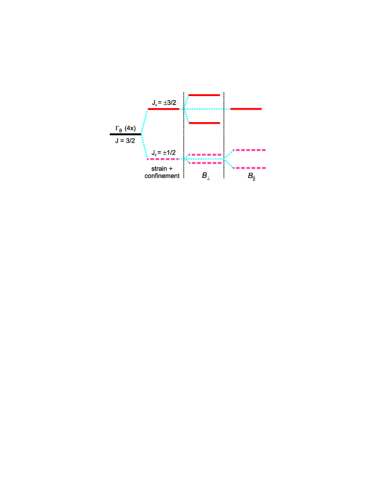
For a proper understanding of acceptor levels it is essential to take into account the fourfold degeneracy of the valence band at the point (Fig. 1) which reflects the fact that the bulk valence band edge in these materials is characterized by an effective angular momentum lut56 ; win03 . As the symmetry of the crystal is reduced due to biaxial strain and a confinement potential, the degenerate states split into heavy-hole (HH) subbands with and light-hole (LH) subbands with . Here, the quantization axis for the angular momentum is the -axis perpendicular to the epitaxial layer. So both parameters, the confinement potential and the built-in strain, substantially influence the energy levels of an acceptor in a quantum well (QW) mas85 ; ales02 . In a magnetic field orientated perpendicular to the epitaxial layer we get a Zeeman splitting of HH and LH states, , where is the -factor of the HH (LH) states in a perpendicular field and is the Bohr magneton. But for an in-plane magnetic field the linear Zeeman splitting of HH states is suppressed because there is no -induced direct coupling between these states, , where is the vector of spin matrices kes90 ; gla90 ; lin91 ; gol93 . This does not apply for LH states which show a significant Zeman splitting . We emphasize that the vanishing Zeeman splitting of HH states in a parallel field reflects the fact that the HH-LH splitting in our samples is much larger than the maximal Zeeman energies ( meV) win03 .
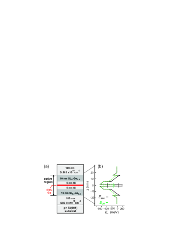
Figure 2 shows the layer sequence and the valence band profile of our samples. They are prepared by growing a 100 nm thick Si:B layer ( cm-3) on a (001) -Si substrate. The active region of the samples consists of two 10 nm thick SiGe QWs separated by a 10 nm thick Si barrier. In the center of the Si barrier a 4 monolayers (ML) thick Ge QW is embedded. Finally, the active region is capped with 100 nm Si:B ( cm-3). For the dc-transport measurements we have fabricated diodes with lateral diameters of 1 m. Measurements were performed at temperatures down to mK and using magnetic fields up to 18 T.
Figure 3(a) shows a typical current-voltage () characteristic of a diode at mK. A staircase structure is observed that is even better resolved in the differential conductance () curve shown in Fig. 3(b). The steplike increase of the current is in a bias range which is about 300 mV below the onset of resonant tunneling of holes through the 2D subbands of the central Ge QW so that this mechanism cannot explain the current steps. We attribute these current steps in the pA-range to tunneling processes of holes through zero-dimensional acceptor levels of Boron dopant-atoms which have migrated into the Ge QW from the highly doped Si:B contact regions.
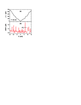
A resonant tunneling process through an acceptor level occurs each time is in resonance with the Fermi energy of the emitter. The bias position of a current step is given by , where is the bias-to-energy conversion coefficient. We determine from the temperature-dependent broadening of the current step edges. As a measure of this broadening, we use the full width at half maximum of the corresponding differential conductance peaks, [see Fig. 3(b)]. It increases according to , where the term stems from the broadening of the Fermi function characterizing the carrier distribution. Using this equation we obtain for several peaks in both bias polarities.
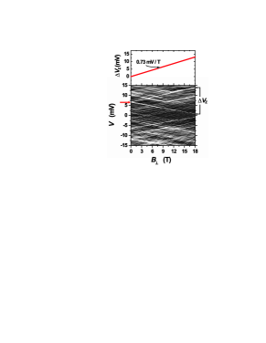
Figure 4 shows a gray-scale plot of the differential conductance as a function of an external magnetic field orientated perpendicular to the epitaxial layer, . In the voltage range from mV to 15 mV the conductance maxima exhibit a linear splitting as a function of . All levels show accurately the same splitting, as indicated by the parallel evolution of the conductance maxima. As an example, the upper panel of Fig. 4 shows the splitting of the conductance maximum at 6.5 mV. The gradient of the splitting is mV/T. We attribute the linear splitting to the Zeeman splitting of the HH sublevels, . The -factor can be determined using
| (1) |
With and mV/T we obtain . This value agrees well with optically measured -factors soe73 ; bro79 of group-III impurities such as B in Ge. This confirms the assumption that the observed levels belong to Boron dopant-atoms which have diffused from the heavily doped contact regions into the Ge QW.
Using the dependence of the conductance we can obtain an upper limit for the radial extent of the wave function of a hole bound to an acceptor level. According to first-order perturbation theory, a ground state acceptor level is affected by a diamagnetic shift , with the HH effective mass of Ge. (We neglect here the modifications of the hole wave functions caused by the confinement in the narrow QW.) But even at T a diamagnetic shift of the levels cannot be observed in our measurements, only the contribution of the linear Zeeman splitting can be seen in Fig. 4. This implies that the diamagnetic shift of the acceptor level is smaller than the width meV of the conductance peak at 50 mK so that must be smaller than nm. Therefore, of the acceptor wave functions in the thin Ge QW is of the same order as the QW width. We remark that Bastard bas81a derived a simple model to estimate for an impurity in a narrow QW which yields for our system parameters , where nm is the effective Bohr radius for heavy holes in Ge.
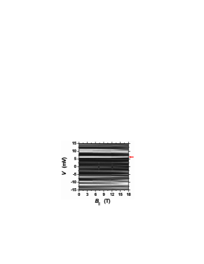
Next we present in Fig. 5 our results for the measured conductance in an in-plane magnetic field . While we saw in Fig. 4 that gives rise to a significant Zeeman splitting of the acceptor levels linear in , it is most remarkable that up to 18 T most conductance maxima are not at all influenced by an in-plane magnetic field . The conductance maximum at 6.5 mV, which exhibits a pronounced linear splitting for (arrow in Fig. 4), does not show any splitting in the case of an in-plane magnetic field (arrow in Fig. 5). If a splitting exists, it must be smaller than the width of the conductance peak which is about 0.35 meV temprat here.
The giant anisotropy of the Zeeman splitting is a consequence of the effective spin of the valence band states (Fig. 1). For a detailed interpretation of our experimental results, we have performed self-consistent calculations in the multiband envelope-function approximation win03 of the valence band profile of the active region using the nominal growth parameters. The results of the calculation are plotted in Fig. 2(b). The solid (dashed) lines show the HH (LH) subbands and the strain-split effective potentials for these states. The calculation predicts a splitting of the lowest HH and LH subbands of about 200 meV. This huge HH-LH splitting is caused by the strong quantum confinement of the thin Ge layer and the large biaxial strain due to the lattice mismatch between Ge and Si.
The behavior of the HH states in our device is in sharp contrast to electron states for which it is well-known that the Zeeman splitting is proportional to the total magnetic field irrespective of the orientation of relative to the epitaxial layer. Furthermore, confinement potential and strain do not affect the Zeeman energy of electron states. In the case of HH states, on the other hand, the Zeeman splitting in a field competes with HH-LH splitting; Zeeman splitting is the smaller the larger the HH-LH splitting and vice versa win03 . The appropriate situation can be created in a narrow QW or by application of uniaxial or biaxial stress. Our samples satisfy both of these requirements so that we obtain a huge HH-LH splitting, as can be seen in the band profile in Fig. 2(b), resulting in a vanishingly small Zeeman splitting in a field . This explains why we do not observe a Zeeman splitting in Fig. 5.
In the discussion of Fig. 1 only the isotropic part of the bulk Zeeman term was taken into account lut56 ; win03 . This is the dominant term. The anisotropic part is typically two orders of magnitude smaller than the isotropic part and the calculations predict for our structure that it gives rise to a linear splitting with meV at T. Such a small splitting cannot be resolved in our experiment due to the width of the conductance peaks. It corresponds to which is almost two orders of magnitude smaller than
In rare cases of conductance peaks we see a slightly different behavior. In Fig. 5 two conductance maxima at mV and mV indicate a small nonlinear splitting above 10 T. If HH-LH coupling is taken into account, we get a splitting cubic in and inversely proportional to the HH-LH splitting, (Ref. win03 ). For a fully strained system [Fig. 2(b)] the calculated splitting due to this term is even smaller than the splitting due to the anisotropic Zeeman term. However, it is conceivable that the levels showing a splitting nonlinear in are related to shallow acceptors situated in sample regions of slightly relaxed strain (e.g., close to misfit dislocations). In these regions the HH-LH splitting is thus reduced and the cubic Zeeman splitting increases for these levels. This can explain why a nonlinear splitting is observable for the two conductance peaks at mV, but not for the majority of the conductance resonances which are due to impurities in highly strained regions.
In conclusion, we have performed a detailed study of Zeeman splitting of shallow acceptor levels in a thin Si/Ge/Si quantum well, by using resonant tunneling spectroscopy. In a magnetic field orientated perpendicular to the layer a large linear Zeeman splitting can be observed for magnetic fields up to 18 T. In an in-plane magnetic field the Zeeman splitting is suppressed. The giant anisotropy of the Zeeman splitting is a consequence of the huge heavy hole-light hole splitting produced by a large biaxial strain and a strong quantum confinement in the narrow Ge quantum well. It opens a new way to -factor engineering for spintronics and quantum computing.
References
- (1) D. D. Awschalom, D. Loss, and N. Samarth, Semiconductor Spintronics and Quantum Computations (Springer, Berlin, 2002).
- (2) D. Loss and D. P. DiVincenzo, Phys. Rev. A 57, 120 (1998).
- (3) A. M. Tyryshkin, S. A. Lyon, W. Jantsch, and F. Schäffler, Phys. Rev. Lett. 94, 126802 (2005).
- (4) A. M. Tyryshkin, S. A. Lyon, A. V. Astashkin, and A. M. Raitsimring, Phys. Rev. B 68, 193207 (2003).
- (5) J. Preskill, Proc. R. Soc. Lond. A 454, 385 (1998).
- (6) R. de Sousa and S. Das Sarma, Phys. Rev. B 67, 033301 (2003); R. de Sousa and S. Das Sarma, Phys. Rev. B 68, 115322 (2003).
- (7) B. E. Kane, Nature 393, 133 (1998); A. J. Skinner, M. E. Davenport, and B. E. Kane, Phys. Rev. Lett. 90, 087901 (2003).
- (8) R. Vrijen, E. Yablonovitch, K. Wang, H. W. Jiang, A. Balandin, V. Roychowdhury, T. Mor, and D. DiVincenzo, Phys. Rev A 62, 012306 (2000).
- (9) F. A. Baron, A. A. Kiselev, H. D. Robinson, K. W. Kim, K. L. Wang, and E. Yablonovitch, Phys. Rev. B 68, 195306 (2003).
- (10) I. Malajovich, J. J. Berry, N. Samarth, and D. D. Awschalom, Nature 411, 770 (2001).
- (11) J. M. Luttinger, Phys. Rev. 102, 1030 (1956).
- (12) R. Winkler, Spin-Orbit Coupling Effects in Two-Dimensional Electron and Hole Systems (Springer, Berlin 2003).
- (13) W. T. Masselink, Y.-C. Chang, and H. Morkoc, Phys. Rev. B 32, 5190 (1985).
- (14) V. Ya. Aleshkin, V. I. Gavrilenko, D. B. Veksler, and L. Reggiani, Phys. Rev. B 66, 155336 (2002).
- (15) H. W. van Kesteren, E. C. Cosman, W. A. J. A. van der Poel, and C. T. Foxon, Phys. Rev. B 41, 5283 (1989).
- (16) E. Glaser, J. M. Trombetta, T. A. Kennedy, S. M. Prokes, O. J. Glembocki, K. L. Wang, and C. H. Chern, Phys. Rev. Lett. 65, 1247 (1990).
- (17) S. Y. Lin, H. P. Wei, D. C. Tsui, J. F. Klem, and S. J. Allen, Jr., Phys. Rev. B 43, 12110 (1991).
- (18) G. Goldoni and A. Fasolino, Phys. Rev. B 48, 4948 (1993).
- (19) H. P. Soepangkat and P. Fisher, Phys. Rev. B 8, 870 (1973).
- (20) J. Broeckx, P. Clauws, K. van den Steen, and J. Vennik, J. Phys. C: Solid State Phys. 12, 4061 (1979).
- (21) G. Bastard, Phys. Rev. B 24, 4714 (1981).
- (22) The transport measurements in Fig. 5 were performed at 1 K which resulted in a full width at half maximum of the corresponding conductance peaks of 0.35 meV.