Step by step capping and strain state of GaN/AlN quantum dots studied by grazing incidence diffraction anomalous fine structure
Abstract
The investigation of small size embedded nanostructures, by a combination of complementary anomalous diffraction techniques, is reported. GaN Quantum Dots (QDs), grown by molecular beam epitaxy in a modified Stranski-Krastanow mode, are studied in terms of strain and local environment, as a function of the AlN cap layer thickness, by means of grazing incidence anomalous diffraction. That is, the X-ray photons energy is tuned across the Ga absorption K-edge which makes diffraction chemically selective. Measurement of hkl-scans, close to the AlN Bragg reflection, at several energies across the Ga K-edge, allows the extraction of the Ga partial structure factor, from which the in-plane strain of GaN QDs is deduced. ¿From the fixed-Q energy-dependent diffracted intensity spectra, measured for diffraction-selected iso-strain regions corresponding to the average in-plane strain state of the QDs, quantitative information regarding composition and the out-of-plane strain has been obtained. We recover the in-plane and out-of-plane strains in the dots. The comparison to the biaxial elastic strain in a pseudomorphic layer indicates a tendency to an over-strained regime.
pacs:
61.10.Eq, 61.10.Ht, 61.10.Nz, 61.46.+w, 68.65.HbI Introduction
Most of the interest in the improvement of the growth techniques for III-V semiconductor nanostructures originates from the fact that the quantum confinement of carriers leads to unique optoelectronic performances. The confinement in 1 dimension, that is the growth of quantum wells (QWs), has been brought under control for a variety of systems, leading to QWs based optoelectronic devices, such as nitride QWs laser diodes Ponce97 . However, due to the large densities of defects in the III-nitride materials Wu98 , the emission efficiency of such devices is strongly altered by the increasing of temperature. As an alternate way to overcome that difficulty, carriers may be confined in regions free of any defect Arakawa82 , such as self-organized quantum dots (QDs). For reasonable optoelectronic efficiency, a simultaneous control over the size, size distribution, nucleation sites, density and structure of the QDs is required. In the InAs/GaAs system, room temperature ultraviolet lasers Ledentsov02 could be achieved once these requirements were satisfied. This article focuses on the GaN/AlN system, for which the overall control of the QDs characteristics still remains a challenge. In the last few years, Molecular Beam Epitaxy (MBE) has recently been of particular interest with the improvement of QDs density control, using the Stranski-Krastanow (SK) growth mode Daudin97 ; Adelmann04 ; Brown04 and derivatives Gogneau03 ; Adelmann02 ; Damilano99 . Size homogeneization of the QDs was achieved using vertical correlation through strain fields Tersoff96 ; Chamard03 ; Coraux05a .
Alternatively, new efforts are made to understand the effects of the QDs capping by AlN, which strongly modifies the strain state in the QDs Daudin05 ; Coraux05a , and therefore plays a decisive role in the modification of the optical properties. Moreover, this topic raises a fundamental interest regarding the physics of strain accomodation between a QD and its capping.
Many complementary methods have been applied to quantitative strain characterization in nanostructures Stangl04 . This is true for Grazing Incidence X-Ray Diffraction (GIXRD), which can be made chemically sensitive when carried out as a function of the energy across the absorption edge of an element. This technique is known as anomalous diffraction Hodeau01 and is suitable (a) to localize some element in reciprocal space Hendrickson91 , (b) to identify the local environment of an atom Stragier92 , and (c) to determine the composition of an iso-strain region selected by diffraction Letoublon04 .
In this article we present a comprehensive strain analysis of the capping of GaN QDs by AlN. More precisely, we study the in-plane and out-of-plane strain state in the QDs as a function of the AlN capping thickness, by means of grazing incidence anomalous x-ray diffraction at the Ga K-edge (10.367 keV), around the reflection.
The MBE preparation of the set of samples to be analyzed is presented in section II. The strain characterisation technique, by Grazing Incidence Diffraction Anomalous Fine Structure (GIDAFS), is detailled in section III. The strain and composition informations obtained using different aspects of GIDAFS, namely Multi-wavelength Anomalous Diffraction (MAD), Extended Diffraction Anomalous Fine Structure (EDAFS) oscillations and diffraction anomalous lineshape analysis are given in section IV, V, and VI.
II Samples
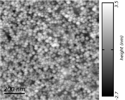
The samples were grown in a MECA 2000 MBE chamber, equiped with standard effusion cells providing the Ga and Al fluxes, and a radiofrequency plasma cell providing the active nitrogen flux. The substrate were thick AlN layers deposited by Metal Organic Chemical Vapor Deposition on sapphire Shibata03 . The substrate temperature was fixed at . Prior to the growth of the QDs, 10 nm thick AlN buffers were grown. The QDs growth was achieved in the modified SK growth mode Gogneau03 ; Adelmann02 , by depositing 6 GaN monolayers (MLs) under Ga-rich conditions. This resulted in the formation of a Ga bilayer at the surface inhibiting the 2D/3D transition even above the usual 2 MLs critical thickness for the 2D/3D transition in the SK growth mode Daudin97 . The thermal evaporation under vacuum of the Ga bilayers led to the transition of the 2D GaN layer into 3D QDs Gogneau03 ; Adelmann02 connected by a 2 MLs thick Wetting Layer (WL). A set of 5 samples was grown, with increasing AlN capping : 0, 2, 5, 10, and 20 MLs. Figure 1 shows a Atomic Force Microscopy (AFM) image of free standing dots sample. The height of the QDs was evaluated to , their diameter to , leading to an aspect ratio of about 0.2. The QDs density was found as high as , that is QDs are almost adjacent.
III GIDAFS measurements
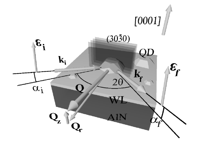
Grazing Incidence Diffraction Anomalous Fine Structure (GIDAFS) at the Ga K-edge (10.367 keV) was performed at the French Collaborative Research Group beamline BM2 at the European Synchrotron Radiation Facility (ESRF) by using the 8-circle diffractometer equipment. We measured the diffuse scattering intensity, in grazing incidence and exit, close to the in-plane Bragg reflection of the AlN substrate (radial scans), at energies close to the Ga K-edge. Figure 2 sketches the experimental set-up. The samples were mounted in the vertical plane, i.e. the polarization vector of the incident photon beam was perpendicular to the sample surface (0001). The incidence angle was lower than the bulk AlN critical angle (at ) for which the total reflection regime takes place. Such conditions were used to enhance the weak contribution of the encapsulated dots layer with respect to that of the substrate. The diffraction geometry was chosen in such a way to keep the scattering vector in the vertical plane. The diffraction point-detector was a scintillator and the slits were opened so as to measure the integrated intensity over the grazing exit angle . A photodiode measuring the fluorescence yield of an in-vacuum 4 Ti-foil was used to monitor the incoming x-ray beam. Two kinds of scans were performed : a) h-scans (radial) in the range 2.9-3.05 for 12 energies, from 10.272 to 10472 keV, i.e. close to the Ga K-edge, and b) energy scans at fixed scattering vector (Q) corresponding to the maximum of the QDs contribution to the diffuse scattering (i.e. at the maximum of the partial structure factor profile extracted from the multiwavelength h-scans, see the following section and ref. Letoublon04 ). The energy scans were recorded in a large energy interval, typically 1 keV , with an energy step from 1 to 2 eV, to allow the quantitative analysis of both the edge and the extended oscillations.
IV MAD analysis
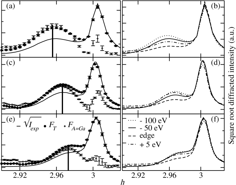
The solid lines in fig. 3(a,c,e) show square root intensities along direction (h-scan) close to the reflection as a function of the AlN coverage. These h-scans are related to both the in-plane strain state and size. With no AlN coverage, one observes a diffuse-scattering peak ascribed to QDs slightly strained by the AlN buffer and substrate. As the AlN coverage increases (from (a) : free standing QDs to (e) : 10 MLs AlN coverage), this peak is progressively shifted towards higher h values and gets mixed to the AlN buffer peak. Further analysis was made possible by distinguishing the GaN and AlN contributions, using MAD measurements Letoublon04 ; Hodeau01 ; Hendrickson91 . Figures 3(b,d,f) show some of the square root diffracted intensities measured for increasing AlN coverage, across the Ga K-edge, taking advantage of the Ga anomalous effect to localize the Ga contribution along . The Ga scattering factor can be written as , where and are the Ga real and imaginary anomalous (resonant) scattering corrections, is the Ga Thomson scattering factor. From MAD measurements, the Ga partial structure factor of phase , that includes the Thomson scattering of all anomalous atoms (Ga), can be retrieved. The retrieval shall be run in the framework of the Distorted Wave Born Approximation, taking into account scattering paths involving the reflection from the layer supporting the dots Pietsch04 ; Schmidbauer05 . We recorded the diffracted intensity integrated over the exit angle , between 0 and , and therefore collected all the scattering paths. Discarding the energy dependence of the reflection coefficients at the Ga K-edge, as a consequence of the small Ga amount (6 equivalent MLs), the recorded intensity corrected for fluorescence, , is proportional to the total square structure factor :
| (1) |
where . Figure 4 shows the total and partial structure factors relations in the complex plane. The partial structure factor of phase that includes the overall contribution of non anomalous atoms and the Thomson scattering of all anomalous atoms, , as well as , can be extracted for all h values, without any structural model by fitting eq. 1 to the experimental data with the NanoMAD algorithm FavreNicolin05 .
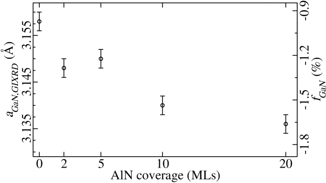
As shown in fig. 3(a,c,e), and were extracted. The position of the diffuse peak maximum is inversely proportional to the in-plane average lattice parameter , since the distance between GaN planes is with , for the AlN substrate peak used as a reference. Figure 5 shows the evolution of the in-plane lattice parameter as a function of the AlN cap thickness. The uncapped QDs are partially in-plane relaxed, with an average strain relative to bulk GaN, , with . The QDs are then progressively in-plane compressed by the AlN capping, but remain slightly relaxed, , compared to pseudomorphic GaN ().
V EDAFS analysis
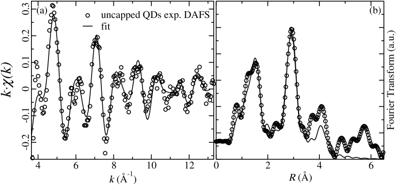
Out-of-plane information can be achieved by quantitative analysis of the Grazing incidence Diffraction Anomalous Fine Structure (GIDAFS) oscillations in the extended region above the edge (EDAFS). Figure 6(a) shows for free standing QDs the oscillatory contribution to the DAFS spectrum, extracted and normalized to the smooth atomic background () :
can be written as where is a normalization factor that depends on crystallography and is calculated from the parameters and (see eq. 1) , is in the first order approximation of the diffracted anomalous fine structure Proietti99 :
| (2) |
where the j label runs over the different anomalous sites A (the Ga sites, A=Ga), and are crystallographic weights. The term () in eq. 2 is the oscillatory part of the resonant atomic scattering factor (), it is related to the local atomic environment of the resonant atom. is formally identical to the Extented X-ray Absorption Fine Structure (EXAFS) oscillations of atom . In the present case, i.e. one statistical equivalent site, can be rewritten as a function of the virtual photoelectron wave vector modulus k in a form that is similar to the well known EXAFS formula Proietti99 :
| (3) |
where runs over all the possible virtual photoelectron scattering paths, is the effective length of path , is the net scattering photoelectron phase shift.
The analysis can be performed according to the standard criteria and available codes for EXAFS, provided that crystallographic phases and amplitude correction factors are taken into account (for more details see references Proietti99 ; Renevier03 ). The EDAFS analysis has been carried out by using the FEFF8 code Ankudinov98 to generate theoretical phases and amplitudes, taking into account beam polarization, for a radius GaN cluster. In order to address for the possible presence of Al atoms in the QDs or at the substrate and capping interface, Ga-Al and Ga-N-Al scattering paths were considered by calculating an AlN cluster with the Ga central atom as absorber. The Artemis interface to the IFEFFIT package Newville95 was used to fit theoretical computations to the experimental data.
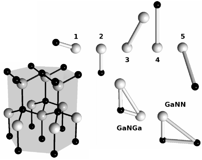
The EDAFS spectra were Fourier Transformed in the k-range 3-10 , and the fit was performed in R-space (real space), using 4 next neighboring shells (I-IV). As an example, we show the best fit curves for free standing QDs in fig. 6(a) and 6(b), compared to the experimental raw data. Six Single Scattering paths (SS) and four 4 Multiple Scattering (MS) paths were found to be relevant in this range (see fig. 7)
-
1.
, in-plane, I shell path, corresponding to the 3 Ga-N bonds of the tetrahedron that are nearly in-plane,
-
2.
, out-of-plane, I shell path, corresponding to the fourth Ga-N bond of the tetrahedron, lying along c-axis,
-
3.
, II shell, out-of-plane path, corresponding to 6 Ga atoms at a distance that is a combination of and , , where is the in-plane lattice parameter obtained with the Grazing Incidence (and exit) X-ray Diffraction experiment (see IV),
-
4.
, III shell path, corresponding to one N atom along direction,
-
5.
, IV shell path, corresponding to 6 N nearly in-plane atoms,
-
6.
MS paths consisting of triangular paths Ga-N-N and Ga-N-Ga.
The ”in-plane” statement refers to the surface or growth plane, and all the scattering paths, except the first one, were expressed in terms of a and c cell parameters, as requested by the hexagonal cell symmetry.
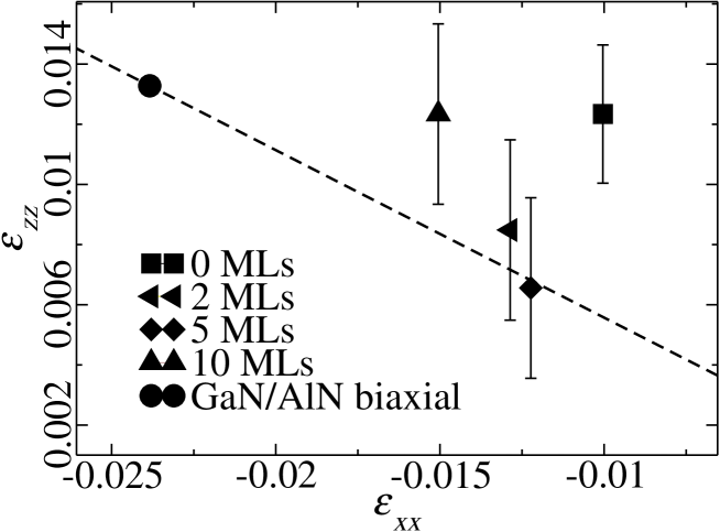
We performed the fit by fixing the a parameter (in-plane) to the values found by diffraction, , letting the c parameter vary according to the hexagonal symmetry. The Ga-N first shell distances were let free to vary independently of a and c since, as it is well known, the Vegard’s law is far from being valid for semiconductor alloys, in which the bond-bending mechanism is dominant compared to bond-stretching Romanato98 . The presence of Al is taken into account by adding the correspondent scattering paths in which Al substitutes for Ga as Next Nearest Neighbour (NNN) and mutiplying the amplitude by a factor for Al and () for Ga. The best fit parameters are shown, for the whole set of samples in table 1, where we also report, as a reference, the bulk and pseudomorphic values for GaN Schulz97 . The Ga-Al distance was also let free to vary and the values found were close to the Al-Al NNN distance. Since the Al content is found to be zero within the statistical errors, the Al-Al NNN distance was not reported in the table. Starting from the fit results, the in-plane and out-of-plane strain were calculated, with respect to relaxed (bulk) GaN, as and . vs for the different samples studied are sketched in fig. 8. These values are compared to the biaxial elastic behaviour for pseudomorphic GaN on AlN (straight line), which corresponds to , with the elastic coefficients and values from reference Andreev00 .
We observe the following general findings :
-
1.
the Ga-N first shell in-plane and out-of-plane distances show to be very close to each other, within the fit errors (0.01 ), in agreement with previous studies Acapito02 ,
- 2.
-
3.
the values range from 5.22 to 5.25 , that is quite large compared to the values foreseen by the elastic regime of a pseudomorphic GaN layer, as apparent in fig. 8 where the experimental points fall above the elasticity curve.
As expected, the uncapped QDs do not follow a biaxial strain behaviour, in reason of the presence of free surface. However, capping by a thin layer (2-5 MLs) of AlN should favor the evolution towards the biaxial case for at least two reasons : a) first of all, capping results in a size decrease of the dots, i.e. an aspect ratio reduction associated with a relative increase of the biaxial component of the strain Gogneau04 ; b) furthermore we speculate that the possible wetting of the QDs by AlN, which will be discussed in section VI, strongly tends to reduce the relaxation through the free surface, which also results in a relative increase of the biaxial component of the strain. Besides these considerations, it is worth noting that the plastic relaxation process of AlN deposited on GaN which is characterized by a very small critical thickness Bourret01 , is still unclear and may also determine to some extent the strain state of the AlN/GaN QDs interacting system.
VI Edge analysis
The diffraction anomalous spectra, close to the Ga K-edge, can give the Al and Ga relative composition inside the GaN/AlN in-plane iso-strain region selected with grazing incidence and exit diffraction, this region includes the GaN QDs and the AlN on top. Previous studies clearly indicates that no atomic intermixing occurs at the GaN/AlN interfaces, neither with GaN/AlN QWs nor GaN/AlN QDs Arlery99 ; Gogneau04 . This is confirmed by the grazing incidence EDAFS results reported in section V that clearly show no significant Al/Ga mixing.
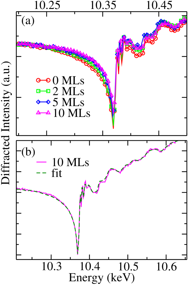
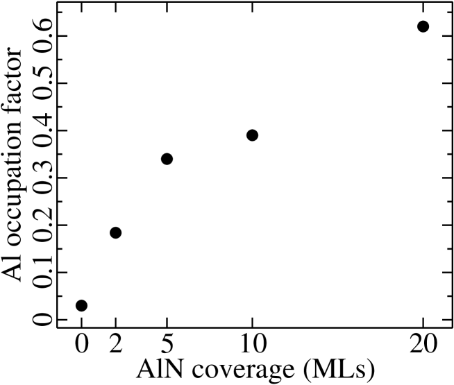
On the other side, the analysis of the DAFS edge shape can give information about the capping mechanism of the QDs. Indeed, as a first approximation, the diffracted intensity is proportional to the square modulus of the in-plane iso-strain region structure factor. We calculate this structure factor for an wurtzite structure to take into account the Al atoms belonging to the same iso-strain region as the Ga atoms at the QDs top. The Al concentration obtained by refining the value gives the Al atoms fraction seen by diffraction, contributing at the chosen Q-value, and determining the edge line shape. Taking into account that EDAFS analysis shows that no intermixing takes place, we cane state that we are probing the AlN capping. Figure 9a) shows the GIDAFS spectra for the 0, 2, 5 and 10 AlN MLs cap thicknesses, measured at the maximum of the partial structure factor (see section IV). The data were normalized so that the intensity at 10.2 keV is the same for all spectra. Equation 1 was fitted to each GIDAFS spectrum, using the anomalous scattering factors and of a GaN layer. A scale factor, the detector efficiency as a function of the energy and the Al occupation factor () inside the in-plane iso-strain region were refined. As an example, fig. 9(b) shows the best fit for the 10 MLs sample obtained with . It should be noted that the occupation factor is determined by the ratio , i.e. the curvature and depth of the cusp before and at the edge. The fit quality is the same for all samples. Figure 10 shows the Al concentration () as a function of the AlN cap thickness. Up to 5 MLs, the AlN contribution, that is near to zero () for free standing QDs, increases linearly, stabilizes above 5MLs, and at 10 MLs the contribution is almost the same as for the 5 MLs sample. Provided that AlN on top of the QDs is pseudomorphic to GaN for low coverages Coraux05a , the evolution of the Al concentration () in the iso-strain region up to 5 MLs indicates a linear increase of the amount of AlN on top of the GaN QDs. This could result from a uniform growth of AlN on the whole surface, i.e. the QDs and the thin pseudomorphic wetting layer Gogneau04 . The further evolution of the Al concentration above 5 MLs points out a change in the AlN growth process, leading to AlN with an in-plane strain state different from that in the QDs. This change may correspond either to plastic relaxation in AlN, or to selective AlN growth in between of the QDs where the stress differs from that on top of the QDs, or to another still unknown process.
VII Conclusion
We have presented new results on the structural properties of GaN QDs by combining different aspects of X-ray diffraction : quasi surface sensitivity due to grazing incidence, quantitative analysis of anomalous effect according to MAD principles, lineshape fit of DAFS and EDAFS oscillations fit.
All these aspects are strongly complementary. We determine in-plane and out-of-plane lattice parameters and investigate the effect of capping layer by monitoring its effect on the QDs strain. In addition, the Al fraction seen by the anomalous diffraction as a function of the capping layer thickness (obtained by the GIDAFS lineshape analysis at the Ga K-edge), indicates a wetting of the QDs, followed by a noticeable change in the capping process which may be related either to plastic relaxation in AlN, or to spatially selective AlN growth, or to a still unknown process. Let us point out that the Al fraction obtained in this way does not represent the Al content inside the dots, but the AlN contribution to the diffuse scattering at the same Q value as the GaN QDs contribution, i.e. AlN mostly located on top of the QDs. The Al content of the dots can be found by analysis of the EDAFS oscillations which provide the microscopic local environment of the Ga resonant atom. Our analysis shows that no Ga/Al intermixing takes place, as expected for these two group III-N elements. We recovered the in-plane and perpendicular strains and in the dots and compare them to the biaxial elastic strain of a pseudomorphic layer. We find a tendency to an over-strained regime that suggests a more complex mechanism of strain accomodation which deserves further investigations.
We are very grateful to N. Boudet, S. Arnaud, B. Caillot and J.F. Brar for help to set-up the GIDAFS experiment at beamline BM2 at the ESRF. We are very grateful to P. Wolfers who gave us the DPU code used for data analysis. The authors would like to thank C. Priester for her critical reading of the manuscript. MGP acknowledges the support of the Spanish Ministry of Education and Science in the frame of ”Programa de estancias de profesores espaoles en centros de investigacin extranjeros” (project n. PR2005-0231).
References
- [1] F. A. Ponce and D. P. Bour. Nitride-based semiconductors for blue and green light-emitting devices. Nature, 386:351, 1997.
- [2] X. H. Wu, P. Fini, E. J. Tarsa, B. Heying, S. Keller, U. K. Mishra, S. P. DenBaars, and J. S. Speck. Dislocation generation in GaN heteroepitaxy. Journal Of Crystal Growth, 189/190:231, 1998.
- [3] Y. Arakawa and H. Sakaki. Multidimensional quantum well laser and temperature dependence of its threshold current. Applied Physics Letters, 40(11):939, 1982.
- [4] N. Ledentsov, D. Bimberg, Z.. I. Alferov V. M. Ustinov, and J. A. Lott. Quantum dots for VCSEL applications at . Physica E, 13:871, 2002.
- [5] B. Daudin, F. Widmann, G. Feuillet, Y. Samson, M. Arlery, and J. L. Rouvire. Stranski-krastanov growth mode during the molecular beam epitaxy of highly strained GaN. Physical Review B, 56:R7069, 1997.
- [6] C. Adelmann, B. Daudin, R. A. Olivier, G. A. D. Briggs, and R. E. Rudd. Nucleation and growth of GaN/AlN quantum dots. Physical Review B, 70:125427, 2004.
- [7] J. Brown, F. Wu, P. M. Petroff, and J. S. Speck. GaN quantum dot density control by rf-plasma molecular beam epitaxy. Applied Physics Letters, 84(5):690, 2004.
- [8] N. Gogneau, D. Jalabert, E. Monroy, T. Shibata, M. Tanaka, and B. Daudin. Structure of GaN quantum dots grown under ”modified stranski-krastanow” conditions on AlN. Journal of Applied Physics, 94(4):2254, 2003.
- [9] C. Adelmann, N. Gogneau, E. Saragiannidou, J.-L. Rouvire, and B. Daudin. GaN islanding by spontaneous rearrangement of a strained two-dimensional layer on (0001) AlN. Applied Physics Letters, 81(16):3064, 2002.
- [10] B. Damilano, N. Grandjean, S. Dalmasso, and J. Massies. Room-temperature blue-green emission from InGaN/GaN quantum dots made by strain-induced islanding growth. Applied Physics Letters, 75(24):3751, 1999.
- [11] J. Tersoff, C. Teichert, and M. G. Lagally. Self-organization in growth of quantum dot superlattices. Physical Review Letters, 76(10):1675, 1996.
- [12] V. Chamard, T. H. Metzger, M. Sztucki, V. Holy, M. Tolan, E. Bellet-Amalric, C. Adelmann, B. Daudin, and H. Mariette. On the driving forces for the vertical alignment in nitride quantum dot multilayers. Europhysics Letters, 63:268, 2003.
- [13] J. Coraux, H. Renevier, V. Favre-Nicolin, G. Renaud, and B. Daudin. In situ resonant x-ray study of vertical correlation and capping effects during GaN/AlN quantum dots growth. http://arxiv.org/abs/cond-mat/0508126, 2005. submitted to Applied Physics Letters.
- [14] B. Daudin, J.-L. Rouvire, D. Jalabert, J. Coraux, H. Renevier, C. Mann-Ho, C. Kwun-Bum, D. W. Moon, M. G Proietti, J. M. Llorens, N. Garro, A. Cros, and A. Garca-Cristbal. Structural properties of gan quantum dots. submitted to Oxford J. Microscopy, 2005.
- [15] J. Stangl, V. Holy, and G. Bauer. Structural properties of self-organized semiconductor nanostructures. Reviews of Modern Physics, 76:725, 2004.
- [16] J.-L. Hodeau, V. Favre-Nicolin, S. Bos, H. Renevier, E. Lorenzo, and J.-F. Brar. Resonant diffraction. Chemical Reviews, 101(6):1843, 2001.
- [17] W. A. Hendrickson. Determination of macromolecular structures from anomalous diffraction of synchrotron radiation. Science, 254(5028):51, 1991.
- [18] H. Stragier, J. O. Cross, J. J. Rehr, Larry B. Sorensen, C. E. Bouldin, and J. C. Woicik. Diffraction anomalous fine structure: A new x-ray structural technique. Phyical Review Letters, 69(21):3064, 1992.
- [19] A. Letoublon, V. Favre-Nicolin, H. Renevier, M. G. Proietti, C. Monat, M. Gendry, O. Marty, and C. Priester. Strain, size, and composition of InAs quantum sticks embedded in InP determined via grazing incidence x-ray anomalous diffraction. Physical Review Letters, 92(18):186101, 2004.
- [20] T. Shibata, K. Asai, S. Sumiya, M. Mouri, M. Tanaka, O. Oda, H. Katsukawa, H. Miyake, and K. Hiramatsu. High-quality AlN epitaxial films on (0001)-faced sapphire and 6H-SiC substrate. Physica Status Solidi (C), 0(7):2023, 2003.
- [21] U. Pietsch, V. Holy, and T. Baumbach. High-resolution X-ray scattering : from thin films to lateral nanostructures. Springer Verlag, 2004.
- [22] M. Schmidbauer, D. Grigoriev, M. Hanke, P. Schafer, T. Wiebach, and R. Kohler. Effects of grazing incidence conditions on the x-ray diffuse scattering from self-assembled nanoscale islands. Physical Review B, 71:115324, 2005.
- [23] V. Favre-Nicolin. NanoMAD. Private communication, 2005.
- [24] M. G. Proietti, H. Renevier, J. L. Hodeau, J. Garcia, J. F. Berar, and P. Wolfers. Diffraction-anomalous-fine-structure spectroscopy applied to the study of III-V strained semiconductors. Physical Review B, 59:5479, 1999.
- [25] H. Renevier, S. Grenier, S. Arnaud, J. F. Brar, B. Caillot, J. L. Hodeau, A. Ltoublon, M. G. Proietti, and B. Ravel. Diffraction anomalous fine structure spectroscopy at the beam line BM2-D2AM at the European Synchrotron Radiation Facility. Journal of Synchrotron Radiation, 10:435, 2003.
- [26] A. L. Ankudinov, B. Ravel, J. J. Rehr, and S. D. Conradson. Real-space multiple-scattering calculation and interpretation of x-ray-absorption near-edge structure. Physical Review B, 58:7565, 1998.
- [27] M. Newville, B. Ravel, D. Haskel, J. J. Rehr, E. A. Stern, and Y. Yacobi. Analysis of multiple-scattering XAFS data using theoretical standards. Physica B, 208-209:154, 1995.
- [28] F. Romanato, D. De Salvador, M. Berti, A. Drigo, M. Natali, M. Tormen, G. Rossetto, S. Pascarelli, F. Boscherini, C. Lamberti, and S. Mobilio. Bond-length variation in InxGa1-xAs/InP strained epitaxial layers. Physical Review B, 57:14619, 1998.
- [29] H. Schulz and K. H. Thiemann. Crystal structure refinement of GaN and AlN. Solid State Communications, 23:815, 1997.
- [30] A. D. Andreev and E. P. O’Reilly. Theory of the electronic structure of GaN/AlN hexagonal quantum dots. Physical Review B, 62:15851, 2000.
- [31] F. d’Acapito, F. Boscherini, S. Mobilio, A. Rizzi, and R. Lantier. Epitaxy and strain in the growth of GaN on AlN: A polarized x-ray absorption spectroscopy study. Physical Review B, 66:205411, 2002.
- [32] M. Arlery, J. L. Rouvire, F. Widmann, B. Daudin, G. Feuillet, and H. Mariette. Quantitative characterization of GaN quantum-dot structures in AlN by high-resolution transmission electron microscopy. Applied Physics Letters, 74(22):3287, 1999.
- [33] N. Gogneau, E. Monroy, D. Jalabert, E. Sarigiannadou, J.-L. Rouvire, and B. Daudin. Influence of AlN overgrowth on structural properties of GaN quantum wells and quantum dots grown by plasma-assisted molecular beam epitaxy. Journal of Applied Physics, 96(2):1104, 2004.
- [34] A. Bourret, C. Adelmann, B. Daudin, J.-L. Rouviere, G. Feuillet, and G. Mula. Strain relaxation in (0001) AlN/GaN heterostructures. Physical Review B, 63:245307, 2001.
Figure Captions
Fig. 1 : AFM image of uncapped GaN QDs grown in the modified SK mode.
Fig. 2 : Grazing incidence geometry for a in-plane reflection . See text for details.
Fig. 3 : (a,c,e) : measured at 10.317 keV (50 eV below Ga K-edge), and extracted for a 0 MLs (a), a 5 MLs (c), and a 10 MLs (e) AlN coverage. (b,d,f) : Experimental square root intensities measured below (-100 and -50 eV), at (edge), and above (+ 5eV) the Ga K-edge for a 0 MLs (b), a 5 MLs (d), and a 10 MLs (f) AlN coverage.
Fig. 4: Schematic representation in the complex plane of the structure factor as a function of , and (see text). represents the partial structure factor of non resonant atoms (Al, N).
Fig. 5 : In-plane lattice parameter and strain (relative to bulk GaN) in GaN deduced from the position of the maximum. Bulk GaN gives with while bulk AlN gives with .
Fig. 6 : (a) Experimental EDAFS for the free standing QDs sample, compared with the best fit result, (b) R-space experimental curve for free standing QDs compared with best fit.
Fig. 7 : Scheme of GaN wurzite structure, the most relevant virtual phoelectron scattering paths used for the EDAFS simulation are represented : (1) in-plane I shell , (2) out-of-plane I shell , (3) out-of-plane II shell , (4) III shell Ga-N along c, (5) nearly in-plane IV shell Ga-N, MS Ga-N-N and Ga-N-Ga. Ga atoms are represented by white spheres, N by black ones.
Fig. 8 : GaN QDs strain versus values for all the samples studied compared with elastic biaxial strain of a pseudomorphic GaN thin film.
Fig. 9 : (a) GIDAFS spectra for 0, 2, 5 and 10 MLs AlN capping, measured at maximum of ; (b) crystallographic best fit for the 10 ML AlN sample, open circle : experiment, solid line : simulation performed with experimental and of a GaN thin film.
Fig. 10 : Al atoms occupation factor, , of the iso-strain region selected by diffraction (maximum of ), as a function of AlN coverage.
Table caption
Table 1 : EDAFS best fit values for interatomic distances (R), Debye-Waller factors () and Al concentration () obtained by IFEFIT mimimization using theoretical fitting standards provided by FEFF8 code. The amplitude and phase correction factors have been obtained by crystallographic analysis of the DAFS lineshape. The value is kept fixed to the value determined by grazing incidence and exit diffraction (diff.).
| Bulk | GaN/AlN | 0 MLs | 2 MLs | 5 MLs | 10 MLs | |
| R1(Ga-N) () | - | - | 1.93 | 1.94 | 1.94 | 194 |
| - | - | |||||
| R2 (Ga-Ga) () | 3.188 | 3.11 | 3.156 (diff.) | 3.147 (diff.) | 3.149 (diff.) | 3.14 (diff.) |
| - | - | |||||
| R2 (Ga-Ga) () | 3.18 | - | 3.19 | 3.18 | 3.18 | 3.19 |
| ) | 5.186 | 5.26 | 5.25 | 5.23 | 5.22 | 5.25 |
| 1.626 | 1.69 | 1.66 | 1.66 | 1.66 | 1.67 | |
| - | - | 0.1 | 0.0 | 0.1 | 0.05 |