Thermal properties in mesoscopics: physics and applications from thermometry to refrigeration
Abstract
This review presents an overview of the thermal properties of mesoscopic structures. The discussion is based on the concept of electron energy distribution, and, in particular, on controlling and probing it. The temperature of an electron gas is determined by this distribution: refrigeration is equivalent to narrowing it, and thermometry is probing its convolution with a function characterizing the measuring device. Temperature exists, strictly speaking, only in quasiequilibrium in which the distribution follows the Fermi-Dirac form. Interesting nonequilibrium deviations can occur due to slow relaxation rates of the electrons, e.g., among themselves or with lattice phonons. Observation and applications of nonequilibrium phenomena are also discussed. The focus in this paper is at low temperatures, primarily below 4 K, where physical phenomena on mesoscopic scales and hybrid combinations of various types of materials, e.g., superconductors, normal metals, insulators, and doped semiconductors, open up a rich variety of device concepts. This review starts with an introduction to theoretical concepts and experimental results on thermal properties of mesoscopic structures. Then thermometry and refrigeration are examined with an emphasis on experiments. An immediate application of solid-state refrigeration and thermometry is in ultrasensitive radiation detection, which is discussed in depth. This review concludes with a summary of pertinent fabrication methods of presented devices.
I Introduction
Solid state mesoscopic electronic systems provide a micro-laboratory to realize experiments on low temperature physics, to study quantum phenomena such as fundamental relaxation mechanisms in solids, and a way to create advanced cryogenic devices. In a broad sense, mesoscopic here refers to micro- and nanostructures, whose size falls in between atomic and macroscopic scales. The central concept of this Review is the energy distribution of mesoscopic electron systems, which in thermal equilibrium (Fermi-Dirac distribution) determines the temperature of the electron gas. The non-Fermi distributions are discussed in depth, since they are often encountered and utilized in mesoscopic structures and devices. This Review aims to discuss the progress mainly during the past decade on how electron distributions can be controlled, measured and made use of in various device concepts. When appropriate, earlier developments are reviewed as well. The central devices and concepts to be discussed are electronic refrigerators, thermometers, radiation detectors, and distribution-controlled transistors. Typically the working principles or resolution of these detectors rely on phenomena that show up only at cryogenic temperatures, i.e., at temperatures of the order of a few kelvin and below. A practical threshold in terms of temperature is set by liquefaction of helium at 4.2 K. This also sets the emphasis in this Review: the devices and principles working mostly at temperatures above 4.2 K are at times mentioned only for reference.
Section II of this Review introduces formally the central ingredients; the relevant theoretical results are either derived or given there. We also review some of the new developments concerning the thermoelectric effects in mesoscopic systems. Although the theoretical analysis of the effects in the later sections is based on Sec. II, the main messages can be understood without reading it in detail. Section III explains how the electronic temperature is typically measured and what is required of an electronic thermometer. Accurate and fast thermometers can be utilized for thermal radiation detection as explained in Sec. IV, which reviews such detectors. The resolution of these devices is ultimately limited by the thermal noise, which can be lowered by refrigeration. In Sec. V, we show how the electron temperature can be lowered via electronic means, and discuss the direct applications of this refrigeration. Section VI explains the main methods used in the fabrication of mesoscopic electronic devices, and in Sec. VII we briefly discuss some of the main open questions in the field and the prospects of practical instruments based on electronic refrigeration and using the peculiar out-of-equilibrium energy distributions.

II Thermal properties of mesoscopic scale hybrid structures at sub-kelvin temperatures
The schematic picture of a setup studied in typical experiments described in this Review is shown in Fig. 1. The main object is a diffusive metal or heavily-doped semiconductor wire connected to large electrodes acting as reservoirs where electrons thermalize quickly to the surroundings. The electrons in the wire interact between themselves, and are coupled to the phonons in the film and to the radiation and the fluctuations in the electromagnetic environment. The temperature of the film phonons can, in a non-equilibrium situation, differ from that of the substrate phonons, and this can even differ from the phonon temperature in the sample holder that is externally cooled. Under the applied voltage, the energy distribution function of electrons depends on each of these couplings, and on the state (e.g., superconducting or normal) of the various parts of the system. In certain cases detailed below, is a Fermi function
| (1) |
characterized by an electron temperature and potential . One of the main goals of this review is to explain how , and in some cases also , can be driven even much below the lattice temperature , and how this low can be exploited to improve the sensitivity of applications relying on the electronic degrees of freedom. We also detail some of the out-of-equilibrium effects, where is not of the form of Eq. (1). In some setups, the specific form of can be utilized for novel physical phenomena.
Throughout the Review, we concentrate on wires whose dimensions are large enough to fall in the quasiclassical diffusive limit. This means that the Fermi wavelength , elastic mean free path and the length of the wire have to satisfy . In this regime, the electron energy distribution function is well defined, and its space dependence can be described by a diffusion equation (Eq. (3)). In most parts of the Review, we assume the capacitances of the contacts large enough, such that the charging energy is less than any of the relevant energy scales and can thus be ignored.
Our approach is to describe the electron energy distribution function at a given position of the sample and then relate this function to the charge and heat currents and their noise. In typical metal structures in the absence of superconductivity, phase-coherent effects are weak and often it is enough to rely on a semiclassical description. In this case, is described by a diffusion equation, as discussed in Subs. II.1. The electron reservoirs impose boundary conditions for the distribution functions, specified in Subs. II.2. The presence of inelastic scattering due to electron-electron interaction, phonons or the electromagnetic environment can be described by source and sink terms in the diffusion equation, specified by the collision integrals and discussed in Subs. II.3. In the limit when these scattering effects are strong, the distribution function tends to a Fermi function throughout the wire, with a position dependent potential and temperature . In this quasiequilibrium case, detailed in Subs. II.4, it thus suffices to find these two quantities. Finally, with the knowledge of , one can obtain the observable currents and their noise as described in Subs. II.5.
In many cases, it is not enough to only describe the electrons inside the mesoscopic wire, assuming that the surroundings are totally unaffected by the changes in this electron system. If the phonons in the film are not well coupled to a large phonon bath, their temperature is influenced by the coupling to the electrons. In this case, it is important to describe the phonon heating or cooling in detail (see Subs. II.7). Often also the electron reservoirs may get heated due to an applied bias voltage, which has to be taken into account in the boundary conditions. This heating is discussed in Subs. II.8.
At the temperature range considered in this Review, many metals undergo a transition to the superconducting state Tinkham (1996). This gives rise to several new phenomena that can be exploited, for example, for thermometry (see Sec. III), for radiation detection (Sec. IV) and for electron cooling (Sec. V). The presence of superconductivity modifies both the diffusion equation (inside normal-metal wires through the proximity effect, see Subs. II.1) and especially the boundary conditions (Subs. II.2). Also the relations between the observable currents and the distribution functions are modified (Subs. II.5).
Once the basic equations for finding are outlined, we detail its behavior in different types of normal-metal – superconductor heterostructures in Subs. II.6.
II.1 Boltzmann equation in a diffusive wire
The semiclassical Boltzmann equation Ashcroft and Mermin (1976); Smith and Jensen (1989) describes the average number of particles, , in the element around the point in the six-dimensional position-momentum space. The kinetic equation for is a continuity equation for particle flow,
| (2) |
Here is the electric field driving the charged particles and the elastic and inelastic collision integrals and , functionals of , act as source and sink terms. They illustrate the fact that scattering breaks translation symmetries in space and time — the total particle numbers expressed through the momentum integrals of still remain conserved.
In the metallic diffusive limit, Eq. (2) may be simplified as follows Nagaev (1992); Sukhorukov and Loss (1999); Rammer (1998). The electric field term can be absorbed in the space derivative by the substitution in the argument of the distribution function, such that describes both the kinetic and the potential energy of the electron. Therefore, we are only left with the full -dependent derivative on the left-hand side of Eq. (2). In the diffusive regime, one may concentrate on length scales much larger than the mean free path . There, the particles quickly lose the memory of the direction of their initial momentum, and the distribution functions become nearly isotropic in the direction of . Therefore, we may expand the distribution function in the two lowest spherical harmonics in the dependence on , , and make the relaxation-time approximation to the elastic collision integral with the elastic scattering time , i.e., . In the limit where the time dependence of the distribution function takes place in a much slower scale than , this yields the diffusion equation with a source term,
| (3) |
Here we assume that the particles move with the Fermi velocity, i.e., . As a result, their diffusive motion is characterized by the diffusion constant . In what follows, we will mainly concentrate on the static limit, i.e., assume and lift the subscript 0 from the angle-independent part of the distribution function.
Equation (3) can also be derived rigorously from the microscopic theory through the use of the quasiclassical Keldysh formalism Rammer and Smith (1986). With such an approach, one can also take into account superconducting effects, such as Andreev reflection Andreev (1964b) and the proximity effect Belzig et al. (1999). In the diffusive limit, one obtains the Usadel equation Usadel (1970), which in the static case is
| (4) |
Here is the isotropic part of the Keldysh Green’s function in the Keldysh Nambu space, and are the cross section and the normal-state conductivity of the wire, is the third Pauli matrix in Nambu space, is the pair potential matrix, and describes the inelastic scattering that is not contained in . Usadel equation describes the matrix current Nazarov (1999), whose components integrated over the energy yield the physical currents. In the Keldysh space, is of the form
where each component is a matrix in Nambu particle-hole space. Equation (4) has to be augmented with a normalization condition . This implies and allows a parametrization , where is a distribution function matrix with two free parameters. The equations for the retarded/advanced functions ((1,1) and (2,2) -Keldysh components of Eq. (4)) describe the behavior of the pairing amplitude. The solutions to these equations yield the coefficients for the kinetic equations, i.e., the (1,2) or the Keldysh part of Eq. (4). This describes the symmetric and antisymmetric parts of the energy distribution function with respect to the chemical potential of the superconductors. The latter is assumed everywhere equal to allow a time-independent description. A common choice is a diagonal Schmid and Schön (1975), where is the antisymmetric and the symmetric part of the energy distribution function . With this choice, inside the normal metals where , we get two kinetic equations of the form Belzig et al. (1999); Virtanen and Heikkilä (2004a)
| (5a) | |||||
| (5b) | |||||
Here describes the spectral energy current, and the spectral charge current. The inelastic effects are described by the collision integrals and . The kinetic coefficients are
Here, and are the spectral energy and charge diffusion coefficients, and is the spectral density of the supercurrent-carrying states Heikkilä et al. (2002). The cross-term is usually small but not completely negligible. In a normal-metal wire in the absence of a proximity effect, and . Then we obtain , and the kinetic equations (5b) reduce to Eq. (3) in the static limit.
II.2 Boundary conditions
The quasiclassical kinetic equations cannot directly describe constrictions whose size is of the order of the Fermi wavelength, such as tunnel junctions or quantum point contacts. However, such contacts can be described by the boundary conditions derived by Nazarov (1999),
| (6) |
where
Here, , and and are the matrix current and the Green’s function at the left (right) of the constriction, evaluated at the interface and flowing towards the right. The constriction is described by a set of transmission eigenvalues through the function . For large constrictions, it is typically enough to transform the sum over the eigenvalues to an integral over the transmission probabilities , weighted by their probability distribution . In the case of a tunnel barrier, , and thus . For a ballistic contact and . For other types of contacts, it is typically useful to find the observable for arbitrary and weight it with , e.g., for a diffusive contact Nazarov (1994), for a dirty interface Schep and Bauer (1997) or for a chaotic cavity Baranger and Mello (1994). This way, the observables can be related to the normal-state conductance of the junction.
Equation (6) yields a boundary condition both for the ”spectral” functions and for the distribution functions. In the absence of superconductivity, we simply have , and the boundary condition for the distribution functions becomes independent of the type of the constriction,
| (7) |
In this case, the two currents can be included in the same function by defining . This yields the spectral current through the constriction
| (8) |
where is the energy distribution function on the left/right side of the constriction.
Another interesting yet tractable case is the one where a superconducting reservoir (on the ”left” of the junction) is connected to a normal metal (on the ”right”) and the proximity effect into the latter can be ignored. The latter is true, for example, if we are interested in the distribution function at energies far exceeding the Thouless energy of the normal-metal wire, or in the presence of strong depairing. In this case, the spectral energy and charge currents are
| (9a) | ||||
| (9b) | ||||
Here and is the Heaviside step function, and the energy-dependent coefficients are
| (10a) | ||||
| (10b) | ||||
| (10c) | ||||
Here we defined . In the tunneling limit , we get
| (11) |
where
| (12) |
is the reduced superconducting density of states (DOS). The first form of Eq. (12) assumes a finite pair-breaking rate , which turns out to be relevant in some cases discussed in Sec. V.C.1 Unless specified otherwise, we assume that the superconductors are of the conventional weak-coupling type and the superconducting energy gap at is related to the critical temperature by Tinkham (1996).
II.3 Collision integrals for inelastic scattering
The collision integral in Eq. (3) is due to electron–electron, electron–phonon interaction and the interaction with the photons in the electromagnetic environment.
II.3.1 Electron-electron scattering
For the electron–electron interaction, the collision integral is of the form
| (13) |
where and depend on the type of scattering and the ”in” and ”out” collisions are
| (14a) | ||||
| (14b) | ||||
Electron-electron scattering can be either due to the direct Coulomb interaction Altshuler and Aronov (1985), or mediated through magnetic impurities which can flip their spin in a scattering process Kaminski and Glazman (2001) or other types of impurities with internal dynamics. In practice, both of these effects contribute to the energy relaxation Anthore et al. (2003); Pierre et al. (2000). Assuming the electron–electron interaction is local on the scale of the variations in the distribution function, the direct interaction yields Altshuler and Aronov (1985) Eq. (13) with for a -dimensional wire. In a diffusive wire, the effective dimensionality of the wire is determined by comparing the dimensions to the energy-dependent length . The prefactor for a -dimensional sample is
| (15a) | ||||
| (15b) | ||||
| (15c) | ||||
where is the density of states at the Fermi energy and is the wire cross-section.
In the case of relaxation due to magnetic impurities, one expects Kaminski and Glazman (2001) and . Here is the concentration, is the spin, and is the Kondo temperature of the magnetic impurities responsible for the scattering. This form is valid for . For a more detailed account of the magnetic-impurity effects, see Göppert and Grabert (2001, 2003); Göppert et al. (2002); Kroha and Zawadowski (2002); Ujsaghy et al. (2004) and the references therein.
For , and for small deviations from equilibrium, the collision integral can be approximated Rammer (1998) by , where is the relaxation time (), is the elastic scattering time and is the Fermi momentum. In the case when , the usual relaxation-time approach does not work for the electron–electron interaction as the expression for the relaxation time has an infrared divergence Altshuler and Aronov (1985); Rammer (1998). Therefore, one has to solve the full Boltzmann equation with the proper collision integrals. To obtain an estimate for the length scale at which the electron–electron interaction is effective, we can proceed differently. Introducing dimensionless position and energy variables and , we get
Here the dimensionless integral characterizes the deviation in the shape of the distribution function from the Fermi function and depends on the specific system. For a quasi-1d wire with bare Coulomb interaction,
| (16) |
where , is the resistance of the wire and is the Thouless energy. In the case when the wire terminates in a point contact with resistance , the resistance in Eq. (16) should be replaced with the total resistance Pekola et al. (2004a). Typically the energy scale characterizing the deviation from (quasi)equilibrium is . At , electron–electron collisions start to be effective when . This yields a length scale
| (17) |
where is the cross section of the wire and its conductivity. Using a wire with resistance and eV for m (close to the values in Huard et al. (2004)), and a voltage V, we get m. Increasing the temperature, becomes smaller, and this effective length also decreases. The experimental results of Huard et al. (2004) indicate at least an order of magnitude larger and thus smaller than predicted by this theory. At present, the reasons for this discrepancy have not been found.
II.3.2 Electron–phonon scattering
Another source of inelastic scattering is due to phonons, for which the collision integral is of the form Rammer (1998); Wellstood et al. (1994)
| (18) |
Here
| (19) |
The kernel (the Eliashberg function) of the interaction depends on the type of considered phonons (longitudinal or transverse), on the relation between the phonon wavelength and the electron mean free path , on the dimensionality of the electron and phonon system Sergeev et al. (2005), and on the characteristics of the Fermi surface Prunnila et al. (2005). At sub-kelvin temperatures and low voltages, the optical phonons can be neglected, and one can only concentrate on the acoustic phonons. In what follows, we also neglect phonon quantization effects which may be important in restricted geometries. Moreover, the phonon distribution function is considered to be in (quasi)equilibrium, i.e., described by a Bose distribution function (for phonon relaxation processes, see Subs. II.7).
When the phonon temperature is much lower than the Debye temperature , the phonon dispersion relation is linear and one can estimate the phonon wavelength using . For typical metals, the speed of sound is km/s, which yields a wavelength nm at K and m at mK. In the clean limit , approximating the electron-phonon coupling with a scalar deformation potential, only the longitudinal phonons are coupled to the electrons. In this case for Wellstood et al. (1994); Rammer (1998)
| (20) |
where is the square of the matrix element for the deformation potential. Generally this is inversely proportional to the mass density of the ions, but its precise microscopic form depends on the details of the lattice structure. Therefore it is useful to present in terms of a separately measurable quantity, e.g., the prefactor of the power dissipated to the lattice of volume in the quasiequilibrium limit (see Table 1 and Subs. II.4): , where .
| (mK) | (mK) | (W m-3K | Measured in | |
| Ag | 50…400 | 50…400 | 0.5 109 | Steinbach et al. (1996) |
| Al | 35…130 | 35 | 0.2 109 | Kautz et al. (1993) |
| 200…300 | 200 | 0.3 109 | Meschke et al. (2004) | |
| Au | 80…1200 | 80…1000 | 2.4 109 | Echternach et al. (1992) |
| AuCu | 50…120 | 20…120 | 2.4 109 | Wellstood et al. (1989) |
| Cu | 25…800 | 25…320 | 2.0 109 | Roukes et al. (1985) |
| 100…500 | 280…400 | 0.9…4 109 | Leivo et al. (1996) | |
| 50…200 | 50…150 | 2.0 109 | Meschke et al. (2004) | |
| Mo | 980 | 80…980 | 0.9 109 | Savin and Pekola (2005) |
| n++Si | 120…400 | 175…400 | 0.1 109 | Savin et al. (2001) |
| 173…450 | 173 | 0.04 109 | Prunnila et al. (2002) | |
| 320…410 | 320…410 | 0.1 109 | Buonomo et al. (2003) | |
| Ti | 300…800 | 500…800 | 1.3 109 | Manninen et al. (1999) |
In the dirty limit , the power of in the Eliashberg function can be either 1 or 3, for the cases of static or vibrating disorder, respectively. For further details about the dirty limit, we refer to Belitz (1987); Sergeev and Mitin (2000); Rammer and Schmid (1986).
The relaxation rate for electron-phonon scattering is given by , where now is a Fermi function at the lattice temperature. With this definition at , Rammer (1998)
| (21) |
Thus, in the clean case for we obtain , . With typical values for Cu, and J-1m-3, we get ns at K. Assuming , the electron–phonon scattering length is . For the above values and a typical diffusion constant m2/s, m at K and m at mK.
In the disordered limit , the temperature dependence of the electron-phonon scattering rate is expected to follow either the or laws, depending on the nature of the disorder Sergeev and Mitin (2000).
It seems that although most of the experiments are done in the limit where the phonon wavelength at least slightly exceeds the electron mean free path, in majority of the cases the results have fitted to the clean-limit expressions, i.e., the scattering rate and the heat current flowing into the phonon system , see Eq. (24) below (for an exception, see Karvonen et al. (2005)). Finding the correct exponent is not straightforward, as the film phonons are also typically affected by the measurement, and because of the reduced dimensionality of the phonon system (see Subs. II.7). In this Review, we concentrate on the clean-limit expressions.
II.4 Quasiequilibrium limit
The shape of the distribution function at a given position of the wire strongly depends on how the inelastic scattering length compares to the length of the wire. For (nonequilibrium limit), we may neglect the inelastic scattering altogether. In this case, the distribution function is a solution to either Eqs. (5) or Eq. (3), where the collision integrals/self energies for inelastic scattering can be neglected. As a result, the shape of the electron distribution functions inside the wire at a finite bias voltage may strongly deviate from a Fermi distribution Pothier et al. (1997b); Pierre et al. (2001); Heslinga and Klapwijk (1993); Heikkilä et al. (2003); Pekola et al. (2004a); Giazotto et al. (2004b). The nonequilibrium shape shows up in most of the observable properties of the system, including the characteristics, the current noise or the supercurrent. In general, it can only be neglected in the characteristics if the charge transport process is energy independent as in the case of purely normal-metal samples. Even in this case the form of can be observed in the current noise.
The kinetic equations can be greatly simplified in the limit where for one type of scattering is much smaller than . In the quasiequilibrium limit, the energy relaxation length due to electron–electron scattering is much shorter than the wire, Nagaev (1995). In this case, the local distribution function is a Fermi function characterized by the temperature and potential . Mathematically, this can be seen by considering the Boltzmann equation (3) with the electron–electron collision integral, Eq. (13) in the limit where the prefactor of the latter becomes very large. As the left-hand side of Eq. (3) is not strongly dependent on the form of as a function of energy, the equation can only be satisfied if the collision integral without the prefactor becomes small. It can be easily shown that the latter vanishes for . Thus, the deviations from the Fermi-function shape will be at most of the order of , and can be neglected in the quasiequilibrium limit.
In this limit, we are still left with two unknowns, and . Substituting in Eq. (3) yields
where contains the other types of inelastic scatterings, e.g., those with the phonons. In the right hand side of the upper line, the differential operators and act only on and . Integrating this over the energy and multiplying by and then integrating over yields
| (22) | ||||
| (23) |
We assumed that the energy integral over vanishes.111In the diffusive limit where the inelastic scattering rates are lower than , this is related to the particle number conservation and is thus generally valid. Here is the electron heat capacity, is the Drude conductivity, is the electron heat conductivity, is the Lorenz number and contains the power per unit volume emitted or absorbed by other excitations, such as phonons or the electromagnetic radiation field. The last term on the left hand side of Eq. (23) describes the Joule heating due to the applied voltage. In what follows, we write the volume explicitly in the collision integral by averaging over a small volume around the point where is approximately constant, thus defining .
For the electron-phonon scattering Wellstood et al. (1994), reads in the clean case (see also Table 1)
| (24) |
For the dirty limit specified below Eq. (20), the Eliashberg functions scaling with translate into temperature dependences scaling as , i.e., and Sergeev and Mitin (2000).
The electrons can also be heated due to the thermal noise in their electromagnetic environment unless proper filtering is realized to prevent this heating. If one aims to detect the electromagnetic environment as discussed in Sec. IV, this discussion can of course be turned around to find the optimal coupling to the radiation to be observed. A model for such coupling in the quasiequilibrium limit was considered by Schmidt et al. (2004a), who obtained an expression for the emitted/absorbed power due to the external noise in the form
| (25) |
Here is the coupling constant, is the (noise) temperature of the environment, and and are the resistances characterizing the thermal noise in the electron system and the environment, respectively. This expression assumes a frequency independent environment in the relevant frequency range. For some examples on the frequency dependence, we refer to Schmidt et al. (2004a).
II.5 Observables
II.5.1 Currents
In the nonequilibrium diffusive limit, the charge current in a normal-metal wire in the absence of a proximity effect or any such interference effects as weak localization is obtained from the local distribution function by
| (26) |
and the heat current from a reservoir with potential is
| (27) |
Here we included the possible energy dependence of the diffusion constant and of the density of states , due to the energy dependence of the elastic scattering time, or due to the nonlinearities in the quasiparticle dispersion relation. If the Kondo effect Vavilov et al. (2003) can be neglected, such effects are very small in good metals at temperatures of the order of 1 K or less.
When a diffusive wire of resistance is connected to a reservoir through a point contact characterized by the transmission eigenvalues , the final distribution function is obtained after solving the Boltzmann equation (3) or Eqs. (5) with the boundary conditions given by Eq. (6), (8), or by (9). However, when is much less than the normal-state resistance of the contact, we can ignore the wire and obtain the full current by a direct integration over Eq. (8) or Eq. (9). For example, for NIS or SIS tunnel junctions, the expressions for the charge and heat currents from the left side of the junction become
| (29) | ||||
| (30) |
Here , , is the reduced density of states for the left/right wire, for a normal metal and for a superconductor. Furthermore, if the two wires constitute reservoirs, are Fermi functions with potentials , . The resulting NIS or SIS charge current is a sensitive probe of temperature and can hence be used for thermometry or radiation detection, as explained in Secs. III.1 and IV, respectively. Moreover, analysis of the heat current Eq. (30) shows that the electrons can in certain situations be cooled in NIS/SIS structures, as discussed in Sec. V.3.1.
In the presence of a proximity effect, the equations for the charge and thermal currents in the quasiclassical limit, i.e., ignoring the energy dependence of the diffusion constant and the normal-metal density of states, are
| (31a) | ||||
| (31b) | ||||
Here is the potential of the reservoir from which the heat current is calculated. As in Eq. (5), these currents can be separated into quasiparticle, anomalous, and supercurrent parts.
II.5.2 Noise
Often one can express the zero-frequency current noise in terms of the local distribution function Blanter and Büttiker (2000). The noise is characterized by the correlator
where and is the current operator. In a stationary system is independent of . In a normal-metal wire of length in the nonequilibrium limit, the current noise can be expressed as Nagaev (1992)
| (32) |
In the quasiequilibrium regime, this equation simplifies to Nagaev (1995)
| (33) |
When the resistance of a point contact dominates that of the wire, the noise power can be expressed through Blanter and Büttiker (2000)
for a normal-metal contact and de Jong and Beenakker (1994)
for an incoherent NS contact at . Here are the distribution functions in the left/right (normal/superconducting in the latter case) side of the contact and , the symmetric part w.r.t. the S potential. If the scattering probabilities are independent of energy and if the two sides are reservoirs with the same temperature, these expressions simplify to
| (34a) | ||||
| (34b) | ||||
where . For (thermal Johnson-Nyquist noise), , where and are the conductances of the point contact in the NN and NS cases, respectively. In the opposite limit (shot noise), one obtains , where is the average current through the junction, and are the Fano factors: and .
In the presence of the superconducting proximity effect, the expression for the noise becomes more complicated Houzet and Pistolesi (2004). In general, it can be found by employing the counting-field technique developed by Nazarov and coworkers, see Nazarov and Bagrets (2002) and the references therein. This technique can also be applied to study the full counting statistics of the transmitted currents through a given sample within a given measurement time Nazarov (2003).
Apart from the charge current, also the heat current in electric circuits fluctuates. For example, the zero-frequency heat current noise from the ”left” of a tunnel contact biased with voltage is given by
| (35) |
At low voltages , the heat current noise obeys the fluctuation-dissipation result , where is the thermal conductance. This quantity is related to the noise equivalent power (NEP) discussed in the literature of thermal detectors by NEP2. The total NEP contains contributions not only from the electrical heat current noise, but also from other sources, such as the direct charge current noise and electron-phonon coupling. A detailed discussion of various NEP sources is presented in Sec. IV.
Another important quantity is the cross-correlator between the current and heat current fluctuations. At zero frequency, this is given by
| (36) |
These types of fluctuations have to be taken into account for example when analyzing the NEP of bolometers Golubev and Kuzmin (2001). Recently, also the general statistics of the heat current fluctuations have been theoretically addressed by Kindermann and Pilgram (2004).
II.6 Examples on different systems
Below, we detail the solutions to the kinetic equations, (3) or (5) in some example systems. The aim is first to provide an understanding of the general behavior of the distribution function in these systems, but also to show the generic features, such as the electron cooling in NIS junctions.
II.6.1 Normal-metal wire between normal-metal reservoirs
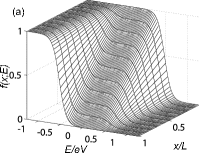
The simplest example is a quasi-one-dimensional normal-metal diffusive wire of resistance , connected to two normal-metal reservoirs by clean contacts. In the full nonequilibrium limit, we find (see Fig. 2 (a); the coordinate follows Fig. 1)
| (37) |
where and are the (Fermi) distribution functions in the left and right reservoirs with temperatures and and potentials and , respectively. The resulting two-step form illustrated in Fig. 2a was first measured by Pothier et al. (1997b).
In the quasiequilibrium limit, we get , where
| (38a) | ||||
| (38b) | ||||
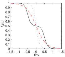
In both cases, the current is simply given by and the heat current in the limit by . For , the resistor dissipates power and is not conserved. The electron distribution function in the center of the wire, is plotted in Fig. 3 for the nonequilibrium, quasiequilibrium and local equilibrium (strong electron–phonon scattering) limits.
To obtain estimates for the thermoelectric effects due to the particle-hole symmetry breaking, let us lift the assumption of energy independent diffusion constant and density of states, expanding them as and . For linear response, the resulting expressions for the charge and heat currents are Cutler and Mott (1969)
| (39a) | ||||
| (39b) | ||||
Here is the Drude conductance, (Wiedemann-Franz law) is the heat conductance, (Mott law) is the Seebeck coefficient describing the thermoelectric power, (Onsager relation) is the Peltier coefficient, and describes effects due to the particle-hole symmetry breaking. We see that the thermoelectric effects are in general of the order ; in good metals at temperatures of the order of 1 K they can hence be typically ignored. Therefore, the Peltier refrigerators discussed in Subs. V.2 rely on materials with a low .
II.6.2 Superconducting tunnel structures
Consider a NIS tunnel structure, coupling a large superconducting reservoir with temperature to a large normal-metal reservoir with temperature via a tunnel junction with resistance . Let us then assume a voltage applied over the system. In this case, the heat current (cooling power) from the normal metal is given by Eq. (30) with , , and . For small pair breaking inside the superconductor, i.e., , is positive for , i.e., it cools the normal metal. It is straightforward to show that . This is in contrast with Peltier cooling, where the sign of the current determines the direction of the heat current. For , the current through the junction increases strongly, resulting in Joule heating and making negative. The cooling power is maximal near .
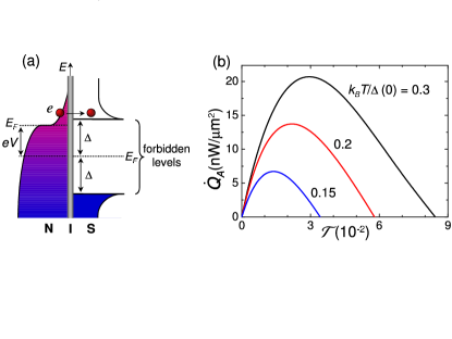
In order to understand the basic mechanism for cooling in such systems, let us consider the simplified energy band diagram of a NIS tunnel junction biased at voltage , as depicted in Fig. 4(a). The physical mechanism underlying quasiparticle cooling is rather simple: owing to the presence of the superconductor, in the tunneling process quasiparticles with energy cannot tunnel inside the forbidden energy gap, but the more energetic electrons (with ) are removed from the N electrode. As a consequence of this ”selective” tunneling of hot particles, the electron distribution function in the N region becomes sharper: the NIS junction thus behaves as an electron cooler.
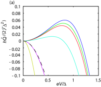
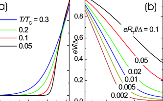
The role of barrier transmissivity in governing heat flux across the NIS structure was analyzed by Bardas and Averin (1995). They pointed out the interplay between single-particle tunneling and Andreev reflection Andreev (1964a) on the heat current. In the following it is useful to summarize their main results.
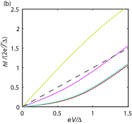
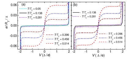
The cooling regime requires a tunnel contact. The effect of transmissivity is illustrated in Fig. 4(b), which shows the maximum of the heat current density (i.e., the specific cooling power) versus interface transmissivity at different temperatures. This can be calculated for a generic NS junction using Eqs. (9), (10a) and (31b). The quantity is a non-monotonic function of interface transmissivity, vanishing both at low and high values of . In the low transparency regime, turns out to be linear in , showing that electron transport is dominated by single particle tunneling. Upon increasing barrier transmissivity, Andreev reflection begins to dominate quasiparticle transport, thus suppressing heat current extraction from the N portion of the structure. The heat current is maximized between these two regimes at an optimal barrier transmissivity, which is temperature dependent. Furthermore, by decreasing the latter leads to a reduction of both the optimal and of the transmissivity window where the cooling takes place. In real NIS contacts used for cooling applications, the average is typically in the range Nahum et al. (1994); Leivo et al. (1996) corresponding to junction specific resistances (i.e., the product of the junction normal state resistance and the contact area) from tens to several thousands m2. This limits the achievable to some pWm2. From the above discussion it appears that exploiting low- tunnel contacts is an important requirement in order to achieve large cooling power through NIS junctions. However, in real low- barriers, pinholes with a large appear. They contribute with a large Joule heating (see Fig. 5, which shows the heat and charge currents through the NIS interface as functions of voltage for different ), and therefore tend to degrade the cooling performance at the lowest temperatures, and to overheat the superconductor at the junction region due to strong power injection. Barrier optimization in terms of both materials and technology seems to be still nowadays a challenging task (see also Sec. VI.6.1).
In a SINIS system in the quasiequilibrium limit, the temperatures and of the N and S parts may differ. If the superconductors are good reservoirs, equals the lattice temperature. In the experimentally relevant case when the resistance of the normal-metal island is much lower than the resistances and of the tunnel junctions, the normal-metal temperature is determined from the heat balance equation
| (40) |
where and describes inelastic scattering due to phonons (Eq. (24)) and/or due to the electromagnetic environment (Eq. (25)).
For further details about NIS/SINIS cooling in the quasiequilibrium limit, we refer to Sec. V.3.1 and Anghel and Pekola (2001).
Let us now consider the limit of full nonequilibrium, neglecting the proximity effect from the superconductors on the normal-metal island.222This is justified in the limit . Then the distribution function inside the normal metal may be obtained by solving the kinetic equation Eq. (3) in the static case along with the boundary conditions given by Eq. (8). For simplicity, let us assume . In this limit, the distribution function in the normal-metal island is almost independent of the spatial coordinate. Then, in Eq. (3) we can use , where is the length of the N wire. From Eq. (11) we then get
| (41) |
where is the diffusion time through the island. As a result Heslinga and Klapwijk (1993); Giazotto et al. (2004b), the distribution function in the central wire can be expressed as
| (42) |
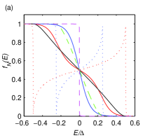
Here is the volume of the island. In the presence of inelastic scattering, this is an implicit equation, as is a functional of . Examples of the effect of inelastic scattering have been considered in Heslinga and Klapwijk (1993) in the relaxation time approach, and in Giazotto et al. (2004b) including the full electron–electron scattering collision integral. The distribution function in Eq. (42) is plotted in Fig. 6 for a few values of the voltage for and for a few strengths of electron–electron scattering at .
II.6.3 Superconductor-normal-metal structures with transparent contacts
If a superconductor is placed in a good electric contact with a normal metal, a finite pairing amplitude is induced in the normal metal within a thermal coherence length near the interface. This superconducting proximity effect modifies the properties of the normal metal Lambert and Raimondi (1998); Belzig et al. (1999) and makes it possible to transport supercurrent through it. It also changes the local distribution functions by modifying the kinetic coefficients in Eq. (5). Superconducting proximity effect is generated by Andreev reflection Andreev (1964b) at the normal-superconducting interface, where an electron scatters from the interface as a hole and vice versa. Andreev reflection forbids the sub-gap energy transport into the superconductor, and thus modifies the boundary conditions for the distribution functions. In certain cases, the proximity effect is not relevant for the physical observables whereas the Andreev reflection can still contribute. This incoherent regime is realized if one is interested in length scales much longer than the extent of the proximity effect. Below, we first study such ”pure” Andreev-reflection effects, and then go on to explain how they are modified in the presence of the proximity effect.
In the incoherent regime, for , Andreev reflection can be described through the boundary conditions Pierre et al. (2001)
| (43a) | |||
| (43b) | |||
evaluated at the normal-superconducting interface. Here is the unit vector normal to the interface and is the chemical potential of the superconductor. The former equation guarantees the absence of charge imbalance in the superconductor, while the latter describes the vanishing energy current into it. For , the usual normal-metal boundary conditions are used. Note that these boundary conditions are valid as long as the resistance of the wire by far exceeds that of the interface; in the general case, one should apply Eqs. (9).
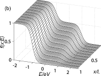
Assume now a system where a normal-metal wire is placed between normal-metal (at , potential and temperature ) and superconducting reservoirs (at , , ). Solving the Boltzmann equation (3) then yields Nagaev and Buttiker (2001)
| (44) |
Here and . This function is plotted in Fig. 2 (b). In the quasiequilibrium regime, the problem can be analytically solved in the case , i.e., when Eqs. (43) apply for all relevant energies. Then the boundary conditions are and at the NS interface. Thus, the quasiequilibrium distribution function is given by with and
| (45) |
Note that this result is independent of the temperature of the superconducting terminal.
In this incoherent regime, the electrical conductance is unmodified compared to its value when the superconductor is replaced by a normal-metal electrode: Andreev reflection effectively doubles both the length of the normal conductor and the conductance for a single transmission channel Beenakker (1992), and thus the total conductance is unmodified. Wiedemann-Franz law is violated by the Andreev reflection: there is no heat current into the superconductor at subgap energies. However, the sub-gap current induces Joule heating into the normal metal and this by far overcompensates any cooling effect from the states above (see Fig. 5).
The SNS system in the incoherent regime has also been analyzed by Bezuglyi et al. (2000) and Pierre et al. (2001). Using the boundary conditions in Eqs. (43) at both NS interfaces with different potentials of the two superconductors leads to a set of recursion equations that determine the distribution functions for each energy. The recursion is terminated for energies above the gap, where the distribution functions are connected simply to those of the superconductors. This process is called the multiple Andreev reflection: in a single coherent process, a quasiparticle with energy entering the normal-metal region from the left superconductor undergoes multiple Andreev reflections, and its energy is increased by the applied voltage during its traversal between the superconductors. Finally, when it has Andreev reflected times, its energy is increased enough to overcome the energy gap in the second superconductor. The resulting energy distribution function is a staircase pattern, and it is described in detail in Pierre et al. (2001). The width of this distribution is approximately , and it thus corresponds to extremely strong heating even at low applied voltages.
The superconducting proximity effect gives rise to two types of important contributions to the electrical and thermal properties of the metals in contact to the superconductors: it modifies the charge and energy diffusion constants in Eqs. (5), and allows for finite supercurrent to flow in the normal-metal wires.
The simplest modification due to the proximity effect is a correction to the conductance in NN’S systems, where N’ is a phase-coherent wire of length , connected to a normal and a superconducting reservoir via transparent contacts. In this case, and the kinetic equation for the charge current reduces to the conservation of . This can be straightforwardly integrated, yielding the current
| (46) |
where , is the temperature in the normal-metal reservoir, and we assumed the normal metal in potential . The proximity effect can be seen in the term . For , the differential conductance is . A detailed investigation of requires typically a numerical solution of the retarded/advanced part of the Usadel equation Golubov et al. (1997). In general, it depends on two energy scales, the Thouless energy of the N’ wire and the superconducting energy gap . The behavior of the differential conductance as a function of the voltage and of the linear conductance as a function of the temperature are qualitatively similar, exhibiting the reentrance effect Golubov et al. (1997); Charlat et al. (1996); den Hartog et al. (1997): for and for , they tend to the normal-state value whereas for intermediate voltages/temperatures, the conductance is larger than , showing a maximum for of the order of .
The proximity-effect modification to the conductance can be tuned in an Andreev interferometer, where a normal-metal wire is connected to two normal-metal reservoirs and two superconductors Golubov et al. (1997); Nazarov and Stoof (1996); Pothier et al. (1994). This system is schematized in the inset of Fig. 7. Due to the proximity effect, the conductance of the normal-metal wire is approximatively of the form , where is the phase difference between the two superconducting contacts and is a positive temperature and voltage-dependent correction to the conductance. Its magnitude for typical geometries is at maximum some . The proximity-induced conductance correction is widely studied in the literature and we refer to Lambert and Raimondi (1998); Belzig et al. (1999) for a more detailed list of references on this topic.
The thermal conductance of Andreev interferometers has been studied very recently. The formulation of the problem is very similar as for the conductance correction. For , there is no energy current into the superconductors. Therefore, it is enough to solve for the energy current in the wires 1, 2 and 5. This yields
where and the thermal conductance correction is obtained from . Here the spatial integral runs along the wire between the two normal-metal reservoirs. In the general case, has to be calculated numerically. The thermal conductance correction has been analyzed by Bezuglyi and Vinokur (2003) and Jiang and Chandrasekhar (2005b). They found that it can be strongly modulated with the phase : in the short-junction limit where , for , almost vanishes, whereas for , approaches unity and thus the thermal conductance approaches its normal-state value. For a long junction with , the effect becomes smaller, but still clearly observable. The first measurements Jiang and Chandrasekhar (2005a) of the proximity-induced correction to the thermal conductance show the predicted tendency of the phase-dependent decrease of compared to the normal-state (Wiedemann-Franz) value.
Prior to the experiments on heat conductance in proximity structures, the thermoelectric power was experimentally studied in Andreev interferometers Eom et al. (1998); Dikin et al. (2002a, b); Parsons et al. (2003b, a); Jiang and Chandrasekhar (2004). The observed thermopower was surprisingly large, of the order of 100 neV/K — at least one to two orders of magnitude larger than the thermopower in normal-metal samples. Also contrary to the Mott relation (c.f., below Eqs. (39)), this value depends nonmonotonically on the temperature Eom et al. (1998) at the temperatures of the order of a few hundred mK, and even a sign change could be found Parsons et al. (2003b). Moreover, the thermopower was found to oscillate as a function of the phase . The symmetry of the oscillations has in most cases been found to be antisymmetric with respect to , i.e., vanishes for . However, in some measurements, the Chandrasekhar’s group Eom et al. (1998); Jiang and Chandrasekhar (2004) have found symmetric oscillations, i.e., had the same phase as the conductance.
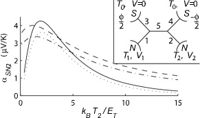
The observed behavior of the thermopower is not completely understood, but the major features can be explained. The first theoretical predictions were given by Claughton and Lambert (1996), who constructed a scattering theory to describe the effect of Andreev reflection on the thermoelectric properties of proximity systems. Based on their work, it was shown Heikkilä et al. (2000) that the presence of Andreev reflection can lead to a violation of the Mott relation. This means that a finite thermopower can arise even in the presence of electron-hole symmetry. Seviour and Volkov (2000b), Kogan et al. (2002), and Virtanen and Heikkilä (2004b, a) showed that in Andreev interferometers carrying a supercurrent, a large voltage can be induced by the temperature gradient both between the normal-metal reservoirs and between the normal metals and the superconducting contacts. Virtanen and Heikkilä (2004b) showed that in long junctions, the induced voltages between the two normal-metal reservoirs and the superconductors can be related to the temperature dependent equilibrium supercurrent flowing between the two superconductors via
| (47) |
Here , and are the resistances of the five wires defined in the inset of Fig. 7. This is in most situations the dominant term and it can be also phenomenologically argued based on the temperature dependence of the supercurrent and the conservation of total current (supercurrent plus quasiparticle current) in the circuit Virtanen and Heikkilä (2004b). A similar result can also be obtained in the quasiequilibrium limit for the linear-response thermopower Virtanen and Heikkilä (2004a). In addition to this term, the main correction in the long-junction limit comes from the anomalous coefficient ,
| (48) |
Here and is the length of wire . One finds that for a ”cross” system without the central wire (i.e., ), this term dominates . Further corrections to the result (47) are discussed by Kogan et al. (2002) and Virtanen and Heikkilä (2004a).
The above theoretical results explain the observed magnitude and temperature dependence of the thermopower and also predict an induced voltage oscillating with the phase . However, the thermopower calculated by Seviour and Volkov (2000b), Kogan et al. (2002) and Virtanen and Heikkilä (2004b, a) is always an antisymmetric function of , and it vanishes for a vanishing supercurrent in the junction (including all the correction terms). Therefore, the symmetric oscillations of cannot be explained with this theory.
The presence of the supercurrent breaks the time-reversal symmetry and hence the Onsager relation (see Eqs. (39) and below) need not to be valid for . Heikkilä, et al. predicted a nonequilibrium Peltier-type effect Heikkilä et al. (2003) where the supercurrent controls the local effective temperature in an out-of-equilibrium normal-metal wire. However, it seems that the induced changes are always smaller than those due to Joule heating and thus no real cooling can be realized with this setup.
II.7 Heat transport by phonons
When the electrons are thermalized by the phonons, they may also heat or cool the phonon system in the film. Therefore, it is important to know how these phonons further thermalize with the substrate, and ultimately with the heat bath on the sample holder that is typically cooled via external means (typically by either a dilution or a magnetic refrigerator). Albeit slow electron-phonon relaxation often poses the dominating thermal resistance in mesoscopic structures at low temperatures, the poor phonon thermal conduction itself can also prevent full thermal equilibration throughout the whole lattice. This is particularly the case when insulating geometric constrictions and thin films separate the electronic structure from the bulky phonon reservoir (see Fig. 1). In the present section we concentrate on the thermal transport in the part of the chain of Fig. 1 beyond the sub-systems determined by electronic properties of the structure.
The bulky three-dimensional bodies cease to conduct heat at low temperatures according to the well appreciated law in crystalline solids arising from Debye heat capacity via
| (49) |
where is the thermal conductivity and is the heat capacity per unit volume, is the speed of sound and is the mean free path of phonons in the solid Ashcroft and Mermin (1976). Thermal conductivity of glasses follows the universal law, as was discovered by Zeller and Pohl (1971), which dependence is approximately followed by non-crystalline materials in general Pobell (1996). These laws are to be contrasted to thermal conductivities of pure normal metals (Wiedemann-Franz law, c.f., below Eq. (39)). Despite the rapid weakening of thermal conductivity toward low temperatures, the dielectric materials in crystalline bulk are relatively good thermal conductors. One important observation here is that the absolute value of the bulk thermal conductivity in clean crystalline insulators at low temperatures does not provide the full basis of thermal analysis without a proper knowledge of the geometry of the structure, because the mean free paths often exceed the dimensions of the structures. For example, in pure silicon crystals, measured at sub-kelvin temperatures Klitsner and Pohl (1987), thermal conductivity Wm-1K, heat capacity JK-4m and velocity m/s imply by Eq. (49) a mean free path of mm, which is more than an order of magnitude longer than the thickness of a typical silicon wafer. Therefore phonons tend to propagate ballistically in silicon substrates.
What makes things even more interesting, but at the same time more complex, e.g., in terms of practical thermal design, is that at sub-kelvin temperatures the dominant thermal wavelength of the phonons, , is of the order of 0.1 m, and it can exceed 1 m at the low temperature end of a typical experiment (see discussion in Subs. II.3.2). A direct consequence of this fact is that the phonon systems in mesoscopic samples cannot typically be treated as three-dimensional, but the sub-wavelength dimensions determine the actual dimensionality of the phonon gas. Metallic thin films and narrow thin film wires, but also thin dielectric films and wires are to be treated with constraints due to the confinement of phonons in reduced dimensions.
The issue of how thermal conductivity and heat capacity of thin membranes and wires get modified due to geometrical constraints on the scale of the thermal wavelength of phonons has been addressed by several authors experimentally Leivo and Pekola (1998); Holmes et al. (1998); Woodcraft et al. (2000) and theoretically (see, e.g., Anghel et al. (1998); Kuhn et al. (2004)). The main conclusion is that structures with one or two dimensions restrict the propagation of (ballistic) phonons into the remaining ”large” dimensions, and thereby reduce the magnitude of the corresponding quantities and at typical sub-kelvin temperatures, but at the same time the temperature dependences get weaker.
In the limit of narrow short wires at low temperatures the phonon thermal conductance gets quantized, as was experimentally demonstrated by Schwab et al. (2000). This limit had been theoretically addressed by Angelescu et al. (1998), Rego and Kirczenow (1998) and Blencowe (1999), somewhat in analogy to the well-known Landauer result on electrical conduction through quasi-one-dimensional constrictions Landauer (1957). The quantum of thermal conductance is , and there are four phonon modes at low temperature due to four mechanical degrees of freedom each adding to the thermal conductance of the quantum wire. In an experiment, see Fig. 8 four such wires in parallel thus carried heat with conductance . There are remarkable differences, however, in this result as compared to the electrical quantized conductance. In the thermal case, only one quantized level of conductance, per wire, could be observed, and since the quantity transported is energy, the ”quantum” of thermal conductance carries in its expression besides the constants of nature.
The thermal boundary resistance (Kapitza resistance, after the Russian physicist P. Kapitza) between two bulk materials is due to acoustic mismatch Lounasmaa (1974). A remaining open issue is the question of thermal boundary resistance in a structure where at least one of the phonon baths facing each other is restricted, such that thermal phonons perpendicular to the interface do not exist in this particular subsystem. Classically the penetrating phonons need, however, to be perpendicular enough in order to avoid total reflection at the surface Pobell (1996). In practice though, the phonon systems in the two subsystems cannot be considered as independent. We are not aware of direct experimental investigations on this problem.
On the device level reduced dimensions can be beneficial, e.g., in isolating thermally those parts of the devices to be refrigerated from those of the surrounding heat bath. This has been the method by which NIS based phonon coolers, i.e., refrigerators of the lattice have been realized experimentally utilizing thin silicon nitride films and narrow silicon nitride bridges Manninen et al. (1997); Fisher et al. (1999); Luukanen et al. (2000); Clark et al. (2005). These devices are discussed in detail in Section V.C.
Detectors utilizing phonon engineering are discussed in Sec. IV.
II.8 Heat transport in a metallic reservoir
Energy dissipated per unit time in a biased mesoscopic structure is given quite generally as , where is the current through and is the voltage across the device. This power is often so large that its influence on the thermal budget has to be carefully considered when designing a circuit on a chip. For instance, the NIS cooler of Sec. V.3.1 has a coefficient of performance given by Eq. (79), with a typical value in the range 0.010.1. This simply means that the total power dissipated is 10 to 100 times higher than the net power one evacuates from the system of normal electrons. Yet this tiny fraction of the dissipated power is enough to cool the electron system far below the lattice temperature due to the weakness of electron–phonon coupling. This observation implies that 10 to 100 times higher dissipated power outside the normal island tends to overheat the connecting electrode significantly, again because of the weakness of the electron–phonon coupling. Therefore it is vitally important to make an effort to thermalize the connecting reservoirs to the surrounding thermal bath efficiently. In the case of normal-metal reservoirs, heat can be conveniently conducted along the electron gas to an electrode with a large volume in which electrons can then cool via electron–phonon relaxation. In the case of a superconducting reservoir, e.g., in a NIS refrigerator, the situation is more problematic because of the very weak thermal conductivity at temperatures well below the transition temperature . In this case the superconducting reservoirs should either be especially thick, or they should be attached to normal metal conductors (”quasiparticle traps”) as near as possible to the source of dissipation (see discussion in Sec. V.3.1). The latter approach is, however, not always welcome, because, especially in the case of a good metallic contact between the two conductors, the operation of the device itself can be harmfully affected by the superconducting proximity effect.
Let us consider heat transport in a normal metal reservoir. In the first example we approximate the reservoir geometry by a semi-circle, connected to a biased sample with a hot spot of radius at its origin (see the inset of Fig. 9 (b)). This hot spot can approximate, for example, a tunnel junction of area . The results depend only logarithmically on , and therefore its exact value is irrelevant when making estimates. We first assume that the electrons carry the heat away with negligible coupling to the lattice up to a distance . According to Eq. (23), we can then write the radial flux of heat in the quasiequilibrium limit in the form
| (50) |
where is the electronic thermal conductivity, is the conduction area at distance in a film of thickness , and is the temperature at radius . According to the Wiedemann-Franz law and the temperature independent residual electrical resistivity in metals, one has (see below Eq. (39)). With these assumptions, using Eq. (50), one finds a radial distribution of temperature
| (51) |
where and are two distances from the hot spot, and we defined the square resistance as . Thus making the reservoir thicker helps to thermalize it. The model above is strictly appropriate in the case where a thin film in form of a semi-circle is connected to a perfect thermal sink at its perimeter (at ). A more adequate model in a typical experimental case is obtained by assuming a uniform semi-infinite film connected at its side to a hot spot as above, but now assuming that the film thermalises via electron–phonon coupling. Using Eq. (50) and energy conservation one then obtains (see Sec. II.4)
| (52) |
where is the lattice temperature, and is the exponent of electron phonon relaxation, typically . We can write this equation into a dimensionless form
| (53) |
Here we have defined and , where is the length scale of temperature over which it relaxes towards .
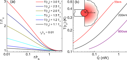
Figure 9 (a) shows the solutions of Eq. (53) for different values (1.1, 1.2, 1.5, 2.0, 2.5, and 3.0) of relative temperature rise . We see, indeed, that determines the relaxation length. To have a concrete example let us consider a copper film with thickness nm. For copper, using , we have WK-2m-1 and WK-5m-3, which leads to a healing length of 500 m at the bath temperature of 100 mK. The temperature rise versus input power has been plotted in Fig. 9 (b) for copper films with different thicknesses. In particular for nm, we obtain a linear response of /pW.
A superconducting reservoir, which is a necessity in some devices, poses a much more serious overheating problem. Heat is transported only by the unpaired electrons whose number is decreasing exponentially as towards low temperatures. Therefore the electronic thermal transport is reduced by approximately the same factor, as compared to the corresponding normal metal reservoir. Theoretically then is suppressed by nine orders of magnitude from the normal state value in aluminium at mK. It is obvious that in this case other thermal conduction channels, like electron–phonon relaxation, become relevant, but this is a serious problem in any case. At higher temperatures, say at , a significantly thicker superconducting reservoir can help Clark et al. (2004).
III Thermometry on mesoscopic scale
Any quantity that changes with temperature can in principle be used as a thermometer. Yet the usefulness of a particular thermometric quantity in each application is determined by how well it satisfies a number of other criteria. These include, with a weighting factor that depends on the particular application: wide operation range with simple and monotonic dependence on temperature, low self-heating, fast response and measurement time, ease of operation, immunity to external parameters, in particular to magnetic field, small size and small thermal mass. One further important issue in thermometry in general terms is the classification of thermometers into primary thermometers, i.e., those that provide the absolute temperature without calibration, and into secondary thermometers, which need a calibration at least at one known temperature. Primary thermometers are rare, they are typically difficult to operate, but nevertheless they are very valuable, e.g., in calibrating the secondary thermometers. The latter ones are often easier to operate and thereby more common in research laboratories and in industry.
In this review we discuss a few mesoscopic thermometers that can be used at cryogenic temperatures. Excellent and thorough reviews of general purpose cryogenic thermometers, other than mesoscopic ones, can be found in many text books and review articles, see, e.g., Lounasmaa (1974); Pobell (1996); Quinn (1983) and many references therein.
Modern micro- and nanolithography allows for new thermometer concepts and realizations where sensors can be very small, thermal relaxation times are typically short, but which generally do not allow except very tiny amounts of self-heating. The heat flux between electrons and phonons gets extremely weak at low temperatures whereby electrons decouple thermally from the lattice typically at sub-100 mK temperatures, unless special care is taken to avoid this. Therefore, especially at these low temperatures the lattice temperature and the electron temperature measured by such thermometers often deviate from each other. An important example of this is the electron temperature in NIS electron coolers to be discussed in Section V.
A typical electron thermometer relies on a fairly easily and accurately measurable quantity that is related to the electron energy distribution function via
| (54) |
Here the kernel describes the process which is used to measure and is a functional of . The quantity typically refers to an average current or voltage, in which case is a linear function of with some constant function ; or it can refer to the noise power, in which case is quadratic in . For the thermometer to be easy to calibrate, should be a simple function dependent only on a few parameters that need to be calibrated. Moreover, if has sufficiently sharp features, it can be used to measure the shape of also in the nonequilibrium limit.
III.1 Hybrid junctions
Tunnelling characteristics through a barrier separating two conductors with non-equal densities of states (DOSs) are usually temperature dependent. The barrier B may be a solid insulating layer (I), a Schottky barrier formed between a semiconductor and a metal (Sc), a vacuum gap (I), or a normal metal weak link (N). We are going to discuss thermometers based on tunnelling in a CBC’ structure. C and C’ stand for a normal metal (N), a superconductor (S), or a semiconductor (Sm). As it turns out, the current-voltage () characteristics of the simplest combination, i.e., of a NIN tunnel junction, exhibit no temperature dependence in the limit of a very high tunnel barrier. Yet NIN junctions form elements of presently actively investigated thermometers (Coulomb blockade thermometer and shot noise thermometer) to be discussed separately. The NIN junction based thermometers are suitable for general purpose thermometry, because their characteristics are typically not sensitive to external magnetic fields. Superconductor based junctions are, on the contrary, normally extremely sensitive to magnetic fields, and therefore they are suitable only in experiments where external fields can be avoided or at least accurately controlled.
In SBS’ junctions one has to distinguish between two tunnelling mechanisms, Cooper pair tunnelling (Josephson effect) and quasiparticle tunnelling. The former occurs at low bias voltage and temperature, whereas the latter is enhanced by increased temperature and bias voltage. In the beginning of this section we discuss quasiparticle tunnelling only.
Let us consider tunnelling between two normal-metal conductors through an insulating barrier. I-V characteristics of such a junction were given by Eq. (29). We assume quasi-equilibrium with temperatures , on the two sides of the barrier. Since to high precision at all relevant energies ( Fermi energy), Eq. (29) can be integrated easily to yield . Therefore the characteristics are ohmic, and they do not depend on temperature, and a NIN junction appears to be unsuitable for thermometry. There is, however, a weak correction to this result, due to the finite height of the tunnel barrier Simmons (1963a), which will be discussed in subsection III.D.
III.1.1 NIS thermometer
As a first example of an on-chip thermometer, let us discuss a tunnel junction between a normal metal and a superconductor (NIS junction) Rowell and Tsui (1976). I-V characteristics of a NIS junction have the very important property that they depend on the temperature of the N electrode only, which is easily verified, e.g., by writing of Eq. (29) with and in a symmetric form
| (55) |
This insensitivity to the temperature of the superconductor holds naturally only up to temperatures where the superconducting energy gap can be assumed to have its zero-temperature value. This is true in practice up to .
Employing Eq. (55) one finds that a measurement of voltage at a constant current yields a direct measure of , and in quasi-equilibrium, where the distribution follows thermal Fermi-Dirac distribution, it also yields temperature in principle without fit parameters. Figure 10 (a) shows the calculated I-V characteristics of a NIS junction at a few temperatures . Figure 10 (b) gives the corresponding thermometer calibration: junction voltage has been plotted against temperature at a few values of (constant) measuring current.
A NIS thermometer has a number of features which make it attractive in applications. The sensing element can be made very small and thereby NIS junctions can probe temperature locally and detect temperature gradients. Junctions made by electron beam lithography can be much smaller than 1 m in linear dimension Nahum and Martinis (1993). Using a scanning tunnelling microscope with a superconducting tip as a NIS junction one can most likely probe the temperature of the surface locally on nanometer scales in an instrument like those of Moussy et al. (2001); Vinet et al. (2001). Self-heating can be made very small by operating in the sub-gap voltage range (see Fig. 10), where current is very small. The superconducting probe is thermally decoupled from the normal region whose temperature is monitored by it. The drawbacks of this technique include high sensitivity to external magnetic field, high impedance of the sensor especially at low temperatures, and sample-to-sample deviations from the ideal theoretical behaviour. Due to this last reason, a NIS junction can hardly be considered as a primary thermometer: deviations arise especially at low temperatures, one prominent problem is saturation due to subgap leakage due to non-zero DOS within the gap and Andreev reflection.
A fast version of a NIS thermometer was implemented by Schmidt et al. (2003). They achieved sub-s readout times (bandwidth about 100 MHz) by imbedding the NIS junction in an resonant circuit. This rf-NIS read-out is possibly very helpful in studying thermal relaxation rates in metals, and in fast far-infrared bolometry.
NIS junction thermometry has been applied in x-ray detectors Nahum et al. (1993), far-infrared bolometers Mees et al. (1991); Chouvaev et al. (1999), in probing the energy distribution of electrons in a metal Pothier et al. (1997a), and as a thermometer in electronic coolers at sub-kelvin temperatures Nahum et al. (1994); Leivo et al. (1996). It has also been suggested to be used as a far-infrared photon counter Anghel and Kuzmin (2003). In many of the application fields of a NIS thermometer it is not the only choice: for example, a superconducting transition edge sensor (TES) can be used very conveniently in the bolometry and calorimetry applications (see Sec. IV).
III.1.2 SIS thermometer
A tunnel junction between two superconductors supports supercurrent, whose critical value has a magnitude which depends on temperature according to Ambegaokar and Baratoff (1963): . This can naturally be used to indicate temperature because of the temperature dependence of the energy gap and the explicit hyperbolic dependence on . Yet, these dependencies are exponentially weak at low temperatures. Another possibility is to suppress by magnetic field, e.g., in a SQUID configuration, and to work at non-zero bias voltage and measure the quasiparticle current, which can be estimated by Eq. (29) again with both DOSs given by Eq. (12) now. The resulting current depends approximately exponentially on temperature, but the favourable fact is that the absolute magnitude of the current is increased because it is proportional to the product of the two almost infinite DOSs matching at low bias voltages, and, in practical terms, the method as a probe of a quasiparticle distribution is more robust against magnetic noise. Figure 11 shows the calculated and measured dependences of at a few values of temperature . Although the curves corresponding to the lowest temperatures almost overlap here, it is straightforward to verify that a standard measurement of current can resolve temperatures down to below using an ordinary tunnel junction.
SIS junctions have not found much use as thermometers in the traditional sense, but they are extensively investigated and used as photon and particle detectors because of their high energy resolution (see, e.g., Booth and Goldie (1996) and Section IV). In this context SIS detectors are called STJ detectors, i.e., superconducting tunnel junction detectors. Another application of SIS structures is their use as mixers Tinkham (1996). While superficially similar to STJ detectors, their theory and operation differ significantly from each other. SIS junctions are also suitable for studies of quasiparticle dynamics and fluctuations in general (see, e.g., Wilson et al. (2001)).
III.1.3 Proximity effect thermometry
For applications requiring low-impedance ( ) thermometers at sub-micron scale, the use of clean NS contacts may be more preferable than thermometers applying tunnel contacts. In an SNS system, one may again employ either the supercurrent or quasiparticle current as the thermometer. For a given phase between the two superconductors, the former can be expressed through Belzig et al. (1999)
| (56) |
where is the normal-state resistance of the weak link, is the spectral supercurrent Heikkilä et al. (2002), and the energies are measured from the chemical potential of the superconductors. Hence, the supercurrent has the form of Eq. (54). In practice, one does not necessarily measure , but the critical current . In diffusive junctions, this is obtained typically for near , although the maximum point depends slightly on temperature.
The problem in SNS thermometry is in the fact that the supercurrent spectrum depends on the quality of the interface, on the specific geometry of the system, and most importantly, on the distance between the two superconductors compared to the superconducting coherence length Heikkilä et al. (2002). Therefore, dependence is not universal. However, the size of the junction can be tuned to meet the specific temperature range of interest. In the limit of short junctions, Kulik and Omel’yanchuk (1978), the temperature scale for the critical current is given by the superconducting energy gap and for , the supercurrent depends very weakly on the temperature. In a typical case nm, and thus already a weak link with of the order of 1 m, easily realisable by standard lithography techniques, lies in the ”long” limit. There, the critical current is Zaikin and Zharkov (1981). This equation is valid for . Here and the prefactor depends on the geometry Heikkilä et al. (2002), for example for a two-probe configuration . The exponential temperature dependence and the crossover between the long- and short-junction limits were experimentally investigated by Dubos et al. (2001) and the above theoretical predictions were confirmed.
Using a four-probe configuration with SNS junctions of different lengths, Jiang et al. (2003) exploited the strong temperature dependence of the supercurrent to measure the local temperature. The device worked in the regime where part of the junctions were in the supercurrent-carrying state and part of them in the dissipative state. In the limit where supercurrent is completely suppressed, there is still a weaker temperature dependence of the conductance, due to the proximity-effect correction (c.f., Eq. (46)) Charlat et al. (1996). This can also be used for thermometry Aumentado et al. (1999), but due to the much smaller effect of temperature on the conductance, it is less sensitive.
III.2 Coulomb blockade thermometer, CBT
Single electron tunnelling (SET) effects were foreseen in micro-lithographic structures in the middle of 1980’s Averin and Likharev (1986). Such effects in granular structures had been known to exist already much earlier Neugebauer and Webb (1962); Giaever and Zeller (1968); Lambe and Jaklevic (1969). The first lithographic SET device was demonstrated by Fulton and Dolan (1987). Since that time SET effects have formed a strong subfield in mesoscopic physics. Typically SET devices operate in the full Coulomb blockade regime, where temperature is so low that its influence on electrical transport characteristics can be neglected; at low bias voltages current is blocked due to the charging energy of single electrons. Coulomb blockade thermometer (CBT) operates in a different regime, where single electron effects still play a role but temperature predominantly influences the electrical transport characteristics Pekola et al. (1994); Farhangfar et al. (1997); Bergsten et al. (2001); Meschke et al. (2004). CBT is a primary thermometer, whose operation is based on competition between thermal energy at temperature , electrostatic energy at bias voltage , and charging energy due to extra or missing individual electrons with unit of charging energy , where is the effective capacitance of the system. Figure 12 shows an SEM micrograph of a part of a typical CBT sensor suitable for the temperature range 0.021 K. This sensor consists of four parallel one-dimensional arrays with 40 junctions in each.
In the partial Coulomb blockade regime the characteristics of a CBT array with junctions in series do not display a sharp Coulomb blockade gap, but, instead, they are smeared over a bias range . The asymptotes of the at large positive and negative voltages have, however, the same offsets as at low , determined by the Coulomb gap. In the partial Coulomb blockade regime it is convenient to measure not the directly, but the differential conductance, i.e., the slope of the curve, , vs. . The result is a nearly bell shaped dip in conductance around zero bias. Figure 13 illustrates a measured conductance curve, scaled by asymptotic conductance at large positive and negative voltages. The important property of this characteristic is that the full width of this dip at half minimum, , approximately proportional to , determines the temperature without any fit, or any material or geometry dependent parameters, i.e., it is a primary measure of temperature. In the lowest order in , one finds for the symmetric linear array of junctions of capacitance in series Pekola et al. (1994); Farhangfar et al. (1997)
| (57) |
For such an array and . The full width at half minimum of the conductance dip has the value
| (58) |
which allows one to determine without calibration.
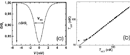
It is often convenient to make use of the secondary mode of CBT, in which one measures the depth of the dip, , which is proportional to the inverse temperature, again in the lowest order in :
| (59) |
Measuring the inflection point of the conductance curve provides an alternative means to determine without calibration. In Bergsten et al. (2001) this technique was used for fast thermometry on two dimensional junction arrays. A simple and fast alternative measurement of CBT can be achieved by detecting the third harmonic current in a pure AC voltage biased configuration Meschke et al. (2005).
There are corrections to results (57), (58) and (59) due to both next order terms in and due to non-uniformities in the array Farhangfar et al. (1997). Higher order corrections do sustain the primary nature of CBT, which implies wider temperature range of operation. The primary nature of the conductance curve exhibited by Eq. (57) through the bias dependence is preserved also irrespective of the capacitances of the array, even if they would not be equal. Only a non-uniform distribution of tunnel resistances leads to a deviation from the basic result of bias dependence of Eq. (57). Fortunately the influence of the inhomogeneity on temperature reading is quite weak, and it leads typically to less than 1 % systematic error in .
The useful temperature range of a CBT array is limited at high temperature by the vanishing signal (). In practice the dip must be deeper than % to be resolvable from the background. The low temperature end of the useful temperature range is set by the appearance of charge sensitivity of the device, i.e., the background charges start to influence the characteristics of the thermometer. This happens when Farhangfar et al. (1997). With these conditions it is obvious that the dynamic range of one CBT sensor spans about two decades in temperature.
The absolute temperature range of CBT techniques is presently mainly limited by materials issues. At high temperatures, the measuring bias range gets wider, , and the conductance becomes bias dependent also due to the finite (energy) height of the tunnel barrier Simmons (1963a); Gloos et al. (2000). Because of this, the present high temperature limit of CBTs is several tens of K. The (absolute) low temperature end of the CBT technique is determined by self-heating due to biasing the device. One can measure temperatures reliably down to about 20 mK at present with better than 1 % absolute accuracy in the range 0.054 K, and about 3 % down to 20 mK Meschke et al. (2004).
Immunity to magnetic field is a desired but rare property among thermometers. For instance, resistance thermometers have usually strong magnetoresistance. Therefore one could expect CBT to be also ”magnetoresistive”. On the contrary, CBT has proven to be immune to even the strongest magnetic fields ( T) Pekola et al. (1998, 2002); van der Linden and Behnia (2004). This happens because CBT operation is based on electrostatic properties: tunnelling rates are determined by charging energies. Hence, CBT should be perfectly immune to magnetic field as long as energies of electrons with up and down spins do not split appreciably, which is always the case in experiments.
Coulomb blockade is also a suitable probe of non-equilibrium energy distributions as demonstrated by Anthore et al. (2003).
III.3 Shot noise thermometer, SNT
Noise current or voltage of a resistor (resistance ) has been known to yield absolute temperature since 1920’s Johnson (1928); Nyquist (1928); Blanter and Büttiker (2000). Till very recently only equilibrium noise, i.e., noise across an unbiased resistor, was employed to measure temperature. In this case Johnson noise voltage and current squared have expectation values , where is the frequency band of the measurement. In other words, the current spectral density is given by , and voltage spectral density by . There are several critical issues in measuring temperature through Johnson noise. First, the bandwidth has to be known exactly. Secondly, the small signal has to be amplified, and the gain must be known to high accuracy. Thirdly, the noise signal becomes extremely small at cryogenic temperatures, which in turn means that the measurement has to be able to detect a very small current or voltage, and at the same time no other noise sources should cause comparable voltages or currents.
Success in noise thermometry depends critically on the performance of the amplifiers used to detect the tiny noise current (or voltage). Constant progress in improving SQUIDs (Superconducting Quantum Interference Device) and in optimizing their operation has pushed the lowest temperature measurable by a Johnson noise thermometer down to below 1 mK Lusher et al. (2001).
It is not only the equilibrium noise that can be useful in thermometry. In the opposite limit, at , the dominating noise, e.g., in tunnel junctions, is shot noise Schottky (1918); Blanter and Büttiker (2000), whose current spectral density is given asymptotically by . Fano factor equals for a tunnel junction. The way Johnson noise transforms into shot noise upon increasing the bias obeys the relation (see Eq. (34a) with , and, e.g., van der Ziel (1986))
| (60) |
At , Eq. (60) obtains the Poisson expression above, whereas at it assumes the thermal Johnson form .
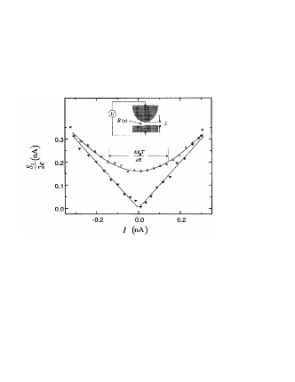
Temperature dependent cross-over characteristics from Johnson to shot noise according to Eq. (60) have been demonstrated experimentally, e.g., in scanning tunnelling microscope experiments Birk et al. (1995) as shown in Fig. 14. Recently, Spietz et al. (2003) employed this cross-over in a lithographic tunnel junction between metallic films for thermometry (shot noise thermometer, SNT) in the temperature range from few tens of mK up to room temperature. At both ends of this range there are systematic errors in the reading, which can possibly be corrected by a more careful design of the sensor. In a rather wide range around 1 K (about 0.110 K), the absolute accuracy is better than 1 %. The crossover voltage depends only on , which means that the thermometer is indeed primary; ideally the temperature reading does not depend on the materials or geometry of the sensor. Figure 15 shows the experimental data of Spietz et al. (2003) at several temperatures: normalised (by Johnson noise) current noise has been plotted against normalised voltage , whereby all curves at different temperatures should lie at . As seen in the bottom half of the figure, the residuals are smallest around 1 K.
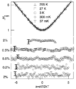
As discussed above, noise measurements are difficult to perform especially at low temperature where signal gets very small. At any temperature it is critically important to know the frequency window of the measurement and the gains in the amplifiers in Johnson noise thermometry. Yet the SNT avoids some of these problems. It is based on the cross-over between two noise mechanisms, both of which represent white noise, whereby the frequency window is ideally not a concern, since the same readout system is used in all the bias regimes. Moreover, the gains of the amplifiers are not that critical either because of the same argument. One can also use relatively high bandwidth which increases the absolute noise signal to be measured, and thereby makes the measurement faster.
The SNT technique has a few further attractive features. It is likely that its operation can be easily extended up to higher temperatures despite the deviations observed in the first experiments. The sensor consists of just one, relatively large size tunnel junction, which means that it is easy to fabricate with high precision. Also it is likely, although not yet demonstrated, that the SNT is not sensitive to magnetic field, since its operation is based on tunnelling characteristics in a NIN tunnel junction as in CBT.
Finally, noise measurements can in principle be used to measure the distribution function in non-equilibrium as well, as proposed by Pistolesi et al. (2004).
III.4 Thermometry based on the temperature dependent conductance of planar tunnel junctions
The effect of temperature on the current across a tunnel barrier with finite height is a suitable basis for thermometry in a wide temperature range Gloos et al. (2000). Simmons (1963a) showed that the tunnelling conductance at zero bias across a thin insulating barrier depends on temperature as
| (61) |
where is the temperature independent part of conductance and the scaling temperature depends on the barrier height . For a rectangular barrier of width one has , where is the effective mass of the electrons within the insulating barrier. Experiments over a temperature range from 50 K up to 400 K on Al-AlOx-Al tunnel junctions have demonstrated that Eq. (61) is obeyed remarkably well Gloos et al. (2000); Suoknuuti et al. (2001). Moreover, in these measurements the scaling temperature was found to be K in all samples, without a clear dependence on the specific (zero temperature) conductance of the barrier, which varied over three orders of magnitude from S/m2 up to 3000 S/m2. This property makes the method attractive in wide range thermometry, and can indeed be considered as a material specific, but geometry and thickness independent parameter up to a certain accuracy.
III.5 Anderson-insulator thin film thermometry
As regards to temperature read-out of micro-calorimetric devices, resistive thin film thermometers near the metal-insulator transition (MIT) are relatively popular. Electrical resistivity properties on both sides of the MIT are rather well understood Belitz and Kirkpatrick (1994), and in general resistance of such thin films shows strong temperature dependence, suitable for thermometry and in particular for calorimetry. On the insulator side resistivity is determined by hopping, and it has typically temperature dependence, with and constants. On the metallic side, weaker dependence can be found. In practice, both NbxSi1-x Denlinger et al. (1994); Marnieros et al. (1999, 2000) and NbN Fominaya et al. (1997); Bourgeois et al. (2005) thin film based thermometers have been successfully employed. The suitable conduction regime can be tailored by adjusting () in electron beam co-evaporation Denlinger et al. (1994) or in dc magnetron sputtering of Nb in a nitrogen atmosphere Fominaya et al. (1997).
Bolometric and calorimetric radiation detectors are discussed in detail in Sec. IV. Here we briefly mention the application of a NbN thermometer in a measurement of the heat capacity of 450 000 superconducting thin film loops on a silicon membrane Bourgeois et al. (2005), see Fig. 16. The heat capacity of the loops is proportional to their total mass, which was about 80 ng in this case. Vortices entering simultaneously into the 450 000 loops under application of magnetic field could be observed. A similar measurement Lindell et al. (2000), employing a NIS thermometer could resolve the specific heat jump at of 14 thin film titanium disks with total mass of 1 ng on a silicon nitride membrane.
IV Thermal detectors and their characteristics
The absorption of electromagnetic radiation by matter almost always ends in the situation where the incident optical power has, possibly via cascades of different physical processes, transformed into aggravated random motion of lattice ions, i.e. into heat. Here lies the fundamental principle behind the thermal detection of radiation: the transformation of the input electromagnetic energy to heat. In many cases, this state of maximum entropy has lost all the coherent properties that the incident radiation might have possessed, but yet there is information in this messy final state of the system: the rise in the system temperature. In this section, we give a short overview of thermal detectors, their theory and operation, and discuss some examples of thermal detectors and their applications.
There is a very small difference between thermometry and bolometry, the thermal radiation detection. Yet thermometry often implies measurement of temperature changes over a large fractional temperature range, whereas in the typical bolometric application, the observed temperature variations are extremely small. This allows us in the following to concentrate on the limit of small temperature changes around some mean well-defined value, i.e., we assume the operation in the quasiequilibrium regime (see Sec. II). In essence, bolometry is really high-precision thermometry, nothing more, with the added ingredient of finding efficient ways of coupling incident radiation to the device.
Although thermal detectors have developed enormous diversity since their introduction in 1880 by Samuel P. Langley, and major advances in the way the temperature rise is measured and the detectors are constructed have been made, the basic principle remains the same. The operating principle of a thermal detector can be traced back to the generalized thermal model, shown in Fig. 1. The four main parts of a thermal detector are a thermally isolated element, a thermal link with a thermal conductance (here or ), a thermal sensing element (i.e., a thermometer), and a coupling structure (e.g., an impedance matching structure for electromagnetic radiation) that serves to maximize the absorbtion of the incident radiation, be it in the forms of alpha particles or microwaves.
IV.1 Effect of operating temperature on the performance of thermal detectors
Regardless of the exact architecture of the thermal detector, lowering the operating temperature will improve the performance significantly. This fact introduces the cooling techniques to the use of thermal detectors. Because of the diversity of the technological approaches it is hard to summarize the effect of the operating temperature in a fully universal fashion. However, some general trends can be evaluated. The figure of merit for thermal detectors is the noise equivalent power (NEP), which relates to the signal to noise ratio by , where is the incident optical power and is the post-detection integration time. The limiting NEP for an optimized thermal detector is given by the thermal fluctuation noise (TFN) arising from random fluctuations of energy across the thermal link with a thermal conductance which result in variations in the temperature of the device (see also discussion in Subs. II.5.2). The TFN limited noise equivalent power (NEP) in the linear order is given by the fluctuation-dissipation result Mather (1982)
| (64) |
with the two cases relating the temperature dependence to the location of the thermal bottleneck. The expression for the lattice isolated case is generally valid at temperatures with the Debye temperature of the insulating material. The temperature is the highest of the temperatures present in the system, i.e., the temperature of the thermally isolated element or that of the heat sink.
Refrigeration, combined with the advances in nanolithography techniques have recently opened a whole new realm for the application of electron-phonon decoupling to improve the thermal isolation of bolometric detectors. The operation of these so-called hot electron devices is usually limited to low ( 1 K) temperatures and very small thermally active volumes as the TFN between the electron gas and the lattice is given by Golwala et al. (1997) where varies between 1-4 nWmK5 in metals (See Table 1). The use of the lattice for the thermal isolation lends itself to operation over much broader temperature range as the geometry of the thermal link can be used to increase the thermal resistance.
Typically, the bath temperatures of cryogenic thermal detectors are centered around four temperature ranges: 4.2 K, the boiling temperature of liquid He at 1 atm, around 300 mK a temperature attainable with 3He sorption refrigerators, around 100 mK, easily attainable using a compact adiabatic demagnetization refrigerator (ADR), or below 50 mK, when a dilution refrigerator is used. In the recent years, the use of electronic refrigeration has become appealing with the development of the SINIS coolers. These coolers could enable the operation of thermal detectors at a much lower temperature than is ’apparent’ to the user. For instance, the 3He sorption coolers are quite attracting due to their compactness, low cost and simple operation. Used together with a SINIS cooler would allow for an affordable cryogenic detector system without having to sacrifice in performance.
Since the thermal fluctuation noise in a thermal detector is proportional to , maximum performance improvement is achieved by the reduction of the bath temperature Anghel et al. (2001). Modest performance increase is possible with direct electronic cooling, such as is the case in many of the SINIS bolometer experiments.
In addition to improved noise performance, direct coupling of a SINIS cooler to a thermal detector could allow for increasing the dynamic range of for example bolometers based on transition edge sensors (TES): A SINIS cooler can be used to draw a constant power from a TES that would otherwise saturate due to an optical load.
IV.2 Bolometers: Continuous excitation
Thermal detectors that are used to detect variations in the incident flux of photons or particles are called bolometers (from the Greek word bol - beam). This condition is generally met when the mean time between incident quanta of energy that arrive at the detector is much shorter than the recovery time of the bolometer 333The opposite (calorimetric) limit will be discussed in section IV.3. The bolometric operating principle is very simple: Change in the incident optical power creates a change in the temperature of a thermally isolated element by . A sensitive thermometer is used to measure this temperature change. The recovery time is determined by the heat capacity of the bolometer, and the thermal conductance with , analogously to an electrical circuit.
Bolometric detectors remain popular today, 125 years after their first introduction. Probably the most important advantage of thermal detectors is their versatility: Bolometers can detect radiation from -particles to radio waves, their dynamic range can be easily adapted for a variety of signal or background levels. As an extreme example, bolometers have been used to detect infrared radiation from nuclear fireballs Stubbs and Phillips (1960), and the cosmic microwave background. Lamarre et al. (2003).
In the early days, bolometers typically utilized hand-crafted construction (dental floss, cigarette paper and balsa wood are examples of typical materials used in the construction) Davis et al. (1964). If detecting electromagnetic waves, typically the absorber consisted of a metal with a suitable thickness yielding a square resistance of 377 , i.e. matching the impedance of the vacuum. Further improvements on matching were achieved by placing the bolometer in a resonant cavity. One major setback with bolometers in their early days was unavoidably slow speed, caused by the large heat capacity resulting from the macroscopic size of the components used. The dawn of modern microfabrication techniques has all but eliminated this shortcoming, with bolometers of high sensitivity achieving time constants as short as a few hundred nanoseconds.
Today, the most common type of cryogenic resistive bolometers utilize transition edge sensors for the thermometry. In a TES bolometer, a superconducting film with a critical temperature is biased within its superconductor - normal metal transition where small changes in the film temperature result to changes in the current through the device (or the voltage across the film). In most cases, the TES consists of two or more sandwiched superconductor-normal metal layers. The relative thicknesses of the S and N layers are used to tune the transition temperature to a desirable value by the proximity effect.
Transition-edge sensors are by no means a novel type of a thermal detector, as first suggestions for their use came out already in the late thirties Andrews (1938); Goetz (1939), and first experimental results by 1941 Andrews (1941). Two principal problems prohibited the wide use of this type of thermal detectors for some fifty years: Typically the normal-state resistance of the superconducting films was too low in order to obtain adequate noise matching with field effect transistor (FET) preamplifiers, and the lack of good transimpedance amplifiers usually required the films to be current biased with a voltage readout. This introduced a requirement to tune the heat bath temperature very accurately within the narrow range of temperatures in the superconducting transition. This also made the devices exceedingly sensitive to small variations in the bath temperature, introducing stringent requirements for the heat bath stability.
These limitations can be overcome by the use of an external negative feedback circuit that maintains the film within its transition temperature and above the bath temperature. Such an approach was adopted by Clarke et al. (1977), who were able to demonstrate NEP= W at an operating temperature of 1.27 K, using a transformer-coupled FET as the voltage readout. Introducing a negative feedback has similar advantages as in the case of operational amplifiers: linearity is improved, sensitivity to internal parameters of the amplifier (or bolometer) is reduced, and the speed is increased. Interestingly, the use of an external negative feedback in conjunction with superconducting transition edge sensors never found widespread use, possibly due to the (slightly) more complicated read-out architecture, and the need for a matching transformer.
The breakthrough of TESs came in 1995, when superconducting quantum interference device (SQUID) ammeters, which are inherently well suited in matching to low load impedances, were introduced as the readout devices for TESs Irwin et al. (1995a); Irwin (1995). This allowed for the use of voltage biasing, which introduces strong negative electrothermal feedback (ETF) that causes the thermally isolated film to self-regulate within its superconducting transition. The local nature of the ETF makes the operation of these detectors very simple as no external regulation is necessary. As with an external negative feedback, an important advantage of the voltage biased TES is the fact that once the bath temperature is below , the need for bath temperature regulation is significantly relaxed. Finally, the increased speed due to the strong negative ETF increases the bandwidth of the detector, allowing for either detecting faster signal changes in a bolometer, or higher count rates in a calorimeter. A comprehensive review of the theory and operation of voltage biased TESs has been recently published Irwin and Hilton (2005).
The behaviour of thermal detectors is generally well understood. In the following discussion we shall summarize the main results for the theory of thermal detectors. The results are quite generally applicable to any resistive bolometers, but the treatment is geared towards voltage biased TES, firstly as they are currently the most popular type of thermal detectors, and secondly because the electrothermal effects are very prominent in these devices, having a major impact on the device speed and linearity.
We start by writing the equation governing the thermal circuit (here we limit the discussion to a simple case of one thermal resistance and heat capacity). Generally, the power flow to the heat sink is given by , where is a constant which depends on materials parameters and the geometry of the link. The time dependence of the bolometer temperature can be solved from the heat equation for a bolometer with a bias point resistance of absorbing a time-varying optical signal (c.f., Eq. (23)):
| (65) |
where is used to denote the temperature change due to the signal power and describes the incoming heat flow due to the detector bias. Equating the steady state components of the equation yields , from which one can obtain the result for the average operating temperature of the bolometer, given by where an average thermal conductance is defined by .
The electrothermal feedback manifests itself through the fact that the change in input signal power modifies the bias dissipation, an effect described by the last term in Eq. (65). Taking a closer look at the temperature change we obtain
| (66) |
where is the dynamic thermal conductance. Now, considering the electrothermal term
| (67) |
where describes the sensitivity of the detector resistance to the temperature changes and is the effect of the bias circuit (with an embedding impedance of ) on the ETF. Taking into account the thermal cut-off of the bolometer, the frequency-dependent loop gain is defined as
| (68) |
where and is the intrinsic thermal time constant of the bolometer. The electro-thermal loop gain describes the effect of varying incident optical power to the bias power dissipated in the detector. For positive bolometers with the loop gain is positive for current bias (since Re) and negative for voltage bias (as Re). For bolometers with a negative temperature coefficient of resistance the situation is reversed. For metallic bolometers operated at room temperature and the loop gain is typically small (1) so that the role of ETF is negligible. On the contrary, superconducting detectors with and some three orders of magnitude smaller than for room temperature devices can have large loop gain (), so that ETF plays a significant role in the detector characteristics. A major impact of negative ETF is that the bolometer time constant is reduced from to . This reduction in the time constant is one of the major benefits of strong negative ETF.
Voltage biasing conditions are typically reached by driving a constant current through a parallel combination of the bolometer and a load resistor . As long as , the bolometer is effectively voltage biased. The responsivity of a voltage biased bolometer can be derived as follows: The current responsivity is defined as . Using Eqs. (66), (67) and (68), , and , the result for the current responsivity becomes
| (69) |
In the limiting case at with (perfect voltage bias) and ,
| (70) |
In order to evaluate the NEP for a bolometer, a discussion on the noise sources in bolometers is merited. In general, the NEP, noise spectral density , and responsivity are related by NEP, where the subscripts refer to voltage or current noise and responsivity, respectively. The noise in bolometers is due to several uncorrelated sources. The most important of them is the thermal fluctuation noise, mentioned already above. Generally, this contribution is given by
| (71) |
Here describes the effect of the temperature gradient across the thermal link between the sensor and the heat sink Mather (1982) in the diffusive limit (i.e., no ballistic heat transport present) as
| (72) |
Here we assumed that the thermal conductivities obey . For resistive bolometers, another important contribution to the NEP is due to the Johnson noise, given by
| (73) |
In addition to these noise sources, the current noise of the amplifier, , adds a contribution . The total NEP of a bolometer is then
| (74) |
where the slightly ambiguous contribution encompasses various contributions from additional external and internal noise sources. Typical excess external noise contributions arise from heat bath temperature fluctuations and pickup in the cabling to name a few. In addition to the external excessive noise, it has in recent years become clear that there are also internal noise sources that are not fully accounted for. For instance, TESs with significant internal thermal resistance can no longer be treated using the simple lumped element model, and they suffer from internal thermal fluctuation noise (ITFN), adding a contribution Hoevers et al. (2000)
| (75) |
where is the Lorenz number.
For some devices, these noise sources are sufficient to explain all the observed noise. However, many groups are developing X-ray microcalorimeters (see below) which are often operated at a small fraction of the normal state resistance exhibit noise that increases rapidly as the bias point resistance is decreased, and has a significant influence on the performance of the detectors. Several possible explanations have been put forth, e.g., noise arising from the fluctuations in magnetic domains or phase-slip lines Knoedler (1983); Wollman et al. (1997). A systematic study of the excess noise in different TES geometries has been published recently Ullom et al. (2004), showing that there exists a clear correlation between and the observed excess noise, with the magnitude of the excess noise scaling roughly as . A quantitative agreement with the measured excess noise spectrum has so far been achieved in one experiment Luukanen et al. (2003), where the TES consisted of an annular (so called Corbino) geometry with a superconducting center contact, and a concentric current return at the outer perimeter of the annular TES. This geometry results in strictly radial current flow, enabling a simple analytical expression for the current density in the TES. The dependence in the current density together with a small radial temperature gradient causes the TES to separate to two annular superconducting and normal state regions.
For any system undergoing a second order phase transition, order parameter fluctuations will take place. The excess noise arises from the thermally driven fluctuation of the phase boundary which manifest as resistance fluctuations. The volume associated with the order parameter fluctuation can be obtained by noting that the Ginzburg-Landau free energy associated with the fluctuation is . As the TES is biased towards smaller , the relative contribution of the order parameter fluctuations becomes larger until it fully dominates over the other noise contributions. For the Corbino-geometry TES, the contribution due to the fluctuation superconductivity noise (FSN) to the NEP is
| (76) |
where K is a constant dependent on the TES parameters.
So far, this noise model has not successfully been applied to TESs in the more conventional square geometry, mainly due to the fact that the current distribution varies with bias point and is not easily calculable. A solution could be obtained by solving the full 2D Ginzburg-Landau equations for a square geometry.
IV.2.1 Hot electron bolometers
In principle, modern bolometers can be artificially divided into two major sub-classes depending on where the dominant thermal bottleneck lies. The so-called hot-electron bolometers (HEBs) utilize the decoupling of the electron gas in a metal or a semiconductor from the phonon heat bath. The earliest HEBs were based on InSb, where the weak coupling of the electrons to the lattice at temperatures around 4 K allows the electrons to be heated to a temperature significantly above that of the lattice even in a bulk sample. Mobility in InSb is limited by ionized impurity scattering which results in decreasing resistivity with an increasing electric field. This is the basis of the detection mechanism Rollin (1961); Brown (1984). Often HEBs have sufficient speed for mixing, and in fact HEB mixers are a current topic of considerable interest. Most HEBs mixers operate at 4 K, and in order to maintain our focus on phenomena and devices at temperatures below 1 K, we unfortunately will not discuss them within this review.
HEB direct detectors Richards (1994); Ali et al. (2003); Karasik et al. (2003) have been a subject of considerable interest, but in general a full optical demonstration remains to be carried out. The attractive features of such devices include very short time constant (well below 1 s), potentially very good NEP performance (below W/ when operated at or below 0.3 K), and simple construction that does not require surface micromachining steps. The architecture is essentially very similar to that of the HEB mixers: a small superconducting TES film coupled to the feed of a lithographic antenna. The application of the SQUID readout scheme utilized in typical hot phonon microbolometers and microcalorimeters might not be as straightforward as one could expect as the introduction of the SQUID input coil inductance to the voltage biasing circuit can make the system unstable due to the interaction of the poles of the electrical circuit and the thermal circuit. The approximate criterion for the stability of a voltage biased TES is that the effective time constant of the TES should be about one order of magnitude longer than the electrical time constant of the bias circuit Irwin et al. (1998).
A hot-electron bolometer that has been demonstrated is based on electron thermometry with NIS junctions Nahum and Martinis (1993, 1995). Here the incident optical power elevates the electron temperature in a small normal metal island weakly thermally coupled to the lattice phonons, and the change in the electron temperature can be sensed as a change in the tunneling current (see Subs. III.1.1). Noise equivalent powers below W have been predicted Kuzmin (2004) but remain to be experimentally verified. An additional attractive feature of the SINIS bolometer is that a DC bias on the device can be used to refrigerate the electrons to a temperature below that of the bath temperature (see Subs. V.3.1). Another benefit over TESs is the fact that the SINIS bolometer saturates much more gently compared to the TESs, which basically have no response at all once the device is overheated above . The self-cooling property of the SINIS bolometer can also be used to compensate for excessive background loading, thus effectively giving it a larger dynamic range. The main obstacle towards constructing large arrays of (SI)NIS based HEBs is that their impedance (typically 1 k - 100 k) is hard to match to the existing cryogenic SQUID multiplexers Chervenak et al. (1999); de Korte et al. (2003); Yoon et al. (2001); Reintsema et al. (2003); Lanting et al. (2005). In principle, one could apply superconducting transformers to match the SQUID noise, but transformers with sufficient impedance transformation range are quite large, which makes this approach unpractical. A novel readout method that lends itself for array readouts is a microwave reflectometric measurement, in which the SINIS bolometer is connected in series with a tuning inductor Schmidt et al. (2003); Schmidt et al. (2004b). The resonance frequency of the inductor and the stray capacitance of the junctions is tuned to fall within the bandwidth of the cryogenic microwave amplifer (400-600 MHz), facilitating good impedance match. The dynamic resistance of the device is highly sensitive to the electron temperature, and thus temperature changes cause modulation of of the resonance circuit. This modulation is sensed by sending a small RF signal to the resonant circuit, and measuring the reflected power. The electrical NEP inferred from noise measurements was in these experiments W/.
IV.2.2 Hot phonon bolometers
The second major class of bolometers are hot phonon bolometers (HPBs). They rely on a geometrical design of the heat link so that the thermal bottleneck lies between two phonon populations. This approach is the most common, and allows for operation at temperatures up to and beyond room temperature. The earliest and most widely used of the contemporary HPBs are the so-called spider-web bolometers Mauskopf et al. (1997), operated at 300 mK and below, where a free-standing Si3N4 mesh is used to support a thermal sensing element. Narrow Si3N4 legs provide the thermal isolation for the mesh. Before the introduction of TESs and SQUIDs the thermometer of choice was a small crystal of neutron-transmutated (NTD) Ge due to its relatively high temperature coefficient of resistance () and large resistance ( M) that allowed for good noise matching with FET preamplifiers. On the other hand this made the devices very microphonic. Efficient optical coupling was possible since radiation at wavelengths smaller than the mesh period are absorbed to a resistive film deposited on the Si3N4 mesh. An example of a spider-web bolometer using a NTD Ge is shown in Fig. 17. Later versions of the spider-web bolometers have adopted the use of TES as thermometers, coupled to a SQUID readout Gildemeister et al. (1999).
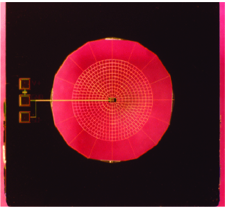
Alternatively to the spider-web absorber, a resonant cavity can be used to maximize the optical efficiency over a limited bandwidth. The SCUBA-2 instrument Duncan et al. (2003); Holland et al. (2003) on the James Clerk Maxwell telescope is an ambitious overtaking with a pixel count of over 12 000. The bolometers consist of thermally isolated, (1 mm2) 60 nm silicon ’bricks’ with the front surface of the Si degenerately doped with phosphorous to 377 per square. The resonant cavity is formed by the Si in between the doped layer, and a Mo-Cu TES deposited to the back side of the pixel.
Even though the superconducting TES thermometers are becoming increasingly popular, bolometers utilizing lithographic semiconducting thermistors still yield impressive performance and are more forgiving in terms of the saturation power. In the so-called pop-up bolometers, a lithographic, doped Si is used as the thermistor, while an ingenious torsional bending method of the Si3N4 legs is used to bend the legs and wiring layers perpendicular to the absorbers. This architecture enables the construction of arrays with a very high filling factor Voellmer et al. (2003). Another promising lithographic resistive thermometer technology is based on thin films of NbSi Camus et al. (2000). The high resistivity of these films allows for impedance levels that provide a good noise matching to room temperature JFET amplifiers.
Instead of the surface absorbing approach, another method is based on the use of a lithographic antenna Hwang et al. (1979); Neikirk et al. (1983), and terminating the induced currents to a thermally isolated bolometer, an approach often used in the HEB mixers discussed above. The attractive feature of this method is that the thermally sensing volume can be made much smaller compared to the case of the surface-absorbing bolometers, making these devices much faster. The low heat capacity often allows for lower NEP, as in many cases the NEPTFN is limited by the maximum time constant allowed by the application. In this case NEP. Moreover, the small size of the thermally sensitive volume makes it far less sensitive to out of band stray light, relaxing filtering and baffling requirements of the incoming radiation. Antenna coupling also lends itself to the construction of integrated, on-chip filters for defining the bands for an array of bolometers Mees et al. (1991); Hunt et al. (2003); Myers et al. (2005). Arrays of antenna-coupled bolometers can also utilize the inherent polarization selectivity of the antennas. An example of an antenna-coupled TES bolometer that incorporates on-chip transmission line impedance transformers and band-pass filters is shown in Fig. 18. No NEPs have yet been measured on this device, but the expected NEP is W for a device with mK.
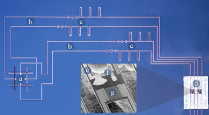
While not published yet, the best performance of an antenna-coupled HPB utilizing a similar design has been obtained by the JPL-Caltech bolometer group, with an electrical NEP= W at 230 mK Kenyon (2005). The architecture is shown in Fig. 19.
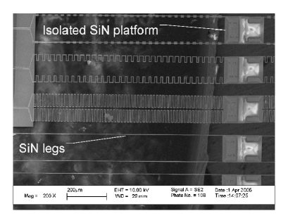
In the simplest case, the bolometer is simply a strip of metal placed to the feed of the lithographic antenna. Although this approach is by far the simplest, it introduces limitations for the performance of a HPB: Unlike in the case of HEB mixers, maximizing the thermal isolation of the bolometer is always desirable. However, the bolometer resistance should be matched to the impedance of the antenna (typically 100 for broadband lithographic antennas on Si substrates), and thus the thermal conductance to the bath through the antenna, , is fixed by the Wiedemann-Franz law, , where is the antenna impedance. A parallel heat loss path is to the substrate below the bolometer film, with conductance where and are the length and width of the bolometer film, respectively. For substrate mounted antenna-coupled HPBs it is thus beneficial to minimize the size of the bolometer. This requirement can be relaxed if the bolometer strip is released from the underlying substrate to form an air-bridge Neikirk and Rutledge (1984). For air-bridged devices at temperatures higher than 4 K, NEP. Recently, an air-bridge bolometer operating at 4.2 K was demonstrated, showing potential for background-limited performance when observing 300 K blackbodies Luukanen and Pekola (2003); Luukanen et al. (2005). The potential applications for these devices include passive detection of concealed weapons under clothing, remote trace detection, and terrestrial submillimetre-wave imaging.
IV.3 Calorimeters: Pulsed excitation
In the limit opposite to the bolometric detection, i.e. when the mean time between the quanta of energy arriving at the detector exceeds the device relaxation time, thermal detectors are known as calorimeters. While the topic of calorimetry also encompasses heat capacity measurements especially in mesoscopic samples, the following discussion concentrates on the detection of radiation only in order to keep the scope of our review in reasonable limits. For those interested in microcalorimetry in the sense of heat capacity measurements, we direct the reader to references Denlinger et al. (1994); Fominaya et al. (1997); Lindell et al. (2000); Bourgeois et al. (2005) and Marnieros et al. (1999).
Cryogenic calorimeters are used today in a large variety of applications, from the detection of weakly interacting massive particles (WIMPs) in dark matter search Akerib et al. (2003); Bravin et al. (1999), X-ray de Korte et al. (2004); Kelley et al. (1999); Moseley et al. (1984) and -ray van den Berg et al. (2000) astrophysics to secure optical communications Miller et al. (2003); Nam et al. (2004). As is the case with bolometers, calorimeters are usually operated at temperatures below 1 K. The theory and operation of calorimetric thermal detectors is very similar to bolometers, and generally the theoretical treatment above is valid. However, the optimization of calorimetric detectors can be quite different. The quantum of energy deposited by either a photon, charged particle, WIMP etc. can be determined from the temperature rise , where is the heat capacity of the calorimeter. This temperature rise then decays exponentially with a time constant to its equilibrium value. Thermometry in the calorimeters is most often done either using semiconducting or TES thermometers, as is the case with bolometers. In addition, thermometry based on the change of magnetization of a paramagnetic sensor is appealing due to its non-dissipative nature, and has yielded some promising results Schönefeld et al. (2000); Fleischmann et al. (2003).
The figure of merit for a calorimeter is the energy resolution, , of full-width at half-maximum (FWHM), related to NEP through Moseley et al. (1984)
| (77) |
For a ’classic’ calorimeter with a white noise spectrum the energy resolution is in terms of the operating temperature and the heat capacity given by
| (78) |
indicating that scales or depending whether the heat capacity of the sensor is dominated by the lattice or the electronic system, respectively.
In most of the devices under development today the lattice temperature is being measured, as sufficient cross section to the incoming energy often requires a rather large volume of a device. An exception to the norm are TES calorimeters optimized for optical single photon detection for applications in secure quantum key distribution Nam et al. (2004), shown in Fig. 20. In these devices, the thermal isolation is via electron-phonon decoupling. A trade-off is made between energy resolution and the speed of the detectors. Energy resolution of the detectors is sufficient to determine the photon-number state of the incoming photons, while maintaining a speed that is adequate for fast information transfer.
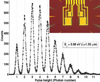
As with bolometers, the TESs currently outperform the competition in terms of the sensitivity. The best reported energy resolution for any energy dispersive detector was recently obtained with a Mo-Cu calorimeter (see Fig. 21), yielding an energy resolution of 2.38 0.11 eV at a photon energy of 5.89 keV Irwin and Hilton (2005).
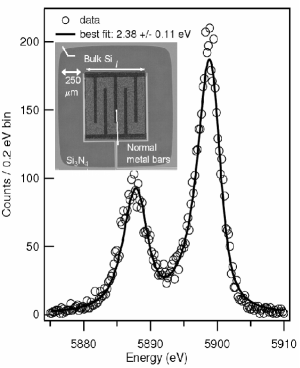
The driving application in the development of X-ray microcalorimeters are two major X-ray astrophysics missions planned by the European Space Agency (ESA) and the U.S. National Astronautics and Space Administration (NASA). Both missions, X-ray Evolving Universe Spectroscopy (XEUS) The European Space Agency (2005) mission and the Constellation-X mission NASA (2005) will employ X-ray microcalorimeters as their primary instrument. The energy resolution of the state of the art microcalorimeters have already reached the requirements stated in the science goals for these missions. Thus, the current primary focus of the technical research is on the development of large arrays of microcalorimeters, and more importantly, SQUID multiplexing read-outs for the detector arrays. A prototype array of Ti/Au TES microcalorimeters is shown in Fig. 22.
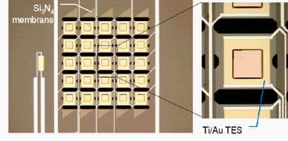
IV.4 Future directions
While cryogenic thermal detectors are the most sensitive radiation detectors around, further significant performance increases are envisioned in the future. The push is from single pixels to large staring focal plane arrays of detectors for numerous astrophysics applications. For this reason, novel thermal detector concepts must be able to be integrated into large arrays.
The performance of hot electron bolometer mixers has been improving rapidly over the past years. Noise temperatures approaching are being reported, and the emphasis is in pushing the operating frequency deeper into the THz region. In principle, frequencies in the infrared range are not out of the question. Lithographic antennas have demonstrated good performance up to 30 THz Grossman et al. (1991), while it is clear that the fabrication becomes increasingly challenging as the required feature size is reduced.
In the single pixel direct detector development, the quest for ever better sensitivity is still ongoing. For bolometers, the improvement in NEP directly translates to the capability of observing over less pre-detection bandwidth without sacrificing signal to noise ratio. This would enable the construction of arrays capable of yielding spectroscopic information. It is here where the functions of HEB mixers, bolometers and calorimeters conjoin - in the capability of performing single photon spectrometry at far-infrared wavelengths.
V Electronic refrigeration
Thermoelectric effects and, in particular, thermoelectric cooling have been discovered more than 170 years ago Peltier (1834). During the last 40 years considerable progress has been made in developing practical thermoelectric refrigerators for industrial and scientific applications Rowe and Bhandari (1983); Nolas et al. (2001). The temperature range of interest has been, however, far above cryogenic temperatures. Yet, during the last decade, solid state refrigerators for low temperature applications and, in particular, operating in the sub-kelvin temperature range have been intensively investigated. The motivations of this activity stem from the successful development and implementation of ultrasensitive radiation sensors and quantum circuits which require on-chip cooling Pekola et al. (2004b) for proper operation at cryogenic temperatures. Solid state refrigerators have typically lower efficiency as compared to more traditional systems (e.g., Joule-Thomson or Stirling gas-based refrigerators). By contrast, they are more reliable, cheaper and, what is more relevant, they can be easily scaled down to mesoscopic scale. All this gives a unique opportunity to combine on-chip refrigeration with different micro- and nanodevices.
The aim of this part of the review is to describe the existing solid state electron refrigerators operating at cryogenic temperatures (in particular below liquid helium temperature), and to give an overview of some novel ideas and refrigeration schemes.
V.1 General principles
The physical principle at the basis of thermoelectric cooling is that energy transfer is associated with quasiparticle electric current, as shown in Sec. II. Under suitable conditions thermal currents can be exploited for heat pumping, and if heat is transferred from a cold region to a hot region of the system, the device acts as a refrigerator. The term refrigeration is associated throughout this Review to a process of lowering the temperature of a system with respect to the ambient temperature, while cooling, in general, means just heat removal from the system. It is noteworthy to mention that the maximum cooling power of a refrigerator is achieved at a vanishing temperature gradient, while the maximum temperature difference is achieved at zero cooling power. The efficiency of a refrigerator is normally characterized by its coefficient of performance (), i.e., the ratio between the refrigerator cooling power () and the total input power ():
| (79) |
Irreversible processes (e.g., thermal conductivity and Joule heating) degrade the efficiency of refrigerators, and are essential elements that need to be carefully evaluated for the optimization of any device.
The basic principles of the design are in general similar for different types of refrigerators. The increase of temperature gradient can be achieved by realizing a multistage refrigerator. In this case, the stage operating at a higher temperature should be designed for larger cooling power in order to efficiently extract the heat released from the lower-temperature stage (”pyramid design”). The enhancement of the refrigerator cooling power can be achieved by connecting several refrigerators in parallel. The parallel design is more effective both for an efficient heat evacuation from the hotter regions of the device and for the application of higher electric currents to the refrigerator. It also allows more freedom to properly bias all cooling elements.
The temperature dependence of the electric and thermal properties of the active parts in the refrigerator may limit their exploitation at low temperatures. The reduction of thermal conductivity by lowering the temperature has both positive (better thermal insulation between cold and hot regions) and negative (difficulty in removing heat from the system) effects.
At cryogenic temperatures different types of superconductors can be efficiently exploited. They can be used both as passive and active elements: in the former case, owing to their low thermal conductivity and zero electric resistance (e.g., as one of the two arms in Peltier refrigerators), in the latter as materials with an energy gap in the density of states for energy-dependent electron tunneling (e.g., in NIS coolers).
Currently, the development of refrigerating techniques follows two main directions: search of new materials with improved characteristics suitable for existing refrigeration schemes, and development of new refrigeration methods and principles.
V.2 Peltier refrigerators
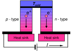
Thermoelectric (Peltier) refrigeration is widely used for cooling different electronic devices Rowe and Bhandari (1983); Nolas et al. (2001); Phelan et al. (2002). Nowadays Peltier refrigerators providing temperature reduction down to K and cooling power up to 100 W are available. Peltier cooling (or heating) occurs when an electric current is driven through the junction of two different materials. The heat released or absorbed, , depending on the direction of the electric current at the junction, is proportional to the electric current () driven through the circuit, , where , and and are the Peltier and Seebeck coefficients of the contact, respectively (see also Eq. (39)). In order to obtain enhanced values of the Peltier coefficient, conventional Peltier refrigerators generally consist of p- and n-type semiconductors with opposite sign of coefficients (see Fig. 23). The efficiency of a Peltier refrigerator is not determined only by the coefficient , but also by thermal conductivities () of both materials across the contact. Furthermore their electric resistances () are responsible of Joule heating affecting the coefficient of performance. The maximum temperature difference () achievable with a Peltier refrigerator is given by Nolas et al. (2001) where is a figure of merit of the refrigerator, and is the temperature of the cold junction (see Fig. 23). More often, however, the refrigerator efficiency is characterized by the dimensionless figure of merit . We recall that . Most of the materials used in thermoelectric applications have at room temperature Min and Rowe (2000); DiSalvo (1999). In general, at low temperatures only one single thermoelectric material is needed, because a superconductor can be used as one of the two arms of the refrigerator Nolas et al. (2001); Goldsmid et al. (1988).
In spite of the drastic reduction of cooling efficiency at low temperature, there is, however, some development of new materials and devices suitable for operation at cryogenic temperatures. Recently, Peltier cooling with K was demonstrated below K Harutyunyan et al. (2003) (see Fig. 24). Crystals of CeB6 were used to exploit the strong thermoelectric coefficients arising from the Kondo effect. The dimensionless figure of merit of this material is in the temperature range between K and K. The authors claim that a proper optimization of the refrigerator design would allow more than 10% temperature reduction below 4K with a single-stage refrigerator.
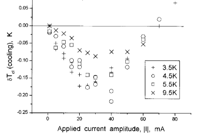
At millikelvin temperatures lattice specific heat and thermal conductivity decrease drastically, and thermoelectric refrigeration might become feasible. Following this idea and taking into account the Wiedemann-Franz relation, values of as high as 20 at temperatures below 10 mK and the possibility to achieve thermoelectric refrigeration were predicted Goldsmid and Gray (1979); Nolas et al. (2001).
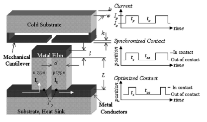
Kapitulnik (1992) proposed to exploit a metal close to its metal-insulator transition for the implementation of a thermoelectric refrigerator operating below liquid-He temperatures. The basic concept behind this proposal is that near the metal-insulator transition, the transport coefficients acquire anomalous power laws such that their relevant combination describing the figure of merit for efficient cooling also becomes large.
Further improvement of the efficiency of conventional thermoelectric coolers could be, in principle, achieved through a thermoelectromechanical refrigerator Miner et al. (1999); Thonhauser et al. (2004). In such a device, a periodic variation of the electric current through a Peltier element combined with a synchronized mechanical thermal switch would allow to improve the overall cooling performance (see Fig. 25). The enhancement of refrigeration is due to the spatial separation of the Peltier cooling and Joule heating.
The analysis of thermoelectric devices is usually based on the parameters typical of bulk materials. Significant progress in low temperature Peltier refrigeration might be achieved by using exotic materials Rontani and Sham (2000); Goltsev et al. (2003) and low-dimensional structures DiSalvo (1999); Hicks et al. (1993); Balandin and Lazarenkova (2003), such as composite thin films, modulation-doped heterostructures, quantum wires, nanotubes, quantum dots, etc. These systems offer, in general, more degrees of freedom to optimize those quantities that affect the efficiency of thermoelectric refrigerators.
V.3 Superconducting electron refrigerators
V.3.1 (SI)NIS structures
Although heat transport in superconducting microstructures originally dates back more than 40 years ago in SIS junctions Parmenter (1961); Melton et al. (1981); Gray (1978); Chi and Clarke (1979), it is instructive to start our description of this topic from NIS tunnel junction structures. Figure 26(a) shows the calculated for a NIS tunnel junction (see Sec. II.G.2) versus bias voltage at different temperatures (). When is positive, it implies heat removal from the N electrode, i.e., hot excitations are transferred to the superconductor. For each temperature there is an optimal voltage that maximizes and, by decreasing the temperature, the heat current results to be peaked around . Figure 26(b) displays the heat current versus temperature calculated at each optimal bias voltage. The quantity is maximized at (as indicated by the arrow in the figure) where it reaches , decreasing both at lower and higher temperatures. Also shown in the figure is obtained assuming a temperature-independent energy gap. Such a comparison shows that this latter assumption is fully justified for . In the low temperature limit () it is possible to give an approximate expression Anghel and Pekola (2001) for the optimal bias voltage (), , as well as for the maximum cooling power at ,
| (80) |
Equation (80) is useful for getting quantitative estimates on the performance of realistic coolers. In the same temperature limit and for the current through the NIS junction can be approximated as . The NIS junction coefficient of performance is given by . For and in the low temperature limit, thus obtains the approximate value
| (81) |
where we assumed , and is the critical temperature of the superconductor. Equation (81) shows that the efficiency of a NIS junction is around or below at the typical operation temperatures. The full behavior of versus temperature calculated at each optimal bias voltage is displayed in Fig. 26(c). The simple results presented above point out how the optimized operation of a superconducting tunnel junction as a building block of microrefrigerators stems from a delicate balance among several factors such as the contact resistance, the operation temperature, the superconducting gap as well as the bias voltage across the junction.
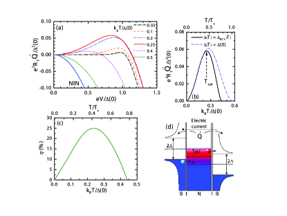
The first observation of heat extraction from a normal metal dates back to 1994 Nahum et al. (1994), where cooling of conduction electrons in Cu below the lattice temperature was demonstrated using an Al/Al2O3/Cu tunnel junction. A significant improvement was made two years later, still in the Al/Al2O3/Cu system, by Leivo et al. (1996), which recognized that using two NIS junctions in series and arranged in a symmetric configuration (i.e., in a SINIS fashion) leads to a much stronger cooling effect. This fact can be understood keeping in mind that is a symmetric function of so that, at fixed voltage across the structure, quasi-electrons above are extracted from the N region through one junction, while at the same time quasi-holes are filled in N below from the other junction (see Fig. 26(d)). In this configuration, a reduction of the electron temperature from mK to about mK was obtained. Later on, several other experimental evidences of electron cooling in SINIS metallic structures were reported Leoni et al. (1999); Fisher et al. (1999); Clark et al. (2004); Arutyunov et al. (2000); Leoni et al. (2003); Tarasov et al. (2003); Pekola et al. (2000a, b); Vystavkin et al. (1999); Fisher et al. (1995); Leivo et al. (1997); Pekola et al. (2004a); Luukanen et al. (2000). In these experiments NIS junctions are used to alter the electron temperature in the N region as well as to measure it. In order to measure the temperature, the N region is normally connected to additional NIS contacts (i.e., ”probe” junctions) acting as thermometers (previously calibrated by varying the bath temperature of the cryostat), and operating along the lines described in Sec. III.A.1. Moreover, the differential conductance of the probe junctions gives also detailed information about the actual quasiparticle distribution function in the N region Pothier et al. (1997b); Pekola et al. (2004a).
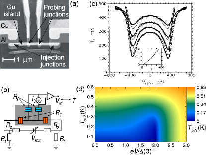
Figure 27(a) shows the SEM micrograph of a typical Al/Al2O3/Cu SINIS refrigerator including the superconducting probe junctions. The schematic of a commonly used experimental setup for electron refrigeration and temperature measurement is shown in Fig. 27(b). The voltage bias across the SINIS structure allows to change the electron temperature in the N region; at the same time, a measure of the voltage drop across the two probe junctions () at a constant bias current () yields the electron temperature in the normal electrode Rowell and Tsui (1976). Figure 27(c) illustrates the experimental data of Leivo et al. (1996) of the measured electron temperature versus , taken at different bath temperatures (i.e., those at ). As can be readily seen, the electron temperature rapidly decreases by increasing the voltage bias across the SINIS structure, reaching the lowest value around eV (note that now two junctions in series are involved in the process). Then, by further increasing the bias, the electron temperature rises due to the heat flux induced into the metal. Furthermore, the minimum electron temperature strongly depends on the starting bath temperature. The inset shows the extracted maximum cooling power (dots) that obtains values as high as pW at mK, corresponding to about 2 pWm2 (in the present experiment, submicron NIS junctions were exploited, with barrier resistances k).
The general operation of a SINIS microrefrigerator like that shown in Fig. 27(a) can be understood by recalling that the final electron temperature in the N region stems from the balance among several factors that tend to drive power into the electron system (i.e., power losses), as discussed in detail in Sec. II. Most of metallic SINIS refrigerators fabricated so far operate in a regime where strong inelastic electron-electron interaction tends to drive the system into quasiequilibrium, where the electron system can be described by a Fermi function at a temperature that differs, in general, from that of the lattice (). At the cryogenic temperatures of interest (i.e., typically below 1 K), the dominant contribution comes from electron-phonon scattering that exchanges energy between electrons and the lattice phonons. The refrigerator cooling power () can be defined as the maximum power load the (SI)NIS device can sustain while keeping the N region at temperature , and can be generally expressed as
| (82) |
where the factor 2 takes into account the presence of two identical NIS junctions, and it is often assumed that in the superconductors . The minimum temperature reached by the N metal thus fulfills the condition . An example of versus behavior along the lines of Eq. (82) is represented by the solid curves plotted in Fig. 27(c). Furthermore, any additional term that adds thermal load into the electron system can be properly taken into account by including its specific contribution to the right-hand side of Eq. (82) Fisher et al. (1999); Ullom and Fisher (2000). Figure 27 (d) shows an example of the calculated electron temperature vs voltage and as obtained from the solution of Eq. (82), . Here we considered a typical Al/Al2O3/Cu SINIS cooler with volume m3, k, nWm3K5 (Cu), and . As it can be readily seen, the value strongly depends on the bias voltage as well as on the lattice temperature. Depending on the thermal load due to the electron-phonon interaction and the operating , the SINIS device can thus behave as a cooler or as a refrigerator.
Let us now highlight some of the basic requirements of SINIS structures for electron cooling operation (their use for lattice cooling is addressed in Sec. V.3.6). In particular, the working temperature range of these structures depends mainly on the type of the superconductor (through its energy gap and hence its critical temperature ), on the strength of the electron-phonon interaction , on the junction resistance , and on the N region volume . First of all, a reduction of the active volume to be cooled is the most straightforward method to increase the efficiency of the refrigeration process, this being more relevant at high lattice temperatures (according to the assumed -dependence of electron-phonon interaction). In addition, cooling power maximization in the high-temperature regime (let us say K) would require both to lower the electron-phonon coupling constant and to increase through a proper choice of the superconductor. The first issue can be solved up to some extent with a variety of materials with different (see Table 1). As far as the second issue is concerned, there is a vast choice of superconducting metals with covering the temperature range up to about K Kittel (1996).
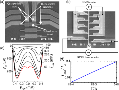
On the other hand, the question of junction resistance requires a careful discussion. In general, from Eq. (80), enhancement is expected from a reduction of . This latter issue can be accomplished both by making thinner barriers and by increasing the junction area. The first issue is not so straightforward, as already discussed in Subs. II.6.2, due to the intrinsic difficulty in fabricating high-quality low- barriers, although optimized barriers are currently under investigation (see Sec. VI.6.1). Latter option was experimentally addressed by Fisher et al. (1999) in Al/Al2O3/Ag refrigerators, where large cooling powers of a few tens of pW were obtained with junctions of m2 surface area. The reduction in electron temperature was, however, much inferior to that achievable with sub-micron sized junction. The problem intrinsic to junctions with large overlap (especially at the lowest temperatures) stems from the larger density of quasiparticles present in the superconductor, due to the fact that quasiparticles require a larger time to exit the junction region and escape from the superconductor. Therefore, this excess of quasiparticles alters in general the refrigerator performance by returning energy to the normal electrode, mainly due to back-tunneling from the superconductor as well as due to recombination processes, where phonons can enter and heat up the N region Ullom and Fisher (2000); Jochum et al. (1998); Kaplan et al. (1976). In addition, inelastic scattering with phonons and dynamic impurities can also lead to an excess of quasiparticles. These contributions can easily overcompensate the junction cooling power, so that it is crucial to remove this excess of quasiparticles from the superconductor. Toward this end a number of techniques exist among which we mention the exploitation of defect-free and thick S electrodes (that allow quasiparticles to escape ballistically from the junction area as well as to decrease their density near the barrier) and the exploitation of quasiparticle ”traps” Parmenter (1961), i.e., normal metal films connected to the superconductor in the junction region through a tunnel barrier or in direct metallic contact Irwin et al. (1995b); Pekola et al. (2000a) (see Fig. 28(a)). Such traps act as sinks of quasiparticles absorbing almost all the excess quasiparticle energy present in the superconductor, and have proved to efficiently help heat removal from the superconductor leading to a significant improvement of SINIS device cooling performance Pekola et al. (2000a, 2004a); Luukanen et al. (2000). All these are commonly exploited tricks for the thermalization of the superconducting electrodes, and in these conditions, it is a reasonable approximation to set . Furthermore, the experiments Pekola et al. (2000a) demonstrated that the trap performance is in general superior when it is in direct metallic contact at short distance from the cooling junction (typically below m, although the optimal distance mainly depends on the superconductor coherence length), nevertheless in small-area junctions even a contact through an insulating barrier seems sufficient for the purpose. The effectiveness of trapping in SINIS structures was theoretically addressed in detail by Voutilainen et al. (2005) and Golubev and Vasenko (2002). Another possibility to achieve high cooling by maximizing the ratio of the junction area to the size of the region to be cooled is to use several small-area junctions (with size in the sub-micron range) connected in parallel to the N electrode (to limit the drawbacks typical of large junctions) Luukanen et al. (2000); Leoni et al. (1999); Arutyunov et al. (2000); Manninen et al. (1999), as shown in Fig. 28(b).
The issue of tunnel junction asymmetry in SINIS refrigerators was addressed by Pekola et al. (2000b). This effect is fortunately weak: these authors theoretically showed that the maximum cooling power is reduced by in the case the junction resistances differ by a factor of two, as compared to a symmetric structure with the same total junction area. Furthermore, the reduction is only about even when the resistance ratio is four. This effect stems from the ”self aligning” character of the double junction structure: the voltage drop across each junction is simultaneously close to , thus corresponding to the maximum cooling power, when the voltage across the whole SINIS system is close to . This fact is due to the high non-linearity of the current-voltage characteristics of the two junctions which carry the same current. The experiments have confirmed such a weak dependence of the cooling power on the structure asymmetry Pekola et al. (2000b).
In the low-temperature regime the situation is rather different. While power load from electron-phonon interaction becomes less and less dominant by decreasing the temperature, and typically below K the cooler behavior can be described as if the lattice would not exist at all, other factors can limit the achievable cooling power as well as the lowest attainable electron temperature. First of all, at the lowest temperatures the maximum achievable cooling power of a NIS junction is intrinsically limited, given by . Then non-idealities in the tunnel barriers, where the possible presence of Andreev-like transport channels (e.g., pin-holes) may strongly degrade the cooling power (in the high temperature regime this contribution is in general overcome by thermal activation) Bardas and Averin (1995). Furthermore, nonequilibrium effects in the N region as well in the S electrodes may be a limitation. In the N region, a suppression of the cooling power is expected by increasing the quasiparticle relaxation time Frank and Krech (1997), i.e., by driving the electron gas far from equilibrium. In the superconductors, a non-thermal distribution can alter the cooling response of the refrigeration process as well as the presence of hot quasiparticle excitations (like with large-area junctions) may be responsible of additional heat load into the N region. Yet, quasiparticle states within the superconducting gap represent a crucial problem at the lowest temperatures, yielding anomalous heating in the N region and limiting the achievable minimum temperature Pekola et al. (2004a). Such quasiparticle states, due mainly to inelastic scattering in the superconductor Dynes et al. (1984) or to inverse proximity effect from the nearby N region, are generally taken into account by adding an imaginary part () to the superconductor DOS, as in Eq. (12). Figure 28(c) shows a representative set of cooling curves taken in an Al/Al2O3/Cu SINIS refrigerator at different lattice temperatures, where at the lowest temperature (red dash-dotted line) (this typically happens around or below mK) the electron gas first undergoes heating, then it is strongly cooled at the expected bias around . A similar anomaly was reported in some experiments on SINIS refrigerators Pekola et al. (2004a); Fisher et al. (1999); Savin et al. (2001); Pekola et al. (2000b). The anomalous heating was attributed to the presence of such states within the S gap that give rise to a sort of dissipative channel which dominates heat current in a certain bias range Pekola et al. (2004a). Pekola et al. (2004a) theoretically demonstrated that the minimum achievable electron temperature () in SINIS refrigerators is set by the amount of quasiparticle states present within the superconducting gap, and is given by at in quasiequilibrium (see Fig. 28(d)). We note that a measure of the value in real NIS junctions is approximately given by the ratio of the zero-bias to the normal state junction conductance at low temperature. The existence of quasiparticle states within the superconducting gap thus sets a fundamental limit to the minimum achievable temperature, and great care has to be devoted to get rid of their presence to optimize the refrigeration process at the lowest temperatures.
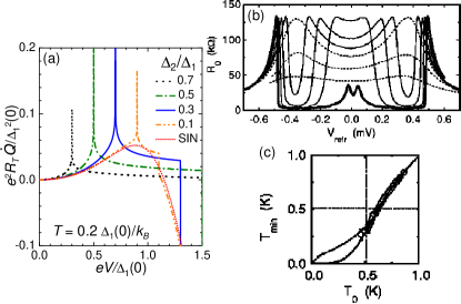
V.3.2 S1IS2(IS1) structures
The enhancement of superconductivity by quasiparticles extraction was proposed in 1961 by Parmenter (1961) in the context of S1IS2 tunnel junctions, where S1 and S2 represent superconductors with different energy gaps. Later on, Melton et al. (1981) theoretically discussed the possibility to exploit such a system to realize a refrigerator (addressing both the basic features and performance). From an experimental point of view, Chi and Clarke (1979) observed in Al films an enhancement of the energy gap of the order of 40 due to quasiparticle extraction. Then, Blamire et al. (1991), using Nb/AlOx/Al/AlOx/Nb structures, were able to obtain an enhancement of the critical temperature of the Al layer by more than . The physical mechanism giving rise to this effect was discussed by Heslinga and Klapwijk (1993) and by Zaitsev (1992). More recently, also Nevirkovets (1997) observed in similar structures an enhancement of the Al gap by quasiparticle extraction.
Figure 29(a) shows the calculated heat current versus bias voltage for a S1IS2 tunnel junction at for various ratios (see Eq. (30)). The quantity is an even function of , thus allowing connection of two junctions in a symmetric configuration as in the NIS case, and is positive for where hot quasiparticle excitations are removed from S2. Moreover, the heat current is maximized at , where it is logarithmically diverging Tinkham (1996); Harris (1974) (note that this is somewhat broadened by the smearing in the density of states in a realistic situation Manninen et al. (1999); Pekola et al. (2004a); Frank and Krech (1997)). From Fig. 29(a) it follows that heat extraction from S2 only occurs if holds. Then, at a sharp transition brings to negative values (more details about the heat transport in S1IS2 junctions can be found in Frank and Krech (1997)). The dotted line represents when the electrode S2 is in the normal state (i.e., NIS case). Notably, when both electrodes are in the superconducting state, can exceed significantly that in the normal state. This peculiar characteristic of heat transport in S1IS2 junctions makes them promising in realizing a ”cascade” refrigerator that might operate at bath temperatures higher than those for a SINIS cooler, where several combined superconducting stages are used to efficiently cool a normal or a superconducting region.
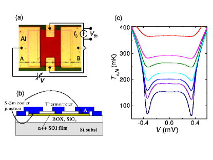
The experimental observation of electron cooling in a superconductor was reported by Manninen et al. (1999) using Al/insulator/Ti tunnel junctions. In this experiment, aluminum (i.e, the larger-gap superconductor) was used to cool the electron system of a Ti strip from to below , where K was the Ti critical temperature. Figure 29(b) shows a representative set of measurements taken at different bath temperatures . In particular, it shows the zero-bias resistance of the thermometer junctions against the bias voltage across the refrigerators (). Dashed lines indicate the behavior at bath temperatures where Ti is still in the normal state: the electron temperature in Ti decreases (i.e., increases) by increasing , reaching a minimum slightly below eV, as expected for a SINIS refrigerator ( is the energy gap of Al). Note that dashed lines are the upside-down equivalent, for example, of the measurements shown in Fig. 27(c). Thin solid lines indicate the temperature behavior when Ti is cooled from the normal to the superconducting state. This happens for larger than but below 625 mK, at values for which has a deep minimum. Here, for instance, starting from mK, the minimum electron temperature reached in Ti was mK, thus demonstrating the effectiveness of the cooling mechanism also in all-superconducting refrigerators. Thick solid line corresponds to the case where the Ti strip is already superconducting, i.e., at a bath temperature below . The results for the minimum electron temperature reached in Ti against is represented by the open circles in Fig. 29(c). Comparison to the theory gave good agreement with the experiment (lines in Fig. 29(c)) with an electron-phonon interaction constant nWm3K5.
V.3.3 SSmS structures
Superconductor-semiconductor structures have recently attracted interest in the field of electron cooling Savin et al. (2001); Buonomo et al. (2003); Savin et al. (2003). The basic idea is to exploit, for the active part of the cooler, heavily-doped semiconductor layers instead of normal metals, with the natural Schottky barrier forming at the contact to the metal electrodes Brennan (1999); Lüth (2001); Rhoderick and Williams (1988); Sze (1985, 1981). The peculiar characteristic intrinsic to this scheme stems from the possibility to alter up to a large extent the semiconductor electronic properties (like, for example, the charge density, etc.) and to change the transmissivity of the Schottky barrier through proper doping or choice of the semiconducting layer (see also Sec. VI.F.2).
Heavily-doped silicon is a natural choice both from a practical and technological point of view, mainly owing to the widespread and well-developed Si technology. Up to now, the only evidence of superconducting electron cooling with semiconductors comes from microrefrigerators realized with the silicon-on-insulator (SOI) technology Savin et al. (2001); Buonomo et al. (2003); Savin et al. (2003). The first demonstration of electron refrigeration in Si was reported by Savin et al. (2001), where the authors obtained a maximum temperature reduction under hot quasiparticle extraction of the order of at the bath temperature mK. Figure 30(a) shows the optical micrograph of a typical Al/Si/Al cooler. The two bigger Al electrodes are used for cooling, while the two smaller for detecting the electronic temperature in Si. A sketch of the structure cross-section is displayed in Fig. 30(b), where the -Si region appears just on top of the silicon dioxide insulating layer. The structures were characterized by a doping level cm-3. A set of cooling curves extracted from one of such devices is shown in Fig. 30(c) Savin et al. (2003). It displays the electron temperature in the -SOI layer versus bias voltage across the refrigerator at different starting bath temperatures. The observed electronic temperature reduction is of the order of at mK. Although the device volume and the cooler resistances were rather high, the authors attributed this significant cooling to a very small electron-phonon coupling constant in Si: as a matter of fact, the latter was determined to be nWm3K5 Savin et al. (2001), i.e., about one order of magnitude smaller than in Cu. The maximum achieved cooling power was pW at mK, mainly limited by the high value of the specific contact resistances ( km2). These authors also addressed the effect of carrier concentration in Si on cooling performance Savin et al. (2003).
Buonomo et al. Buonomo et al. (2003) also obtained a cooling effect in Al/Si/Al refrigerators, with a device configuration similar to that of Fig. 30(a). Their structures were characterized by a doping level cm-3 and contact specific resistances km2. Notably, they confirmed the same value reported by Savin et al. (2001) for the electron-phonon coupling constant in Si. In addition, these authors also explored the Nb/Si/Nb combination for electron cooling. Their results, however, showed no cooling effect, owing probably to a too transmissive interface at the contact with Si. This effect was ascribed both to the slightly lower Schottky barrier height of Nb/Si contact ( eV Heslinga and Klapwijk (1989); Chang et al. (1971)) with respect to the Al/Si ( eV Chang et al. (1971); Singh (1994)) and to disorder-enhanced subgap conductance Badolato et al. (2000); Kastalsky et al. (1991); van Wees et al. (1992); Giazotto et al. (2001a, b); Nguyen et al. (1992); Nitta et al. (1994); Xiong et al. (1993); Poirier et al. (1997); Kutchinsky et al. (1997); Magnée et al. (1994); Bakker et al. (1994); Giazotto et al. (2003a). Further results on the electron-phonon coupling constant as well as on the electronic thermal conductivity in -type Si were reported in Kivinen et al. (2003); Heslinga and Klapwijk (1992).
Because of the low electron-phonon coupling constant in heavily doped Si, one may expect to cool islands with larger volumes than in the normal metal case, and perhaps improve the high-temperature limit of cooling by some factor. The issue of high values that limit the maximum achievable cooling power still represents a drawback of these refrigerators that has to be overcome. High doping of the semiconductor (in the tunneling regime Sze (1985, 1981), see also Sec. VI.F.2) as well as engineering of the Schottky barrier height through incorporation of interface layers at the metal-semiconductor junction De Franceschi et al. (2000, 1998b, 1998a); Grant and Waldrop (1988); Costa et al. (1991); Koyanagi et al. (1993); Cantile et al. (1994b, a); Marinelli et al. (2000) can be exploited in order to tailor the interface transmissivity.
V.3.4 SF systems
As discussed at the beginning of Sec. V.3.1, decreasing the contact resistance () is not a viable route to enhance heat current in NIS junctions. A possible scheme to surmount the problem of Andreev reflection at the metal-superconductor interface is to exploit, instead of an insulating barrier, a thin ferromagnetic (F) layer in good electric contact with S Giazotto et al. (2002). The physical origin of the SF cooler operation stems from the spin-band splitting characteristic of a ferromagnet. The electron involved in the Andreev reflection and its phase-matched hole belong to opposite spin bands; as a consequence, depending on the degree of spin polarization of the F layer, strong suppression of the Andreev current may occur at the SF interface de Jong and Beenakker (1995). In the limit of large , the subgap current is thus strongly suppressed while efficient hot-carrier transfer leads to a sizeable heat current across the system. In the following we give the main results of such a proposal.
The impact of partial spin polarization () in the F region is displayed in Fig. 31(a) where the heat current versus bias voltage across the junction is plotted for some values of at ( is the electron temperature in F). For each value there exists an optimum bias voltage () which maximizes . In the limit of a half-metal ferromagnet (i.e., ) Mazin (1999); Coey and Sanvito (2004) this value is around . Moreover, for there is still a positive across the junction. The inset of Fig. 31 (a) shows calculated at each optimized bias voltage against temperature for various values of . The heat current is maximized around , rapidly decreasing both at higher and lower temperatures.
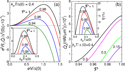
The junction specific cooling power is shown in Fig. 31(b), where (evaluated at each optimal bias voltage) is plotted versus at different bath temperatures. Notably, for a half-metallic ferromagnet at , cooling power surface densities as high as nW/m2 can be achieved, i.e., about a factor of 30 larger than those achievable in NIS junctions at the optimized interface transmissivity (i.e., at , see Fig. 4(b)). This marked difference stems from SF specific normal-state contact resistances as low as some m2 that are currently achieved in highly-transmissive junctions Upadhyay et al. (1998). The inset of Fig. 31(b) shows the junction coefficient of performance () calculated at the optimal bias voltage versus temperature for various values. Notably, for , reaches around and exceeds for . In addition, in light of a possible exploitation of this structure in combination with a N region (i.e., a SFN refrigerator) it turned out that cooling effects comparable to the SF case can be achieved with a F-layer thickness of a few nm (i.e., of the order of the magnetic lenght). We note that the large typical of the SF combination makes it promising as a possible higher-temperature first stage in cascade cooling (for instance, over or around 1 K), where it could dominate over the large thermal coupling to the lattice characteristic for such temperatures.
The results given above point out the necessity of strongly spin-polarized ferromagnets for a proper operation of the SF refrigerator. Among the predicted half-metallic candidates it is possible to indicate CrO2 Kämper et al. (1987); Brener et al. (2000); Schwartz (1986), for which values of in the range have been reported Ji et al. (2001); Parker et al. (2002); Dedkov et al. (2002); Coey et al. (1998), (Co1-xFeS2 Mazin (2000), NiMnSb de Groot et al. (1983), Sr2FeMoO6 Kobayashi et al. (1998) and NiMnV2 Weht and Pickett (1999). So far no experimental realizations of SF structures for cooling applications have been reported.
V.3.5 HTc NIS systems
Heat transport in high-critical temperature (HTc) NIS junctions was theoretically addressed by Devyatov et al. (2000). In these systems the cooling power depends on interface transmissivity as well as on orientation of the superconductor crystal axes and temperature. In particular, these authors showed that the maximum positive heat current in these structures can be achieved in junctions with zero superconducting crystallographic angle, at temperature and bias voltage . The behavior of turns out to be qualitatively similar to that of NIS junctions based on low-critical temperature superconductors (see Fig. 26(a)), and with comparable values (in relative units). From this it follows that the cooling power of electronic refrigerators based on HTc materials is approximately two orders of magnitude larger than in NIS junctions based on low-critical temperature superconductors (at much lower temperatures).
A somewhat different cooling effect in HTc superconductors was predicted by Svidzinsky (2002), who showed that an adiabatic increase of the supercurrent in a ring (or cylinder) made from a HTc superconductor may lead to a cooling effect. The maximum cooling occurs if the supercurrent is equal to its critical value. For a clean HTc superconductor, the minimum achievable temperature () was found to be around , with the initial temperature of the ring, thus meaning that substantial cooling can be achieved using large values.
Experimentally, Fee (1993) realized a Peltier refrigerator junction exploiting a HTc superconductor and operating around liquid nitrogen temperatures. In particular, his device consisted of a BiSb alloy and YBa2Cu3O7-δ superconducting rods connected by a small copper plate which acted as the cold junction of the device. The latter showed a maximum cooling of K below the bath temperature K. The figure of merit of the junction, , was estimated to be as large as K-1.
V.3.6 Application of (SI)NIS structures to lattice refrigeration
One well established application of SINIS refrigerators concerns lattice cooling Manninen et al. (1997); Luukanen et al. (2000); Clark et al. (2005). As a matter of fact, while NIS tunneling directly cools the electron gas of the normal electrode, the phonon system can be refrigerated through the electron-phonon coupling (see Eq. (24)). The latter, however, is typically very small at the lowest temperatures, thus limiting the heat transfer from the surroundings to the electrons. This situation normally happens whenever the metal to be cooled is in direct contact with a thick substrate, for instance, oxidized Si Nahum et al. (1994); Leivo et al. (1996): only the electrons of the N region cool down while the metal lattice presumably remains at the substrate temperature. The metal lattice can be refrigerated considerably if the thermal resistance between the phonons and the substrate is not negligible compared to that between the electrons and the phonons. One effective choice to meet this requirement, that was indeed suggested at the beginning of cooling experiments Nahum et al. (1994); Fisher et al. (1995) as well as for detector applications Irwin et al. (1996); Nahum and Martinis (1995); Doriese et al. (2004); Ullom et al. (2004); Deiker et al. (2004); Pekola et al. (2004b), is to exploit a thermally isolated thin dielectric membrane on which the N region of the cooler is extended. In this way, tunneling through the NIS junction will cool down the electrons of the metal, then the phonons of the metal (via electron-phonon coupling) that subsequently will refrigerate the membrane phonons Manninen et al. (1997); Luukanen et al. (2000); Clark et al. (2005) according to
| (83) |
where , , is the lattice temperature in the dielectric membrane, is the lattice temperature in the substrate, and is the rate of exchanged energy between the membrane phonons and substrate phonons. Eventually, if additional devices are standing on the same dielectric platform (for instance, detectors, etc.), the latter will cool down first the phonons of the device and then its electrons through the electron-phonon interaction.
Dielectric membranes made of silicon nitride (Si3N4) have proved to be attractive for this purpose in light of their superior thermal isolation properties at low temperatures. Low-temperature heat transport characterization as well as thermal relaxation in low-stress Si3N4 membranes and films were quite recently addressed Leivo and Pekola (1998); Holmes et al. (1998). The first demonstration reported of lattice cooling Manninen et al. (1997) exploited such membranes in combination with Al/Al2O3/Cu SINIS refrigerators. In this experiment the authors were able to achieve a temperature decrease in the membrane at bath temperatures mK.
Figure 32(a) shows a SEM image of a typical new-generation lattice cooler fabricated on a Si3N4 membrane with self-suspended bridges. The membrane consists of a low-stress Si3N4 film deposited by low pressure chemical vapor deposition (LPCVD) on Si, and subsequently etched (with both wet and dry etching) in order to create the suspended bridge structure. In such thin membranes phonon propagation is essentially two-dimensional. The condensation of the phonon gas into lower dimensions in ultrathin membranes was also theoretically discussed Anghel et al. (1998); Anghel and Manninen (1999); Kuhn et al. (2004). The self-suspended bridges improve thermal isolation of the dielectric platform from the heat bath Leivo and Pekola (1998). The image also shows the Al/Al2O3/Cu refrigerators of the SINIS type that are placed on the bulk substrate (i.e., outside the membrane) to ensure good thermal contact with the bath. The N cold fingers extend onto the silicon nitride membrane, whose temperature is determined through an additional SINIS thermometer placed in the middle of the structure.
The lattice refrigeration effect achieved in this SINIS refrigerator is shown in Fig. 32(b). Here the maximum temperature decrease of the membrane () against bath temperature is displayed (red circles), and shows that temperature reduction as high as about was reached in the mK range. The electron refrigeration effect in the Cu region was also measured at two different positions in the device, i.e., nearby the cooling junctions and on the membrane. Notably, the behavior is almost the same for the different sets of data; this basically means that: a) good thermalization was achieved in the cold fingers; b) the electron-phonon coupling was sufficiently large while Kapitza resistance between Cu and Si3N4 was sufficiently small to ensure the lattice temperature on the membrane to be nearly equal to the Cu electron temperature on the membrane itself. The best results of lattice refrigeration by SINIS coolers reported to date are shown in Fig. 32(c) Luukanen et al. (2000) for two other devices (labeled C and D in the figure) similar to that of Fig. 32(a). These devices exploited three Cu cold fingers and several small-area junctions arranged in parallel in a comb-like configuration for the SINIS cooling stage. The junction specific resistances were km2 and m2 for device C and D, respectively. Lattice temperature reduction as high as at 200 mK was achieved in the sample with lower , thus confirming the effectiveness of small-area junctions in yielding larger temperature reductions. The achieved cooling power in these devices was estimated on the pW level. The reduction of the refrigeration effect at the lowest temperatures can be explained in terms of larger decoupling of electrons and phonons, but also the effects discussed in Sec. V.3.1 should play a role.
Figure 32 (d) demonstrates the realization of a complete refrigerator device including a thermometer Clark et al. (2005), where four pairs of NIS junctions are used to cool down a m2 suspended Si3N4 dielectric membrane. Each NIS junction area is m2, and the N electrode consists of Al doped with Mn to suppress superconductivity while Al is used for the superconducting reservoirs. Also shown is a neutron transmutation doped (NTD) Ge resistance thermometer (with volume m3) glued on the membrane. In such a refrigerator the authors measured with the NTD Ge sensor a minimum final temperature slightly below mK starting from a bath temperature mK, under optimal bias voltage across the cooling junctions. This result is promising in light of a realistic implementation of superconducting refrigerators, and shows the possibility of cooling efficiently the whole content of dielectric membranes through NIS junctions Pekola (2005).
Possible strategies to attain enhanced lattice refrigeration performance in the low temperature regime (i.e., below 500 mK) could be a careful optimization in terms of the number and specific resistance of the cooling junctions as well as to exploit superconductors with the gap larger than in Al. Making the dielectric platform thinner and reducing thermal conduction along it should also increase the temperature drop across the membrane. The exploitation of the described method around or above 1 K, however, is still now not so straightforward, mainly due to the strong temperature dependence of the electron-phonon interaction that thermally shunts more effectively the N electrode portion standing on the bulk substrate to the lattice (note that also the thermal conduction along the membrane is strongly temperature dependent Leivo and Pekola (1998); Kuhn et al. (2004)). Toward this end, a reduction of the N volume placed out of the membrane should help; in addition, S1IS2(IS1) refrigerators (see Sec. V.3.2) as well as SF junctions (see Sec. V.3.4) might significantly improve the membrane cooling in the higher temperature regime.
V.3.7 Josephson transistors
A further interesting field of application of SINIS structures concerns superconducting weak links Likharev (1979); Golubov et al. (2004). In particular, in diffusive SNS junctions, i.e., where the junction length largely exceeds the elastic mean free path, coherent sequential Andreev scattering between the superconducting electrodes may give rise to a continuum spectrum of resonant levels Heikkilä et al. (2002); Belzig et al. (1999); Yip (1998) responsible for carrying the Josephson current across the structure. The supercurrent turns out to be given by this spectrum weighted by the occupation number of correlated electron-hole pairs, the latter being determined by the quasiparticle energy distribution in the N region of the weak link. In controllable Josephson junctions, the supercurrent is modulated by driving the quasiparticle distribution out of equilibrium van Wees et al. (1991); Wilhelm et al. (1998); Yip (1998); Heikkilä et al. (2002); Volkov (1995); Seviour and Volkov (2000a); Volkov and Pavlovskii (1996); Volkov and Takayanagi (1997) via dissipative current injection in the weak link from additional normal-metal terminals. This operation principle leads to a controlled supercurrent suppression and was successfully exploited both in all-metal Morpurgo et al. (1998); Baselmans et al. (1999); Shaikhaidarov et al. (2000); Huang et al. (2002); Baselmans et al. (2002a, b, 2001a, 2001b) (where a transition to a -state was also reported) as well as in hybrid semiconductor-superconductor weak links Kutchinsky et al. (1999); Schäpers et al. (1998); Neurohr et al. (1999); Schäpers et al. (2003b, a); Richter (2000). The situation drastically changes if we allow current injection from additional superconducting terminals arranged in a SINIS fashion Baselmans (2002); Giazotto et al. (2003b, 2004b, 2004a). In this way, thanks to the SINIS junctions, critical supercurrent can be strongly increased as well as steeply suppressed with respect to equilibrium, leading to a tunable structure with large current and power gain.
A simplified scheme of this class of transistors is displayed in Fig. 33(a). A diffusive SJNSJ long Josephson junction of length (i.e., with , where is the coherence length) shares the N region of a SINIS control line of length . The superconductors SJ and S can be in general different (i.e., with gaps and , respectively); in addition, the SJ electrodes are kept at zero potential, while the SINIS line is biased with . The supercurrent () behavior in response to a bias voltage stems from the degree of nonequilibrium the SINIS line is able to generate in the weak link according to Wilhelm et al. (1998); Yip (1998); Heikkilä et al. (2002)
| (84) |
where is the weak link normal-state resistance, is the phase difference across the superconductors, and is the spectral supercurrent, obtainable from the solution of the Usadel equations Usadel (1970). The most straightforward situation occurs at sufficiently low lattice temperatures, i.e., typically below K, when (see Sec. II). In such a case, strong electron-electron relaxation forces the electron system in the N region to retain a local thermal quasiequilibrium (see also Sec. V.3.1), so that . The transistor effect in the structure thus simply depends on the electron temperature established in the weak link upon biasing the SINIS line according to Eq. (82). The full calculation of the behavior of a prototype Nb/Cu/Nb long Josephson junction with integrated Al/Al2O3/Cu SINIS electron cooler is displayed in Fig. 33(b) Giazotto et al. (2003b). Here the normalized is plotted against for several bath temperatures . For all chosen values of , the supercurrent value increases monotonically up to about , where the SINIS line provides the largest cooling power and allows to attain the lowest electron temperature. Then, by further increasing the voltage, an efficient suppression of occurs due to electron heating: the device behaves as a tunable superconducting junction. The above given results can be easily understood recalling that for a long SNS junction at low lattice temperature (i.e., ) and for ( is the N-region diffusion coefficient), depends exponentially on the effective electron temperature Zaikin and Zharkov (1981); Wilhelm et al. (1997) and is almost independent of . Hence, long junctions are more appropriate for the device to obtain large changes with small variations (as indicated by the red hatched region in the inset of Fig. 33(b)). In the short junction limit (), conversely, the temperature dependence is set by the energy gap , thus implying a much reduced effect from the cooling line. Furthermore, it is expected that the power dissipation values from two to four order of magnitude smaller than with all-normal control lines can be obtained in these structures, thus making them promising as mesoscopic transistors for low dissipation cryogenic applications.
So far, the only successful demonstration of this transistor-like operation was reported by Savin et al. (2004) in Al/Cu/Al SNS junctions integrated with Al/Al2O3/Cu SINIS refrigerators. The SEM image of one of these samples along with a scheme of the measurement setup is shown in Fig. 33(c). The structure parameters were the following: cooler junction resistances , Josephson weak link normal state resistance , and minimum SNS interelectrode separation m that compared with the superconducting coherence length ( nm) provides the frame of the long junction regime. The critical current versus at three different is shown in Fig. 33(d). For each bath temperature, increases around , as expected from the reduction of by electron cooling, while it is steeply suppressed at larger bias voltages. The resemblance of the experiment with the curves of Fig. 33(b) is evident. In the present case, enhancement under hot quasiparticle extraction by more than a factor of two was observed at mK. The transistor current gain , shown in the inset of Fig. 33(d), obtained values in the range depending on the control bias. As far as power dissipation is concerned, these authors reported low dissipated power on the W level in the extraction regime while of some tens of pW in the regime of suppression.
The transistor behavior for arbitrary inelastic scattering strength in the SINIS line (or, equivalently, for arbitrary values of ) as well as for different SNS junction lengths, was theoretically addressed in detail in Giazotto et al. (2004b, a). The role of geometry, materials combination, phase dependence, and the input noise power were also discussed. Notably, a marked supercurrent transition to a -state under nonequilibrium (about two times larger than that achievable with an all-normal control channel Wilhelm et al. (1998); Yip (1998)) was predicted to occur for negligible or moderate electron-electron interaction. We recall that in the -state Bulaevskii et al. (1977) the supercurrent flows in opposite direction with respect to the phase difference between the two superconductors, i.e., such a sign reversal is equivalent to the addition of a phase factor to the Josephson current-phase relation. Furthermore, current gain in the range and power gain up to where predicted to occur depending on the control voltage.
Finally, transistor operation in a Josephson tunnel junction integrated with a S1IS2IS1 refrigerator was also theoretically addressed in the quasiequilibrium regime Giazotto and Pekola (2005). In this case, the device benefits from the sharp characteristics due to the presence of superconductors with unequal energy gaps (see also V.3.2), that leads to improved overall characteristics as compared to the SINIS-controlled SNS junction in the same transport regime.
V.4 Perspective types of refrigerators
Any electric current that is accompanied by the extraction of hot electrons (or holes) can be used, in principle, for refrigeration purposes. For instance, this may happen in thermionic transport over a potential barrier as well as in energy-dependent tunneling through a barrier. Since an exhaustive analysis of all possible predicted refrigeration methods is far beyond the limits set to this Review, in the following we give a brief description of a few examples that we believe are relevant in the present context. In such devices, several different effects may contribute to the refrigeration process (e.g., thermionic transport, quantum tunneling as well as thermoelectric effects), so that making a proper ”classification” of the refrigeration principle is, strictly speaking, rather difficult. As a consequence, we shall try mainly to follow the definitions as they were introduced in the original literature.
V.4.1 Thermionic refrigerators
A vacuum thermionic cooling device consists of two electrodes separated by a vacuum gap. Cooling occurs when highly energetic electrons overcome the vacuum barrier through thermionic emission, thus reducing the electron temperature of one of the two electrodes. In such a situation, the refrigerator operation is mainly affected and limited by radiative heat transfer between the electrodes. The thermionic emission current density () is given by the Richardson equation, , where and are the work function and the temperature of the emitting electrode, respectively, is the Richardson constant, and is the electron mass. From the expression above, a strong reduction of is expected upon lowering the temperature. Mahan (1994) developed a simple model for thermionic refrigeration, and demonstrated that its efficiency can be as high as 80% of the Carnot value. Vacuum thermionic refrigerators are generally characterized by a higher efficiency as compared to thermoelectric coolers, and are considered to be an attractive solution for future refrigeration devices Nolas and Goldsmid (1999). However, the high values typical of currently available materials make thermionic cooling efficient, at present, only above 500 K.
Several ideas on how to increase the cathode emission current and to improve the operation of these refrigerators have been proposed Korotkov and Likharev (1999); Hishinuma et al. (2002, 2001); Purcell et al. (1994). Korotkov and Likharev suggested to cover the emitter with a thin layer of a wide-gap semiconductor, and to exploit the resonant emission current to cool the emitter Korotkov and Likharev (1999). The analysis of such a thermionic cooler predicted an efficient refrigeration down to 10 K.
The issue of high values can be overcome by a reduction of the distance between the electrodes (in the submicron range) and by the application of a strong electric field. Following this scheme, Hishinuma et al. (2001) theoretically analyzed a thermionic cooler where the two electrodes where separated by a distance in the nanometer range. In such a situation, the potential barrier is essentially lowered (see Fig. 34(a)), allowing both thermionic emission and energy-dependent tunneling. As a consequence, rather small (if compared to vacuum thermionic devices) external voltages ( V) are required in order to produce significant electric currents. For suitable values of the applied voltage and distances between the electrodes, electrons above the Fermi level dominate the electric transport (both thermionic emission over the barrier and tunneling through the barrier), thus leading to cooling of the emitter. As it can be inferred from Fig. 34(b), the contribution of the energy-dependent tunneling to total cooling is essential, and this refrigerator could be classified as a vacuum tunneling device. The cooling power surface density in this combined thermionic-tunneling refrigerator was predicted to obtain values as high as 100 W/cm2 at room temperature. However, in the only experimental demonstration of this device, a moderate emission current (below 10 nA) was reported at room temperature, with an observed temperature reduction of about 1 mK Hishinuma et al. (2003). So far, no experimental demonstration of vacuum thermionic refrigeration at cryogenic temperatures has been reported.
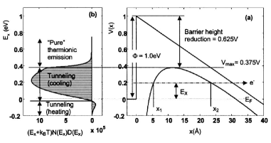
V.4.2 Application of low-dimensional systems to electronic refrigeration
The exploitation of low-dimensional systems gives additional degrees of freedom in order to engineer materials that may lead to enhanced operation of thermoelectric and thermionic devices Sales (2002); Hicks et al. (1993); Hishinuma et al. (2002); Sofo and Mahan (1994). Some of the limitations intrinsic to vacuum thermionic refrigerators can be overcome with solid state thermionic coolers Shakouri and Bowers (1997); Mahan and Woods (1998). As a matter of fact, modern growth techniques easily allow one to control both the barrier height and its width within a wide range of values. One disadvantage of solid state thermionic coolers stems from the thermal conductivity of the barrier which is essentially absent in vacuum devices. Nevertheless, a large temperature reduction can be achieved by using a multilayered heterostructure Shakouri and Bowers (1997); Mahan and Woods (1998); Zhou et al. (1999). According to theory Shakouri and Bowers (1997); Mahan and Woods (1998), heterostructure-based thermionic refrigerators perform somewhat better as compared to thermoelectric coolers. The predicted temperature reduction of a single-stage device at room temperature can be as high as 40 K, and this value can be significantly increased in a multilayer configuration. So far, however, the experimental implementations of single barrier Shakouri et al. (1999) and superlattice Fan et al. (2001); Zhang et al. (2003) refrigerators have reported temperature reductions of a few degrees at room temperature.
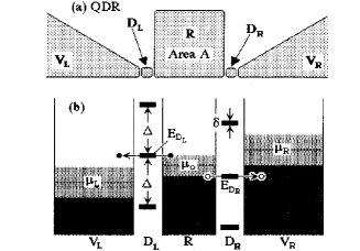
Further improvement of thermionic refrigeration can, in principle, be achieved by combining laser cooling and thermionic cooling Shakouri and Bowers (1997); Mal’shukov and Chao (2001). In such an opto-thermionic device, hot electrons and holes extracted through thermionic emission lose their energy by emitting photons rather than by heating the lattice. The theoretical investigation of a GaAs/AlGaAs-based opto-thermionic refrigerator predicted specific cooling power densities of the order of several W/cm2 at K Mal’shukov and Chao (2001).
The presence of singularities in the energy spectrum of low-dimensional systems can be used in solid state refrigeration. For instance, the discrete energy spectrum in quantum dots can be exploited for refrigeration at cryogenic temperatures Edwards et al. (1993, 1995). In such a quantum-dot refrigerator (QDR) (see Fig. 35(a)) a reservoir (R) is coupled to two electrodes via quantum dots (D and D) whose energy levels can be tuned through capacitively-coupled electrodes. The QD energy levels can be adjusted so that resonant tunneling to the electrode V is used to deplete the states in R above and, similarly, holes below in R tunnel to V (see Fig. 35(b)). As a consequence, the net result will be to sharpen the quasiparticle distribution function in R, thus leading to electron refrigeration. In spite of a rather moderate achievable cooling power, the QDR was predicted to be effective for cooling electrons of a micrometer-sized two-dimensional electron gas reservoir at mK temperatures, and even of a macroscopic reservoir at lower temperatures Edwards et al. (1993, 1995).
VI Device fabrication
VI.1 Structure typologies and material considerations
This section is devoted to the description of the main techniques and experimental procedures used for the fabrication of typical superconducting electronic refrigerators and detectors. Owing to the great advances reached in the last decades in micro- and nanofabrication technology Timp (1999); Bhushan (2004), the amount of information related to fabrication methods is too large to be covered here and beyond the scope of the present review. Therefore, we only briefly highlight all those issues that we believe are strictly relevant for this research field. In particular we first of all focus on the two typologies of existing superconducting structures, namely all-metal and hybrid devices, and on the main differences between them, both in terms of materials and fabrication techniques. The former concern structures where the active parts of the device, i.e., both the superconducting elements and the normal regions are made of metals; in hybrid structures, the non superconducting active part of the device is made of doped semiconducting layers.
As far as all-metal-based structures are concerned, they are realized with low-critical-temperature thin-film superconductors (normally Al, Nb, Ti and Mo), while the normal regions usually consist of Cu, Ag or Au. Their fabrication protocol includes patterning of a suitable radiation-sensitive masking layer through electron-beam or optical lithography in combination with a shadow-mask (angle) evaporation technique Dolan (1977). The final device is thus realized in a single step in the deposition chamber, where additional tunnel barriers between different regions of the structure are in-situ created by suitable oxidation of the metallic layers. Although all this leads to an efficient way for fabricating metallic structures, however the electronic properties typical of metals are only weakly dependent on their growth conditions and on the specific employed technique. As a consequence, it is hard to tailor the metallic properties in order to finally match some specific requirements.
On the other hand, the situation is rather different with semiconductors that offer some advantages in comparison to metals. The large magnitude difference of Fermi wave-vector between metals and semiconductors allows in general to observe quantum effects in structures much bigger than with metals. In addition, the availability of several techniques for growing high-purity crystals (e.g., molecular beam epitaxy) yields the capacity to tailor the semiconductor electronic properties and, at the same time, enables the fabrication of structures characterized by coherent transport especially in reduced dimensionality Capasso (1990). The exploitation of low-dimensional electron systems as active elements of electronic coolers was predicted to be the next possible breakthrough in this research field Edwards et al. (1995, 1993); Hicks and Dresselhaus (1993a, b); Hicks et al. (1996, 1993); Koga et al. (1998, 1999, 2000). Moreover, the realization of structures where charge carriers experience arbitrarily chosen effective potentials is a further advantage of modern engineered heterostructures Yu and Cardona (2001). Last but not least, the possibility of changing the carrier density through electrostatic gating allows to strongly alter some semiconductor parameters (like the mobility as well as the coherence length), thus enabling to have access to different electronic transport regimes in the same structure Ferry and Goodnick (1997).
Like all-metal devices, hybrid structures generally exploit the same superconducting materials. However, only heavily-doped Si layers in combination with superconductors were exploited up to now for the realization of superconducting refrigerators Savin et al. (2001); Buonomo et al. (2003); Savin et al. (2003). The fabrication procedure of hybrid structures involves typically two lithographic steps, where the first allows to pattern the semiconductor active layer through various techniques (such as wet or dry etching). The second one the patterning of the superconducting electrodes. Differently from all-metal devices, at the metal-semiconductor interface forms the well-known Schottky barrier Lüth (2001). The latter can be tailored through suitable doping of the semiconductor, allowing to control the interface transmissivity (i.e., the junction specific resistance) over several orders of magnitude.
Both all-metal and hybrid structures are normally fabricated on semi-insulating semiconductor substrates which provide both the mechanical support and rigidity as well as the thermalization of the device at the bath temperature. It is noteworthy to mention that undoped thermally-oxidized Si substrates are widely used toward this end for metallic structures, while hybrid coolers typically exploit the silicon-on-insulator (SOI) technique in order to provide the Si active layer.
VI.2 Semiconductor growth techniques
Depending on the physical principle exploited, semiconductor growth technologies can be either physical or chemical, such as gas and liquid-phase chemical processes. In the following we give a brief survey of the most common semiconductor growth methods.
The Czochralski (1918) crystal pulling method is probably the most common technique for growing semiconductor bulk single crystals and the largest amount of Si used in the semiconductor industry is obtained using this technique. This technique allows to grow large semiconductor single crystals. However, it is often sufficient and less demanding from an economical point of view, to grow a thin ( m) perfect crystal layer on top of a bulk crystal of lower quality. This is accomplished by growing epitaxially the top layer, i.e., the atoms forming the latter build a crystal with the same crystallographic structure and orientation as the starting substrate (in contrast, non-epitaxial layers can be amorphous or polycrystalline).
Gas-phase epitaxy is a widespread technique and represents nowadays the most important process for the industrial fabrication of Si and GaAs devices. In chemical vapour deposition (CVD) Adams (1983); Grove (1967); Sze (1985), the constituents of the vapor phase chemically react at the substrate surface and the product of the reaction is a film deposited on the substrate. Nowadays, CVD is widely employed for growing several elemental semiconductors and alloys and, depending on the specific application, it has been implemented and adapted in a number of different configurations Jensen (1989). Among these we mention 1) metalorganic CVD (MOCVD), exploits a thermally heated reactor and organometallic gas sources; 2) plasma-enhanced CVD (PECVD), exploits a plasma discharge to provide the energy for the reactions to occur; 3) atmospheric pressure CVD (APCVD), does not require a vacuum environment.
While typical CVD processes are carried out in low vacuum (i.e., in the pressure range from to several Torr), molecular beam epitaxy (MBE) Arthur (1968); Cho (1970); Cho and Arthur (1975); Chang and Ludeke (1975) is an ultrahigh vacuum (UHV) growth technique, performed at pressures usually lower than Torr. In such vacuum conditions the amount of residual gas contaminants present in the growth chamber is minimized, thus allowing to deposit epitaxial layers of high purity and quality. The main features of this method are a precise control of both chemical and stoichiometric composition, and a perfect tuning of doping profiles on the scale of a single atomic layer Cho (1979). The film growth concept is fundamentally an evolution of UHV evaporation, where thermal or electron-beam sources are used to create a flux of molecular species. Significant MBE work has been achieved with Si and Ge as well as with IV-IV and II-VI semiconductor compounds and several metals, but probably the largest amount of research has been devoted to III-V semiconductor alloys.
VI.3 Thin-film metals deposition methods
VI.3.1 Thermal evaporation
Vacuum evaporation is one of the oldest and simplest thin film deposition techniques Maissel and Glang (1970); Holland (1958). It is a physical vapor deposition (PVD) method widely used to deposit a variety of materials, from elemental metals to alloys and insulators. Evaporation is based on the boiling off or sublimation of a heated source material onto a substrate surface. The result of the evaporant condensation is the final film. The rate of atoms or molecules () lost under evaporation from a source material per unit area per unit time can be expressed by the Hertz-Knudsen relation , where is the evaporation coefficient ( for a clean evaporant surface), is the ambient hydrostatic pressure acting on the evaporant in the condensed phase, is the equilibrium vapor pressure of the evaporant, and its molecular weight. This expression shows that the evaporation rate strongly depends on the evaporant vapor pressure. Most common metals typically deposited by thermal evaporation (such as Al, Au, Ga, and In) usually have vapor pressures in the range between to 1 Torr in the temperature window of C; conversely refractory metals (such as Nb, Mo, Ta, W and Pt) or ceramics (such as BN, and Al2O3) reach such vapor pressures at much higher temperatures, thus making more difficult the exploitation of this technique for the deposition.
Usually evaporation is performed in high or ultrahigh vacuum (in the range Torr), where the mean free path for the evaporant species is much larger than the substrate-source distance. This translates in an almost line of sight evaporation which prevents covering of edges perpendicular to the source, the latter also referred to as the lack of step coverage Madou (1997) (note that this property is at the basis of lift-off processes Moreau (1988) as well as of angle (shadow) evaporation technique using suspended masks Dolan (1977); Dolan and Dunsmuir (1988)). Furthermore, vacuum evaporation is a low-energy process (implying a negligible damage to the substrate surface), where the typical energy of the evaporant material impinging on the substrate is of the order of 0.1 eV. Nevertheless, radiative heating can be high.
Resistive heating and electron-beam deposition are the two most common methods of evaporation. The former relies on direct thermal heating to evaporate the source material. This method is fairly simple, robust and economic but suffers from a limited maximum achievable temperature (of the order of C), which prevents the evaporation of refractory metals and several oxides. On the other side, electron-beam evaporation represents a crucial improvement over resistive heating. This method exploits a high-energy electron beam that is focused through a magnetic field on a localized region of the source material. A wide range of materials (including refractory metals and a wide choice of oxides) can be deposited owing to the generation of high temperatures (in excess of C) over a restricted area. Its main drawback relies on the generation of X-rays from the high-voltage electron beam which may damage sensitive substrates (such as semiconductors) Sze (1985); Moreau (1988). Achievable deposition rates are up to several hundreds Å/sec (e.g., 0.5 m/min for Al) Madou (1997).
VI.3.2 Sputter deposition
The sputtering process has been known and used for over 150 years Chapman (1980); Chapman and Mangano (1988); Wasa and Hayakawa (1992); Rossnagel (1998). It is a PVD method widely used nowadays for many applications, both in the electronic and mechanic industry fields as well as in the pure research environment. This process is based on the removal of material from a solid target through its bombardment caused by incident positive ions emitted from a (rare) gas glow discharge. The transferred momentum of the ions leads to the expulsion of atoms from the target material, thereby enabling the deposition (condensation) of a film on the substrate surface. Sputter deposition is generally performed at energies in the range of 0.4 to 3 keV. Furthermore, the average energy of emitted ions from the target source is in the range eV. At these energies bombarding ions can penetrate up to two atomic layers in the substrate thus leading to a great improvement of the adhesion of the sputtered film Wasa and Hayakawa (1992); Maissel and Glang (1970). Normally, relatively high pressures (from to Torr) are maintained in the growth chamber during deposition. At these pressures the mean free path is short (of the order of 1 mm at Torr) so that the material atoms reach the substrate surface with random incident angles. As a consequence, a very good step coverage can be achieved. Being essentially mechanical in nature, sputtering successfully allows the deposition of refractory metals (superconductors) like Nb, NbN, Ta, Mo and W at temperatures well below their melting points.
VI.4 Thin film insulators
The roles of thin film insulators in solid state electronics are various. In particular, deposited films are often used as interlevel dielectrics for metals, to realize lithographic masking for diffusion and implantation processes, as well as for passivation and protective layers Sze (1985); Ghandhi (1983); Nicollian and Brews (1983). In addition they can be exploited as thin amorphous membranes on which micro- and nanostructured devices are realized Fisher et al. (1999); Irwin et al. (1996); Lanting et al. (2005); Nahum and Martinis (1995); Clark et al. (2005); Luukanen et al. (2000) in light of their specific electric and thermal properties Leoni et al. (2003); Leivo and Pekola (1998); Manninen et al. (1997). In the following we discuss those insulators which are considered particularly relevant for microelectronic fabrication processing, i.e., silicon dioxide and silicon nitride.
Silicon dioxide (SiO2) is one of the most exploited insulators in micro- and nanoelectronics based on Si, mainly due to the high quality of the SiO2/Si interface. SiO2 films can be grown on Si substrates by thermal oxidation using oxygen or steam. Thermal oxidation of Si is generally carried out in reactors at temperatures between 900∘ C and 1200∘ C. The resulting SiO2 film is amorphous and characterized by good uniformity, lack of porosity and very good adhesion to the substrate. Some typical parameters of thermally grown silicon dioxide at 1000∘ C are a refractive index of 1.46, a breakdown strength larger than V/cm, and a density of 2.2 g/cm3 Nguyen (1988); Sze (1985). An alternative way to deposit silicon dioxide layers is through CVD techniques Reif (1990); Nguyen (1988). In particular PECVD is considered an effective technique Hess (1984); Adams (1986); Kaganowicz et al. (1984) because of the low deposition temperature (SiO2 is generally deposited in the temperature range C). Silicon oxide can be deposited from silane (SiH4) with O2, CO2, N2O or CO Adams et al. (1981); Hollahan (1974). In addition, plasma oxide film properties are strongly dependent on the growth conditions such as reactor configuration, RF power, frequency, substrate temperature, pressure and gas fluxes. Typical parameters for plasma-deposited silicon dioxide films at C are a refractive index of , a breakdown strength of V/cm, and a density of 2.1 g/cm3.
Silicon nitride is another insulating film that forms good interfaces with Si. It is nowadays successfully used as interlevel dielectric Swan et al. (1967), in multilayer resist systems Suzuki et al. (1982), as well as a protective coating as it provides an efficient barrier against moisture and alkali ions (e.g., Na) Sze (1985). PECVD is commonly used Hess (1984); Adams (1986) because of the low deposition temperature ( C) implying low mechanical stress. Silicon nitride is typically formed by reacting silane and ammonia (NH3) or nitrogen in the glow discharge. As for SiO2, the properties of the final film strongly depend on the deposition conditions Dun et al. (1981); Nguyen et al. (1984); Adams (1986); Chow et al. (1982). Typical parameters for plasma-deposited silicon nitride films at C are a refractive index of , a density of g/cm3, and a breakdown strength of V/cm.
VI.5 Lithography and etching techniques
Fabrication of thin film metallic circuits as well as semiconductor micro- and nanodevices requires the generation of suitable patterns through lithographic processes Campbell (2001); Jaeger (2002); Plummer et al. (2000). Lithography, indeed, is the method used to transfer such patterns onto a substrate (e.g., Si, GaAs, glass, etc.), thus defining those regions for subsequent etching removal or material addition.
In photolithography Levinson and Arnold (1997) a radiation-sensitive polymeric material (called resist) is spun on a substrate as a thin film. The image exposure is then transferred to the resist through a photomask, consisting normally of a glass plate having the desired pattern of clear and opaque areas in the form of a thin ( Å) Cr layer. Two types of resists can be used in such a process, i.e., positive and negative resists Moreau (1988); Thompson et al. (1994); Colclaser (1980). In the former, the solubility of the exposed areas in a solvent called developer is enhanced, while in the latter the solubility is decreased. After exposure, the resist is developed and reproduces the desired pattern images for the subsequent processing. The radiation source for photolithography depends on the desired final resolution, although the latter is mainly limited by effects due to light diffraction Levinson and Arnold (1997). In particular, high pressure Hg lamps (with a wavelength nm i-line or nm g-line) allow a line-width larger than m, while in the range nm deep UV (DUV) sources like excimer lasers are necessary, such as KrF ( nm) and ArF ( nm).
Electron-beam lithography Brewer (1980); McCord and Rooks (1997) represents an attractive technique for the fabrication of micro- and nanostructures Kern et al. (1984). This method exploits a focused electron beam (with energy in the range keV and diameter of nm) to expose a polymer-based electron-sensitive resist (such as polymethyl-methacrylate (PMMA)). Like in photolithography, the resist can be either positive or negative. Even if the wavelength of the impinging radiation beam can be smaller than nm, the maximum achievable resolution is set by the electron scattering in the resist and backscattering from substrate (known as the ”proximity effect” Kyser and Viswanathan (1975); Kyser (1983); Jamoto and Shimizu (1983); Howard et al. (1983); Jackel et al. (1984)), so that the resolution is generally larger than nm (note, however, that resolutions as high as nm have been achieved on some materials Mochel et al. (1983)).
In addition to lithographic procedures, etching of thin films or bulk substrates represents an important step for the fabrication of the final structure Sze (1985); Madou (1997). Toward this end, insulating or conducting thin films are exploited as masking layers for subsequent material removal. Two crucial parameters of any etching process are directionality and selectivity. The former refers to the etch profile under the masking layer. In particular, for an isotropic etch, the etching rate is approximately the same in all directions, leading to a spherical profile under the mask. With anisotropic etch, the etching rate depends on the specific direction (e.g., a particular crystallographic plane) thus leading to straight profiles and sidewalls. Selectivity instead represents how well the etchant can differentiate between the masking layer and the layer that has to be removed. Moreover, etching techniques can be divided into wet Kendall and Shoultz (1997); Ghandhi (1983) and dry Wasa and Hayakawa (1992); Madou (1997) categories. In wet etching, the substrate is placed in a liquid solution, usually a strong base or acid. The advantage of wet etching stems from its higher selectivity in comparison to dry methods. Wet etching is in general isotropic for most substrates, and various solutions that yield anisotropic etching are available for some materials. In dry etching, the substrate is exposed to a plasma in a reactor where ions can etch the substrate surface. The great advantage of dry etching with respect to wet etching resides in its higher anisotropy (that allows vertical etch walls), and smaller undercut (that enables smaller lines to be patterned with much higher resolution). Several materials (e.g., insulators, semiconductors as well as refractory metals) can be successfully dry etched, for which a variety of chemistries and recipes are available Cotler and Elta (1990).
VI.6 Tunnel barriers
VI.6.1 Oxide barriers
Superconducting tunnel junctions represent key elements in a number of electronic applications Solymar (1972) that span from single electron transistors Grabert and Devoret (1992) to Josephson devices Barone and Paternó (1982), just to mention two relevant examples. In addition, they are crucial building blocks of superconducting microrefrigerators Nahum et al. (1994); Leivo et al. (1996) as well as of ultrasensitive microbolometers Nahum and Martinis (1993); Castellano et al. (1997). The simplest picture of a tunnel junction can be given assuming a rectangular barrier of height and width . The electron transport across the barrier can be easily described within the Wentzel-Kramers-Brillouin (WKB) approximation. The main results of this analysis are Simmons (1963b) i) an exponential dependence of the zero-bias junction conductance () on the barrier width, , where is the effective mass of electrons in the barrier; ii) a quadratic voltage () dependence of the conductance ; iii) a weak insulating-like quadratic dependence of on the temperature . In general, image forces acting on the electrons tunneling through the barrier will reduce both its height and its effective thickness Simmons (1963a). Criteria i)-iii) require that the dominant process through the barrier is direct tunneling and can be used to extract the junction parameters in a realistic situation Simmons (1963a); Brinkman et al. (1970). Among the above given criteria, i) seems a necessary, but not sufficient condition to establish that tunneling is the dominant transport mechanism Rabson et al. (2001); Zhang and Rabson (2004) due to the possible presence of pinholes (i.e., small regions where the insulator thickness vanishes) in the barrier, and it is generally accepted that only criterion iii) could be safely used to rule out the presence of such pinholes in the barrier Jönsson-Åkerman et al. (2000) and assess the junction quality (for instance, a reduction of junction conductance of about on cooling from K to K is believed to be a good practical indication of high-quality AlOx barriers Gloos et al. (2003, 2000); see also Secs. III and IV). An important figure of merit of tunnel contacts is the junction specific resistance , where is the contact resistance and its area. A route to decrease is to reduce or choose materials with lower effective barrier height.
Among the available barrier materials, aluminum oxide (AlOx) is probably the most widespread insulator used to fabricate metallic tunnel junctions because it can be easily and reliably grown starting from an Al film. Its main parameters are a typical barrier height eV, although values in the range eV have been reported Gundlach and Hölz (1971); Kadlec and Kadlec (1975); Lau and Coleman (1981); Barner and Ruggiero (1989) and a dielectric constant smaller than that of bulk Al2O3 ( at 295 K Bolz and Tuve (1983)). Several methods are currently exploited to fabricate high-quality (i.e., highly uniform and pinhole-free) aluminum oxide barriers such as in situ vacuum natural oxidation Sun et al. (2000); Parkin et al. (1999); Tsuge and Mitsuzuka (1997); Matsuda et al. (1999); Zhang et al. (2001), oxidation in air Miyazaki and Tezuka (1995) and plasma oxidation Moodera et al. (1995); Sun et al. (1999); Gallagher et al. (1997) of a thin Al layer (typically below 2 nm), just to mention the most common techniques. The latter two methods lead in general to higher values (of the order of several km2 or larger) with respect to natural oxidation. The natural oxidation allows to achieve the desired by simply changing the oxidation pressure and time ( also depends on the original thickness of the Al layer), and almost any value can be produced by following such a procedure. Aluminum oxide junctions with values as low as some tens of m2 or lower are currently realized with natural oxidation Parkin et al. (1999); Zhang et al. (2001); Deac et al. (2004); Fujikata et al. (2001); Liu et al. (2003); Sun et al. (2000); Childress et al. (2001). However, low- junctions are more prone to defects or pinholes in the barrier that dramatically degrade their performance. Promising methods and materials have been proposed for the fabrication of oxidized barriers with as low as some m2 among which we mention junctions made of ZrAlOx Wang et al. (2002); Liu et al. (2003) and HfAlOx Wang et al. (2003).
VI.6.2 Schottky barriers
The metal-semiconductor (NSm) junction is an issue that dates back more than 60 years Schottky (1939), but still nowadays represents a relevant topic both in the physics of semiconductors Rhoderick and Williams (1988); Sze (1981); Lüth (2001); Sze (1985); Brennan (1999) and in device applications Singh (1994); Millman and Grabel (1987). The two most important types of NSm junctions are the Schottky barrier (SB), showing a rectifying diode-like I-V characteristics, and the ohmic contact, whose I-V is almost linear. Most of NSm junctions, with a few exceptions such as contacts with InAs, InSb and InxGa1-xAs (for ) Kajiyama et al. (1973), are affected by the presence of the SB that drastically affect their electric behavior. For most semiconductors (in the following we concentrate on -type semiconductors but similar conclusions can be given for -type ones), the SB height () has a rather weak dependence upon the metal used for the contact; for instance, for metal/-Si contacts eV, while for metal/-GaAs contacts eV Singh (1994); Rhoderick and Williams (1988). This fact is explained in terms of the Fermi-level pinning at the NSm interface Bardeen (1947); Heine (1965); Mönch (1990).
The current across a Schottky junction depends on a number of different mechanisms. In the limit where thermionic emission dominates the electric transport, the rectifying action of a biased NSm junction is described as , where the detailed expression for the saturation current depends on the assumptions made on carrier transport Brennan (1999); Sze (1981, 1985). In such a case the junction specific resistance is , thus meaning that it can be lowered mainly by decreasing (typical values at doping levels cm-3 for metal/-Si contacts are of the order of m2 almost independent of ). By contrast, tunneling across the SB can be the dominating transport mechanism if the semiconductor is heavily doped. In such a case , with where is the semiconductor effective mass and the dielectric permittivity, i.e., the junction is not rectifying and the current is proportional to for small voltages. The contact is thus said to be ohmic and yields . This shows that can be reduced up to a large extent by lowering the SB height and doping as heavily as possible (again, for metal/-Si contacts and cm-3, can be in the range m2). All this shows the advantage of using NSm contacts owing to the possibility of tuning the contact specific resistance over several orders of magnitude (from metallic-like to tunnel-like characteristics) through a careful choice of metal-semiconductor combinations and proper doping levels. This trick is commonly exploited to control the NSm interface resistance in current semiconductor technology, although heavy doping of the semiconductor just in proximity to the metal is often preferred Shannon (1976); Kastalsky et al. (1991); Taboryski et al. (1996); Giazotto et al. (2001a, b).
VII Future prospects
Low temperature solid-state cooling is still at its infancy, although operation of a number of individual principles and techniques have been demonstrated to work successfully. Yet combinations of cascaded micro-refrigerators over wider temperature ranges employing several stages, or combinations of different refrigeration principles, e.g., fluidic coolers together with electronic coolers, do not exist. In principle, compact low-power refrigerators could be fabricated using micro-machined helium-based fluidic refrigerators, for instance based on Joule-Thomson process Little (1984), and these devices could then be directly precooling NIS-refrigerators with niobium ( K) as a superconductor. A lot of engineering effort is, however, needed to make this approach work in practise as a targeted micro-refrigerator.
The solid-state micro-circuits have already proven to yield new operation principles and previously unknown concepts have been discovered in cryogenic devices, as demonstrated throughout this review. We believe that what was demonstrated here is just a presentation of a beginning of a new era in low temperature physics and instrumentation. As possible new classes of devices we could mention those utilizing thermodynamic Carnot cycles with electrons. Brownian heat engines with electrons are predicted to achieve efficiencies close to ideal Humphrey et al. (2002). It may be possible in the future to make use of other types of gated cycles where energy selective extraction of electrons is producing the refrigeration effect. As a conceivable example, a combination of Coulomb effects and superconducting energy gap could form the basis of operation of a refrigerator where cooling power would be proportional to the operating frequency of the gate cycle. Such a device would thus be principally different from the static electronic refrigerators presented in this review, where a DC bias is in charge of the redistribution of hot electrons.
At low temperatures, additional relaxation channels besides the electron-phonon scattering, such as coupling between electrons and photons, become important. More knowledge is needed on these mechanisms.
In Subs. V.3.7, we describe how the non-equilibrium shape of the distribution function sometimes leads to improved characteristics of the device. It would be interesting to see if such effects could be employed to improve also the properties of the radiation detectors or other practical devices.
The presently obvious application fields of electronic micro-refrigerators include astronomical detectors both in space as well as those based on the earth, materials characterization instrumentation, e.g., those devices employing ultra high resolution x-ray micro-analysis, and security instrumentation, e.g., concealed weapon search on the airports. It is, however, evident that once realized in a user-friendly and economic way, refrigeration becomes very important in high-tech based industry in a much broader perspective. Low temperature electronics and superconducting devices are often characterized by their undeniably unique possibilities, but they are often superior to the room temperature ones also in speed and power consumption. Therefore, mesoscopic on-spot refrigerators to attain the low temperatures forming the basis of these instruments are urgently needed.
Acknowledgements.
We thank H. Courtois, R. Fazio, F. Hekking, M. Paalanen, F. Taddei and P. Virtanen for their insightful comments and for critically reading the manuscript. D. Anghel, A. Anthore, F. Beltram, M. Feigelman, E. Grossman, K. Irwin, M. Meschke, A. J. Miller, S. Nam, D. Schmidt, and J. Ullom are gratefully acknowledged for enlightening discussions. This work was supported by the Academy of Finland.References
- Adams (1983) Adams, A. C., 1983, in VLSI Technology, edited by S. M. Sze (McGraw-Hill, New York), p. 93.
- Adams (1986) Adams, A. C., 1986, in Reduced Temperature Processing for VLSI, edited by R. Reif and G. R. Srinivasan (The Electrochemical Society, New Jersey), p. 111.
- Adams et al. (1981) Adams, A. C., F. B. Alexander, C. D. Capio, and T. E. Smith, 1981, J. Electrochem. Soc. 128, 1545.
- Akerib et al. (2003) Akerib, D. S., J. Alvaro-Dean, M. S. Armel, M. J. Attisha, L. Baudis, D. A. Bauer, A. I. Bolozdynya, P. L. Brink, R. Bunker, B. Cabrera, D. O. Caldwell, J. P. Castle, et al., 2003, Phys. Rev. D 68, 082002.
- Ali et al. (2003) Ali, S., L. D. Cooley, D. McCammon, K. L. Nelms, J. Peck, D. Prober, D. Swetz, P. T. Timbie, and D. van der Weide, 2003, IEEE Trans. Appl. Superc. 13, 184.
- Altshuler and Aronov (1985) Altshuler, B. L., and A. G. Aronov, 1985, in Electron-electron interactions in disordered systems, edited by A. L. Efros and M. Pollak (Elsevier, Amsterdam), chapter 1, p. 1.
- Ambegaokar and Baratoff (1963) Ambegaokar, V., and A. Baratoff, 1963, Phys. Rev. Lett. 1, 486.
- Andreev (1964a) Andreev, A. F., 1964a, Zh. Eksp. Teor. Fiz. 46, 1823.
- Andreev (1964b) Andreev, A. F., 1964b, Sov. Phys. JETP 19, 1228.
- Andrews (1938) Andrews, D. H., 1938, 132.
- Andrews (1941) Andrews, D. H., 1941, Phys. Rev. 59, 1045.
- Angelescu et al. (1998) Angelescu, D. E., M. C. Cross, and M. L. Roukes, 1998, Superlattices Microstruct. 23, 673.
- Anghel and Kuzmin (2003) Anghel, D. V., and L. Kuzmin, 2003, Appl. Phys. Lett. 82, 295.
- Anghel et al. (2001) Anghel, D. V., A. Luukanen, and J. P. Pekola, 2001, Appl. Phys. Lett. 78, 556.
- Anghel and Manninen (1999) Anghel, D. V., and M. Manninen, 1999, Phys. Rev. B 59, 9854.
- Anghel and Pekola (2001) Anghel, D. V., and J. P. Pekola, 2001, J. Low Temp. Phys. 123, 197.
- Anghel et al. (1998) Anghel, D. V., J. P. Pekola, M. M. Leivo, J. K. Suoknuuti, and M. Manninen, 1998, Phys. Rev. Lett. 81, 2958.
- Anthore et al. (2003) Anthore, A., F. Pierre, H. Pothier, and D. Esteve, 2003, Phys. Rev. Lett. 90, 076806.
- Arthur (1968) Arthur, J. R., 1968, J. Appl. Phys. 39, 4032.
- Arutyunov et al. (2000) Arutyunov, K. Y., T. I. Suppula, J. K. Suoknuuti, and J. P. Pekola, 2000, J. Appl. Phys. 88, 326.
- Ashcroft and Mermin (1976) Ashcroft, N. W., and N. D. Mermin, 1976, Solid State Physics (Saunders College, Philadelphia).
- Aumentado et al. (1999) Aumentado, J., V. Chandrasekhar, J. Eom, P. M. Baldo, and L. E. Rehn, 1999, Appl. Phys. Lett. 75, 3554.
- Averin and Likharev (1986) Averin, D. V., and K. K. Likharev, 1986, in SQUID’85: Superconducting Quantum Interference Devices and Their Applications, edited by H.-D. Hahlbohm and H. Lubbig (deGruyter, Berlin), p. 345.
- Badolato et al. (2000) Badolato, A., F. Giazotto, M. Lazzarino, P. Pingue, F. Beltram, C. Lucheroni, and R. Fazio, 2000, Phys. Rev. B 62, 9831.
- Bakker et al. (1994) Bakker, S. J. M., E. van der Drift, T. M. Klapwijk, H. M. Jaeger, and S. Radelaar, 1994, Phys. Rev. B 49, 13275.
- Balandin and Lazarenkova (2003) Balandin, A. A., and O. L. Lazarenkova, 2003, Appl. Phys. Lett. 82, 415.
- Baranger and Mello (1994) Baranger, H. U., and P. A. Mello, 1994, Phys. Rev. Lett. 73, 142.
- Bardas and Averin (1995) Bardas, A., and D. Averin, 1995, Phys. Rev. B 52, 12873.
- Bardeen (1947) Bardeen, J., 1947, Phys. Rev. 71, 717.
- Barner and Ruggiero (1989) Barner, J. B., and S. T. Ruggiero, 1989, Phys. Rev. B 39, 2060.
- Barone and Paternó (1982) Barone, A., and G. Paternó, 1982, Physics and Applications of the Josephson Effect (John Wiley & Sons, New York).
- Baselmans (2002) Baselmans, J. J. A., 2002, Controllable Josephson Junctions (Ph. D. thesis, University of Groningen, The Netherlands).
- Baselmans et al. (2002a) Baselmans, J. J. A., T. T. Heikkilä, B. J. van Wees, and T. M. Klapwijk, 2002a, Phys. Rev. Lett. 89, 207002.
- Baselmans et al. (1999) Baselmans, J. J. A., A. F. Morpurgo, B. J. van Wees, and T. M. Klapwijk, 1999, Nature 397, 43.
- Baselmans et al. (2001a) Baselmans, J. J. A., B. J. van Wees, and T. M. Klapwijk, 2001a, Appl. Phys. Lett. 79, 2940.
- Baselmans et al. (2001b) Baselmans, J. J. A., B. J. van Wees, and T. M. Klapwijk, 2001b, Phys. Rev. B 63, 094504.
- Baselmans et al. (2002b) Baselmans, J. J. A., B. J. van Wees, and T. M. Klapwijk, 2002b, Phys. Rev. B 65, 224513.
- Beenakker (1992) Beenakker, C. W. J., 1992, Phys. Rev. B 46, 12841.
- Belitz (1987) Belitz, D., 1987, Phys. Rev. B 36, 2513.
- Belitz and Kirkpatrick (1994) Belitz, D., and T. R. Kirkpatrick, 1994, Rev. Mod. Phys. 66, 261.
- Belzig et al. (1999) Belzig, W., F. K. Wilhelm, C. Bruder, G. Schön, and A. D. Zaikin, 1999, Superlatt. Microstruct. 25, 1251.
- Bergsten et al. (2001) Bergsten, T., T. Claeson, and P. Delsing, 2001, Appl. Phys. Lett. 78, 1264.
- Bezuglyi et al. (2000) Bezuglyi, E. V., E. N. Bratus’, V. S. Shumeiko, G. Wendin, and H. Takayanagi, 2000, Phys. Rev. B 62, 14439.
- Bezuglyi and Vinokur (2003) Bezuglyi, E. V., and V. Vinokur, 2003, Phys. Rev. Lett. 91, 137002.
- Bhushan (2004) Bhushan, B., 2004, Springer Handbook of Nanotechnology (Springer, Berlin).
- Birk et al. (1995) Birk, H., M. J. M. de Jong, and C. Schönenberger, 1995, Phys. Rev. Lett. 75, 1610.
- Blamire et al. (1991) Blamire, M. G., E. C. G. Kirk, J. E. Evetts, and T. M. Klapwijk, 1991, Phys. Rev. Lett. 66, 220.
- Blanter and Büttiker (2000) Blanter, Y., and M. Büttiker, 2000, Phys. Rep. 336, 1.
- Blencowe (1999) Blencowe, M. P., 1999, Phys. Rev. B 59, 4992.
- Bolz and Tuve (1983) Bolz, R. E., and G. L. Tuve, 1983, Handbook of Tables for Applied Engineering Science (CRC Press, Boca Raton).
- Booth and Goldie (1996) Booth, N., and D. J. Goldie, 1996, Supercond. Sci. Technol. 9, 493.
- Bourgeois et al. (2005) Bourgeois, O., S. E. Skipetrov, F. Ong, and J. Chaussy, 2005, Phys. Rev. Lett. 94, 057007.
- Bravin et al. (1999) Bravin, M., M. Bruckmayer, C. Bucci, S. Cooper, S. Giordano, F. von Feilitzsch, J. Höhne, J. Jochum, V. Jörgens, R. Keeling, H. Kraus, M. Loidl, et al., 1999, Astroparticle Physics 12, 107.
- Brener et al. (2000) Brener, N. E., J. M. Tyler, J. Callaway, D. Bagayoko, and G. L. Zhao, 2000, Phys. Rev. B 61, 16582.
- Brennan (1999) Brennan, K. F., 1999, The Physics of Semiconductors (Cambridge University Press, Cambridge).
- Brewer (1980) Brewer, G., 1980, Electron-Beam Technology in Microelectronic Fabrication (Academic Press, San Diego).
- Brinkman et al. (1970) Brinkman, W. F., R. C. Dynes, and J. M. Rowell, 1970, J. Appl. Phys. 41, 1915.
- Brown (1984) Brown, E., 1984, J. Appl. Phys. 55, 213.
- Bulaevskii et al. (1977) Bulaevskii, L. N., V. V. Kuzii, and A. A. Sobyanin, 1977, Pis’ma Zh. Eksp. Teor. Phys. 25, 314.
- Buonomo et al. (2003) Buonomo, B., R. Leoni, M. G. Castellano, F. Mattioli, G. Torrioli, L. D. Gaspare, and F. Evangelisti, 2003, J. Appl. Phys. 94, 7784.
- Campbell (2001) Campbell, S. A., 2001, The Science, and Engineering of Microelectronic Fabrication (Oxford University Press, New York).
- Camus et al. (2000) Camus, P., L. Bergé, L. Dumoulin, S. Marnieros, and J. P. Torre, 2000, Nuclear Instruments and Methods in Physics Research A 444, 419.
- Cantile et al. (1994a) Cantile, M., L. Sorba, P. Faraci, S. Yildirim, G. Biasiol, G. Bratina, A. Franciosi, T. J. Miller, M. I. Nathan, and L. Tapfer, 1994a, J. Vac. Sci. Technol. B 12, 2653.
- Cantile et al. (1994b) Cantile, M., L. Sorba, S. Yildirim, P. Faraci, G. Biasiol, A. Franciosi, T. J. Miller, and M. I. Nathan, 1994b, Appl. Phys. Lett. 64, 988.
- Capasso (1990) Capasso, F., 1990, Physics of Quantum Electron Devices (Springer, Berlin).
- Castellano et al. (1997) Castellano, M. G., R. Leoni, G. Torrioli, P. Carelli, A. Gerardino, and F. Melchiorri, 1997, IEEE Trans. Appl. Supercond. 7, 3251.
- Chang et al. (1971) Chang, C. Y., Y. K. Fang, and S. M. Sze, 1971, Solid-State Electron. 14, 541.
- Chang and Ludeke (1975) Chang, L. L., and R. Ludeke, 1975, in Epitaxial Growth, Part A, edited by J. W. Mathews (Academic Press, San Diego), p. 37.
- Chapman and Mangano (1988) Chapman, B., and S. Mangano, 1988, in Handbook of Thin-Film Deposition Processes and Techniques, edited by K. K. Schuegraf (Noyes Publications, Norwich), p. 291.
- Chapman (1980) Chapman, B. N., 1980, Glow Discharge Processes: Sputtering & Plasma Etching (John Wiley & Sons, New York).
- Charlat et al. (1996) Charlat, P., H. Courtois, P. Gandit, D. Mailly, A. F. Volkov, and B. Pannetier, 1996, Phys. Rev. Lett. 77, 4950.
- Chervenak et al. (1999) Chervenak, J., K. Irwin, E. Grossman, J. M. Martinis, and C. Reintsema, 1999, Appl. Phys. Lett. 74, 4043.
- Chi and Clarke (1979) Chi, C. C., and J. Clarke, 1979, Phys. Rev. B 20, 4465.
- Childress et al. (2001) Childress, J. R., M. M. Schwickert, R. E. Fontana, M. K. Ho, P. M. Rice, and B. A. Gurney, 2001, J. Appl. Phys. 89, 7353.
- Cho (1970) Cho, A. Y., 1970, J. Vac. Sci. Technol. 8, S31.
- Cho (1979) Cho, A. Y., 1979, J. Vac. Sci. Technol. 16, 275.
- Cho and Arthur (1975) Cho, A. Y., and J. R. Arthur, 1975, Prog. Solid-State Chemistry 10, 157.
- Chouvaev et al. (1999) Chouvaev, D., L. Kuzmin, and M. Tarasov, 1999, Supercond. Sci. Technol. 12, 985.
- Chow et al. (1982) Chow, R., W. A. Lanford, W. Ke-Ming, and R. S. Rosler, 1982, J. Appl. Phys. 53, 5630.
- Clark et al. (2005) Clark, A. M., N. A. Miller, A. Williams, S. T. Ruggiero, G. C. Hilton, L. R. Vale, J. A. Beall, K. D. Irwin, and J. N. Ullom, 2005, Appl. Phys. Lett. 86, 173508.
- Clark et al. (2004) Clark, A. M., A. Williams, S. T. Ruggiero, M. L. van den Berg, and J. N. Ullom, 2004, Appl. Phys. Lett. 84, 625.
- Clarke et al. (1977) Clarke, J., P. Richards, and N.-H. Yeh, 1977, Appl. Phys. Lett. 30, 664.
- Claughton and Lambert (1996) Claughton, N. R., and C. J. Lambert, 1996, Phys. Rev. B 53, 6605.
- Coey et al. (1998) Coey, J. M. D., A. E. Berkowitz, L. I. Balcells, F. F. Putris, and A. Barry, 1998, Phys. Rev. Lett. 80, 3815.
- Coey and Sanvito (2004) Coey, J. M. D., and S. Sanvito, 2004, J. Phys. D: Appl. Phys. 37, 988.
- Colclaser (1980) Colclaser, R. A., 1980, Microelectronics: Processing, and Device Design (John Wiley & Sons, New York).
- Costa et al. (1991) Costa, J. C., F. Williamson, T. J. Miller, K. Beyzavi, M. I. Nathan, D. S. L. Mui, S. Strite, and H. Morkoc, 1991, Appl. Phys. Lett. 58, 382.
- Cotler and Elta (1990) Cotler, T. J., and M. E. Elta, 1990, IEEE Circuits & Devices Mag. 6, 38.
- Cutler and Mott (1969) Cutler, M., and N. F. Mott, 1969, Phys. Rev. 181, 1336.
- Czochralski (1918) Czochralski, J., 1918, Z. Phys. Chem. 92, 219.
- Davis et al. (1964) Davis, Q. V., J. L. Clarke, and R. G. T. Morris, 1964, Rev. Sci. Instrum. 35, 561.
- De Franceschi et al. (1998a) De Franceschi, S., F. Beltram, C. Marinelli, L. Sorba, M. Lazzarino, B. H. Müller, and A. Franciosi, 1998a, Appl. Phys. Lett. 72, 1196.
- De Franceschi et al. (1998b) De Franceschi, S., F. Giazotto, F. Beltram, L. Sorba, M. Lazzarino, and A. Franciosi, 1998b, Appl. Phys. Lett. 73, 3890.
- De Franceschi et al. (2000) De Franceschi, S., F. Giazotto, F. Beltram, L. Sorba, M. Lazzarino, and A. Franciosi, 2000, Phil. Mag. B 80, 817.
- de Korte et al. (2004) de Korte, P. A. J., J. J. van Baar, N. H. R. Baars, F. E. Bakker, W. M. Bergmann Tiest, M. P. Bruijn, A. Germeau, H. F. C. Hoevers, M. Kiviranta, E. Krouwer, J. van der Kuur, M. P. Lubbers, et al., 2004, in Optical and Infrared Detectors for Astronomy, edited by J. Garnett and J. Beletic (SPIE), volume 5501, pp. 167–176.
- Deac et al. (2004) Deac, A., O. Redon, R. C. Sousa, B. Dieny, J. P. Nozières, Z. Zhang, Y. Liu, and P. P. Freitas, 2004, J. Appl. Phys. 95, 6792.
- Dedkov et al. (2002) Dedkov, Y. S., M. Fonine, C. Konig, U. Rudiger, G. Guntherodt, S. Senz, and D. Hesse, 2002, Appl. Phys. Lett. 80, 4181.
- Deiker et al. (2004) Deiker, S. W., W. Doriese, G. C. Hilton, K. D. Irwin, W. H. Rippard, J. N. Ullom, L. R. Vale, S. T. Ruggiero, A. Williams, and B. A. Young, 2004, Appl. Phys. Lett. 85, 2137.
- Denlinger et al. (1994) Denlinger, D. W., E. N. Abarra, K. Allen, P. W. Rooney, M. T. Messer, S. K. Watson, and F. Hellman, 1994, Rev. Sci. Instrum. 65, 946.
- Devyatov et al. (2000) Devyatov, I. A., M. Y. Kupriyanov, L. S. Kuzmin, A. A. Golubov, and M. Willander, 2000, J. Exp. Theor. Phys. 90, 1050.
- Dikin et al. (2002a) Dikin, D. A., S. Jung, and V. Chandrasekhar, 2002a, Phys. Rev. B 65, 012511.
- Dikin et al. (2002b) Dikin, D. A., S. Jung, and V. Chandrasekhar, 2002b, Europhys. Lett. 57, 564.
- DiSalvo (1999) DiSalvo, F. J., 1999, Science 285, 703.
- Dolan (1977) Dolan, G. J., 1977, Appl. Phys. Lett. 31, 337.
- Dolan and Dunsmuir (1988) Dolan, G. J., and J. H. Dunsmuir, 1988, Physica B 152, 7.
- Doriese et al. (2004) Doriese, W. B., J. A. Beall, S. Deiker, W. D. Duncan, L. Ferreira, G. C. Hilton, K. D. Irwin, C. D. Reintsema, J. N. Ullom, L. R. Vale, and Y. Xu, 2004, Appl. Phys. Lett. 85, 4762.
- Dubos et al. (2001) Dubos, P., H. Courtois, B. Pannetier, F. K. Wilhelm, A. D. Zaikin, and G. Schön, 2001, Phys. Rev. B 63, 064502.
- Dun et al. (1981) Dun, H., P. Pan, F. R. White, and R. W. Douse, 1981, J. Electrochem. Soc. 128, 1556.
- Duncan et al. (2003) Duncan, W., W. S. Holland, M. D. Audley, M. Cliffe, T. Hodson, B. D. Kelly, X. Gao, D. C. Gostick, M. MacIntosh, H. McGregor, T. Peacocke, K. D. Irwin, et al., 2003, in Proceedings of the SPIE, Volume 4855, Millimeter and Submillimeter Detectors for Astronomy, edited by T. G. Phillips and J. Zmuidzinas (SPIE), pp. 19–29.
- Dynes et al. (1984) Dynes, R. C., J. P. Garno, G. B. Hertel, and T. P. Orlando, 1984, Phys. Rev. Lett. 53, 2437.
- Echternach et al. (1992) Echternach, P. M., M. R. Thoman, C. M. Gould, and H. M. Bozler, 1992, Phys. Rev. B 46, 10339.
- Edwards et al. (1995) Edwards, H. L., Q. Niu, G. A. Georgakis, and A. L. de Lozanne, 1995, Phys. Rev. B 52, 5714.
- Edwards et al. (1993) Edwards, H. L., Q. Niu, and A. L. de Lozanne, 1993, Appl. Phys. Lett. 63, 1815.
- Eom et al. (1998) Eom, J., C.-J. Chien, and V. Chandrasekhar, 1998, Phys. Rev. Lett. 81, 437.
- Fan et al. (2001) Fan, X., G. Zeng, C. LaBounty, J. E. Bowers, E. Croke, C. C. Ahn, S. Huxtable, A. Majumdar, and A. Shakouri, 2001, Appl. Phys. Lett. 78, 1580.
- Farhangfar et al. (1997) Farhangfar, S., K. P. Hirvi, J. P. Kauppinen, J. P. Pekola, J. J. Toppari, D. V. Averin, and A. N. Korotkov, 1997, J. Low Temp. Phys. 108, 191.
- Fee (1993) Fee, M. G., 1993, Appl. Phys. Lett. 62, 1161.
- Ferry and Goodnick (1997) Ferry, D. K., and S. M. Goodnick, 1997, Transport in Nanostructures (Cambridge University Press, Cambridge).
- Fisher et al. (1995) Fisher, P. A., J. N. Ullom, and M. Nahum, 1995, J. Low Temp. Phys. 101, 561.
- Fisher et al. (1999) Fisher, P. A., J. N. Ullom, and M. Nahum, 1999, Applied Physics Letters 74, 2705.
- Fleischmann et al. (2003) Fleischmann, A., T. Daniyarov, H. Rotzinger, M. Linck, C. Enss, and G. M. Seidel, 2003, Rev. Sci. Instrum. 74, 3947.
- Fominaya et al. (1997) Fominaya, F., T. Fournier, P. Gandit, and J. Chaussy, 1997, Rev. Sci. Instrum. 68, 4191.
- Frank and Krech (1997) Frank, B., and W. Krech, 1997, Phys. Lett. A 235, 281.
- Fujikata et al. (2001) Fujikata, J., T. Ishi, S. Mori, K. Matsuda, K. Mori, H. Yokota, K. Hayashi, M. Nakada, A. Kamijo, and K. Ohashi, 2001, J. Appl. Phys. 89, 7558.
- Fulton and Dolan (1987) Fulton, T. A., and G. J. Dolan, 1987, Phys.Rev.Lett. 59, 109.
- Gallagher et al. (1997) Gallagher, W. J., S. S. P. Parkin, Y. Lu, X. P. Bian, A. Marley, K. P. Roche, R. A. Altman, S. A. Rishton, C. Jahnes, T. M. Shaw, and G. Xiao, 1997, J. Appl. Phys. 81, 3741.
- Ghandhi (1983) Ghandhi, S. K., 1983, VLSI Fabrication Principles (John Wiley & Sons, New York).
- Giaever and Zeller (1968) Giaever, I., and H. R. Zeller, 1968, Phys.Rev.Lett. 20, 1504.
- Giazotto et al. (2001a) Giazotto, F., M. Cecchini, P. Pingue, F. Beltram, M. Lazzarino, D. Orani, S. Rubini, and A. Franciosi, 2001a, Appl. Phys. Lett. 78, 1772.
- Giazotto et al. (2004a) Giazotto, F., T. T. Heikkilä, F. Taddei, R. Fazio, J. P. Pekola, and F. Beltram, 2004a, J. Low. Temp. Phys. 136, 435.
- Giazotto et al. (2004b) Giazotto, F., T. T. Heikkilä, F. Taddei, R. Fazio, J. P. Pekola, and F. Beltram, 2004b, Phys. Rev. Lett. 92, 137001.
- Giazotto and Pekola (2005) Giazotto, F., and J. P. Pekola, 2005, J. Appl. Phys. 97, 023908.
- Giazotto et al. (2003a) Giazotto, F., P. Pingue, and F. Beltram, 2003a, Mod. Phys. Lett. 17, 955.
- Giazotto et al. (2001b) Giazotto, F., P. Pingue, F. Beltram, M. Lazzarino, D. Orani, S. Rubini, and A. Franciosi, 2001b, Phys. Rev. Lett. 87, 216808.
- Giazotto et al. (2002) Giazotto, F., F. Taddei, R. Fazio, and F. Beltram, 2002, Appl. Phys. Lett. 80, 3784.
- Giazotto et al. (2005) Giazotto, F., F. Taddei, R. Fazio, and F. Beltram, 2005, in Realizing Controllable Quantum States, edited by H. Takayanagi and J. Nitta (World Scientific, Singapore), p. 123.
- Giazotto et al. (2003b) Giazotto, F., F. Taddei, T. T. Heikkilä, R. Fazio, and F. Beltram, 2003b, Appl. Phys. Lett. 83, 2877.
- Gildemeister et al. (1999) Gildemeister, J. M., A. T. Lee, and P. L. Richards, 1999, Appl. Phys. Lett. 74, 868.
- Gloos et al. (2003) Gloos, K., P. J. Koppinen, and J. P. Pekola, 2003, J. Phys.: Condens. Matter 15, 1733.
- Gloos et al. (2000) Gloos, K., R. S. Poikolainen, and J. P. Pekola, 2000, Appl. Phys. Lett. 77, 2915.
- Goetz (1939) Goetz, A., 1939, Phys. Rev. 55, 1270.
- Goldsmid et al. (1988) Goldsmid, H. J., K. K. Gopinathan, D. N. Matthews, K. N. R. Taylor, and C. A. Baird, 1988, J. of Phys. D 21, 344.
- Goldsmid and Gray (1979) Goldsmid, H. J., and A. S. Gray, 1979, Cryogenics 19, 289.
- Goltsev et al. (2003) Goltsev, A. V., D. M. Rowe, V. L. Kuznetsov, L. A. Kuznetsova, and G. Min, 2003, Appl. Phys. Lett. 82, 2272.
- Golubev and Kuzmin (2001) Golubev, D., and L. Kuzmin, 2001, J. Appl. Phys. 89, 6464.
- Golubev and Vasenko (2002) Golubev, D., and A. Vasenko, 2002, in International Workshop on Superconducting Nano-Electronics Devices, edited by J. P. Pekola, B. Ruggiero, and P. Silvestrini (Kluwer Academic/Plenum Publishers, New York), p. 165.
- Golubov et al. (2004) Golubov, A. A., M. Y. Kupriyanov, and E. Il’ichev, 2004, Rev. Mod. Phys. 76, 411.
- Golubov et al. (1997) Golubov, A. A., F. K. Wilhelm, and A. D. Zaikin, 1997, Phys. Rev. B 55, 1123.
- Golwala et al. (1997) Golwala, S., J. Jochum, and B. Sadoulet, 1997, in Proceedings of the 7th International Workshop on Low Temperature Detectors LTD-7 (MPI Physik, Munich, Germany), pp. 64–65.
- Göppert et al. (2002) Göppert, G., Y. M. Galperin, B. L. Altshuler, and H. Grabert, 2002, Phys. Rev. B 66, 195328.
- Göppert and Grabert (2001) Göppert, G., and H. Grabert, 2001, Phys. Rev. B 64, 033301.
- Göppert and Grabert (2003) Göppert, G., and H. Grabert, 2003, Phys. Rev. B 68, 193301.
- Grabert and Devoret (1992) Grabert, H., and M. H. Devoret, 1992, Single Charge Tunneling (Plenum Press, New York).
- Grant and Waldrop (1988) Grant, R. W., and J. R. Waldrop, 1988, Appl. Phys. Lett. 52, 1794.
- Gray (1978) Gray, K. E., 1978, Solid State Commun. 26, 633.
- de Groot et al. (1983) de Groot, R. A., F. M. Mueller, P. G. van Engen, and K. H. J. Buschow, 1983, Phys. Rev. Lett. 50, 2024.
- Grossman et al. (1991) Grossman, E. N., J. E. Sauvageau, and D. G. McDonald, 1991, Appl. Phys. Lett. 59, 3225.
- Grove (1967) Grove, A. S., 1967, Physics and Technology of Semiconductor Devices (Wiley, New York).
- Gundlach and Hölz (1971) Gundlach, K. H., and J. Hölz, 1971, Surf. Sci. 27, 125.
- Harris (1974) Harris, R. E., 1974, Phys. Rev. B 10, 84.
- den Hartog et al. (1997) den Hartog, S. G., B. J. van Wees, T. M. Klapwijk, Y. V. Nazarov, and G. Borghs, 1997, Phys. Rev. B 56, 13738.
- Harutyunyan et al. (2003) Harutyunyan, S. R., V. H. Vardanyan, A. S. Kuzanyan, V. R. Nikoghosyan, S. Kunii, K. S. Wood, and A. M. Gulian, 2003, Appl. Phys. Lett. 83, 2142.
- Heikkilä et al. (2002) Heikkilä, T. T., J. Särkkä, and F. K. Wilhelm, 2002, Phys. Rev. B 66, 184513.
- Heikkilä et al. (2000) Heikkilä, T. T., M. P. Stenberg, M. M. Salomaa, and C. J. Lambert, 2000, Physica B 284-8, 1862.
- Heikkilä et al. (2003) Heikkilä, T. T., T. Vänskä, and F. K. Wilhelm, 2003, Phys. Rev. B 67, 100502.
- Heine (1965) Heine, V., 1965, Phys. Rev. 138, A1689.
- Heslinga and Klapwijk (1989) Heslinga, D. R., and T. M. Klapwijk, 1989, Appl. Phys. Lett. 54, 1048.
- Heslinga and Klapwijk (1992) Heslinga, D. R., and T. M. Klapwijk, 1992, Solid State Commun. 84, 739.
- Heslinga and Klapwijk (1993) Heslinga, D. R., and T. M. Klapwijk, 1993, Physica B 47, 5157.
- Hess (1984) Hess, D. W., 1984, J. Vac. Sci. Technol. A2, 244.
- Hicks and Dresselhaus (1993a) Hicks, L. D., and M. S. Dresselhaus, 1993a, Phys. Rev. B 47, 16631.
- Hicks and Dresselhaus (1993b) Hicks, L. D., and M. S. Dresselhaus, 1993b, Phys. Rev. B 47, 12727.
- Hicks et al. (1993) Hicks, L. D., T. C. Harman, and M. S. Dresselhaus, 1993, Appl. Phys. Lett. 63, 3230.
- Hicks et al. (1996) Hicks, L. D., T. C. Harman, X. Sun, and M. S. Dresselhaus, 1996, Phys. Rev. B 53, R10493.
- Hishinuma et al. (2001) Hishinuma, Y., T. H. Geballe, B. Y. Moyzhes, and T. W. Kenny, 2001, Appl. Phys. Lett. 78, 2572.
- Hishinuma et al. (2003) Hishinuma, Y., T. H. Geballe, B. Y. Moyzhes, and T. W. Kenny, 2003, J. Appl. Phys. 94, 4690.
- Hishinuma et al. (2002) Hishinuma, Y., B. Y. Moyzhes, T. H. Geballe, and T. W. Kenny, 2002, Appl. Phys. Lett. 81, 4242.
- Hoevers et al. (2000) Hoevers, H., A. Bento, M. Bruijn, L. Gottardi, M. Korevaar, W. Mels, and P. Korte, 2000, Appl. Phys. Lett. 77, 4422.
- Hollahan (1974) Hollahan, J. R., 1974, J. Electrochem. Soc. 126, 931.
- Holland (1958) Holland, L., 1958, Vacuum Deposition of Thin Films (Chapman & Hall Ltd., London).
- Holland et al. (2003) Holland, W. S., W. Duncan, B. D. Kelly, K. D. Irwin, A. J. Walton, P. A. R. Ade, and E. I. Robson, 2003, in Proceedings of the SPIE, Volume 4855, Millimeter and Submillimeter Detectors for Astronomy, edited by T. G. Phillips and J. Zmuidzinas (SPIE), volume 4855, pp. 1–18.
- Holmes et al. (1998) Holmes, W., J. M. Gildemeister, P. L. Richards, and V. Kotsubo, 1998, Applied Physics Letters 72, 2250.
- Houzet and Pistolesi (2004) Houzet, M., and F. Pistolesi, 2004, Phys. Rev. Lett. 92, 107004.
- Howard et al. (1983) Howard, R. E., H. G. Craighead, L. D. Jackel, and P. M. Mankiewich, 1983, J. Vac. Sci. Technol. B 1, 1101.
- Huang et al. (2002) Huang, J., F. Pierre, T. T. Heikkilä, F. K. Wilhelm, and N. O. Birge, 2002, Phys. Rev. B 66, 020507.
- Huard et al. (2004) Huard, B., A. Anthore, F. Pierre, H. Pothier, N. O. Birge, and D. Esteve, 2004, Solid State Communications 131, 599.
- Humphrey et al. (2002) Humphrey, T. E., R. Newbury, R. P. Taylor, and H. Linke, 2002, Phys. Rev. Lett. 89, 116801.
- Hunt et al. (2003) Hunt, C. L., J. Bock, P. Day, A. Goldin, A. Lange, H. LeDuc, A. Vayonakis, and J. Zmuidzinas, 2003, in Millimeter and Submillimeter Detectors for Astronomy, edited by T. G. Phillips and J. Zmuidzinas (SPIE), volume 4855, pp. 318–321.
- Hwang et al. (1979) Hwang, T.-L., S. Schwarz, and D. Rutledge, 1979, Appl. Phys. Lett. 34, 773.
- Irwin (1995) Irwin, K. D., 1995, Appl. Phys. Lett. 66, 1998.
- Irwin and Hilton (2005) Irwin, K. D., and G. C. Hilton, 2005, in Cryogenic Particle Detection, edited by C. Enss (Springer, Berlin, Heidelberg (in press)), volume 99 of Topics Appl. Phys., ISBN 3540201130, p. 63.
- Irwin et al. (1996) Irwin, K. D., G. C. Hilton, D. A. Wollman, and J. M. Martinis, 1996, Appl. Phys. Lett. 69, 1945.
- Irwin et al. (1998) Irwin, K. D., G. C. Hilton, D. A. Wollman, and J. M. Martinis, 1998, J. Appl. Phys. 83, 3978.
- Irwin et al. (1995a) Irwin, K. D., S. W. Nam, B. Cabrera, B. Chugg, G. Park, R. P. Welty, and J. M. Martinis, 1995a, IEEE Trans. Appl. Superc. 5, 2690.
- Irwin et al. (1995b) Irwin, K. D., S. W. Nam, B. Cabrera, B. Chugg, and B. A. Young, 1995b, Rev. Sci. Instrum. 66, 5322.
- Jackel et al. (1984) Jackel, L. D., R. E. Howard, P. M. Mankiewich, H. G. Craighead, and R. W. Epworth, 1984, Appl. Phys. Lett. 45, 698.
- Jaeger (2002) Jaeger, C. J., 2002, Introduction to Microelectronic Fabrication (Prentice Hall, New Jersey).
- Jamoto and Shimizu (1983) Jamoto, N., and R. Shimizu, 1983, J. Appl. Phys. 54, 3855.
- Jensen (1989) Jensen, K. F., 1989, in Microelectronics Processing: Chemical Engineering Aspects, edited by D. W. Hess and K. F. Jensen (American Chemical Society, Washington), p. 199.
- Ji et al. (2001) Ji, Y., G. J. Strijkers, F. Y. Yang, C. L. Chien, J. M. Byers, A. Anguelouch, G. Xiao, and A. Gupta, 2001, Phys. Rev. Lett. 86, 5585.
- Jiang and Chandrasekhar (2004) Jiang, Z., and V. Chandrasekhar, 2004, [cond-mat/0408419].
- Jiang and Chandrasekhar (2005a) Jiang, Z., and V. Chandrasekhar, 2005a, [cond-mat/0501478].
- Jiang and Chandrasekhar (2005b) Jiang, Z., and V. Chandrasekhar, 2005b, Phys. Rev. Lett. 94, 147002.
- Jiang et al. (2003) Jiang, Z., H. Lim, V. Chandrasekhar, and J. Eom, 2003, Appl. Phys. Lett. 83, 2190.
- Jochum et al. (1998) Jochum, J., C. Mears, S. Golwala, B. Sadoulet, J. P. Castle, M. F. Cunningham, O. B. Drury, M. Frank, S. E. Labov, F. P. Lipschultz, H. Netel, and B. Neuhauser, 1998, J. Appl. Phys. 83, 3217.
- Johnson (1928) Johnson, J., 1928, Phys. Rev. 32, 97.
- de Jong and Beenakker (1994) de Jong, M. J. M., and C. W. J. Beenakker, 1994, Phys. Rev. B 49, 16070.
- de Jong and Beenakker (1995) de Jong, M. J. M., and C. W. J. Beenakker, 1995, Phys. Rev. Lett. 74, 1657.
- Jönsson-Åkerman et al. (2000) Jönsson-Åkerman, B., R. Escudero, C. Leighton, S. Kim, I. K. Schuller, and D. A. Rabson, 2000, Appl. Phys. Lett. 77, 1870.
- Kadlec and Kadlec (1975) Kadlec, J., and K. H. Kadlec, 1975, Solid State Commun. 16, 621.
- Kaganowicz et al. (1984) Kaganowicz, G., V. S. Ban, and J. W. Robinson, 1984, J. Vac. Sci. Technol. A2, 1233.
- Kajiyama et al. (1973) Kajiyama, K., Y. Mizushima, and S. Sakata, 1973, Appl. Phys. Lett. 23, 458.
- Kaminski and Glazman (2001) Kaminski, A., and L. I. Glazman, 2001, Phys. Rev. Lett. 86, 2400.
- Kämper et al. (1987) Kämper, K. P., W. Schmitt, G. Güntherodt, R. J. Gambino, and R. Ruf, 1987, Phys. Rev. Lett. 59, 2788.
- Kapitulnik (1992) Kapitulnik, A., 1992, Appl. Phys. Lett. 60, 180.
- Kaplan et al. (1976) Kaplan, S. B., C. C. Chi, D. N. Langenberg, J. J. Chang, S. Jafarey, and D. J. Scalapino, 1976, Phys. Rev. B 14, 4854.
- Karasik et al. (2003) Karasik, B. S., B. Delaet, W. R. McGrath, J. Wei, M. E. Gershenson, and A. V. Sergeev, 2003, IEEE Trans. Appl. Superc. 13, 188.
- Karvonen et al. (2005) Karvonen, J. T., L. J. Taskinen, and I. J. Maasilta, 2005, Phys. Rev. B 72, 012302.
- Kastalsky et al. (1991) Kastalsky, A., A. W. Kleinsasser, L. H. Greene, R. Bhat, F. P. Milliken, and J. P. Harbison, 1991, Phys. Rev. Lett. 67, 3026.
- Kautz et al. (1993) Kautz, R. L., G. Zimmerli, and J. M. Martinis, 1993, J. Appl. Phys. 73, 2386.
- Kelley et al. (1999) Kelley, R. L., M. D. Audley, K. R. Boyce, S. R. Breon, R. Fujimoto, K. C. Gendreau, S. S. Holt, Y. Ishisaki, D. McCammon, T. Mihara, K. Mitsuda, S. H. Moseley, et al., 1999, in EUV, X-Ray, and Gamma-Ray Instrumentation for Astronomy X, edited by O. Siegmund and K. Flanagan (SPIE), volume 3765, pp. 114–127.
- Kendall and Shoultz (1997) Kendall, D. L., and R. A. Shoultz, 1997, in Handbook of Microlithography, Micromachining, and Microfabrication, edited by P. Rai-Choudhury (SPIE Optical Engineering Press, Bellingham), volume 2, p. 41.
- Kenyon (2005) Kenyon, M., 2005, Personal communication.
- Kern et al. (1984) Kern, D. P., P. J. Coane, P. J. Houzego, and T. H. P. Chang, 1984, Solid State Technol. 22, 87.
- Kindermann and Pilgram (2004) Kindermann, M., and S. Pilgram, 2004, Phys. Rev. B 69, 155334.
- Kittel (1996) Kittel, C., 1996, Introduction to Solid State Physics, 7th ed. (John Wiley & Sons, New York).
- Kivinen et al. (2003) Kivinen, P., A. Savin, M. Zgirski, P. Törmä, J. Pekola, M. Prunnila, and J. Ahopelto, 2003, J. Appl. Phys. 94, 3201.
- Klitsner and Pohl (1987) Klitsner, T., and R. O. Pohl, 1987, Phys. Rev. B 36, 6551.
- Knoedler (1983) Knoedler, C., 1983, J. Appl. Phys 54, 2773.
- Kobayashi et al. (1998) Kobayashi, K. I., T. Kimura, H. Sawada, K. Terakura, and Y. Tokura, 1998, Nature 395, 677.
- Koga et al. (2000) Koga, T., S. B. Cronin, M. S. Dresselhaus, J. L. Liu, and K. L. Wang, 2000, Appl. Phys. Lett. 77, 1490.
- Koga et al. (1998) Koga, T., X. Sun, S. B. Cronin, and M. S. Dresselhaus, 1998, Appl. Phys. Lett. 73, 2950.
- Koga et al. (1999) Koga, T., X. Sun, S. B. Cronin, and M. S. Dresselhaus, 1999, Appl. Phys. Lett. 75, 2438.
- Kogan et al. (2002) Kogan, V. R., V. V. Pavlovskii, and A. F. Volkov, 2002, Europhys. Lett. 59, 875.
- Korotkov and Likharev (1999) Korotkov, A. N., and K. K. Likharev, 1999, Appl. Phys. Lett. 75, 2491.
- de Korte et al. (2003) de Korte, P. A. J., J. Beyer, S. Deiker, G. C. Hilton, and K. D. Irwin, 2003, Rev. Sci. Instrum. 74, 3807.
- Koyanagi et al. (1993) Koyanagi, K., S. Kasai, and H. Hasegawa, 1993, Jpn. J. Appl. Phys. 32, 502.
- Kroha and Zawadowski (2002) Kroha, J., and A. Zawadowski, 2002, Phys. Rev. Lett. 88, 176803.
- Kuhn et al. (2004) Kuhn, T., D. V. Anghel, J. P. Pekola, M. Manninen, and Y. M. Galperin, 2004, Phys. Rev. B 70, 125425.
- Kulik and Omel’yanchuk (1978) Kulik, I. O., and A. N. Omel’yanchuk, 1978, Sov. J. Low Temp. Phys. 4, 142.
- Kutchinsky et al. (1997) Kutchinsky, J., R. Taboryski, T. Clausen, C. B. Sorensen, A. Kristensen, P. E. Lindelof, J. Bindslev Hansen, C. Schelde Jacobsen, and J. L. Skov, 1997, Phys. Rev. Lett. 78, 931.
- Kutchinsky et al. (1999) Kutchinsky, J., R. Taboryski, C. B. Sorensen, J. Bindslev Hansen, and P. E. Lindelof, 1999, Phys. Rev. Lett. 83, 4856.
- Kuzmin (2004) Kuzmin, L., 2004, in Astronomical Structures and Mechanisms Technology, edited by J. Antebi and D. Lemke (SPIE), volume 5498, pp. 349–361.
- Kyser (1983) Kyser, D. F., 1983, J. Vac. Sci. Technol. B 1, 1391.
- Kyser and Viswanathan (1975) Kyser, D. F., and N. S. Viswanathan, 1975, J. Vac. Sci. Technol. 12, 1305.
- Lamarre et al. (2003) Lamarre, J.-M., J. L. Puget, M. Piat, P. A. R. Ade, A. E. Lange, A. Benoit, P. De Bernardis, F. R. Bouchet, J. J. Bock, F. X. Desert, R. J. Emery, M. Giard, et al., 2003, in IR Space Telescopes and Instruments, edited by J. C. Mather (SPIE), volume 4850, pp. 730–739.
- Lambe and Jaklevic (1969) Lambe, J., and R. C. Jaklevic, 1969, Phys.Rev.Lett. 22, 1371.
- Lambert and Raimondi (1998) Lambert, C. J., and R. Raimondi, 1998, J. Phys.: Condens. Matter 10, 901.
- Landauer (1957) Landauer, R., 1957, IBM J. Res. 1, 223.
- Lanting et al. (2005) Lanting, T. M., H.-M. Cho, J. Clarke, W. L. Holzapfel, A. T. Lee, M. Lueker, and P. L. Richards, 2005, Appl. Phys. Lett. 86, 112511.
- Lau and Coleman (1981) Lau, J. C., and R. V. Coleman, 1981, Phys. Rev. B 24, 2985.
- Leivo et al. (1997) Leivo, M. M., A. J. Manninen, and J. P. Pekola, 1997, Appl. Supercond. 7-12, 227.
- Leivo and Pekola (1998) Leivo, M. M., and J. P. Pekola, 1998, Applied Physics Letters 72, 1305.
- Leivo et al. (1996) Leivo, M. M., J. P. Pekola, and D. V. Averin, 1996, Appl. Phys. Lett. 68, 1996.
- Leoni et al. (1999) Leoni, R., G. Arena, M. G. Castellano, and G. Torrioli, 1999, J. Appl. Phys. 85, 3877.
- Leoni et al. (2003) Leoni, R., B. Buonomo, M. G. Castellano, F. Mattioli, D. Simeone, G. Torrioli, and P. Carelli, 2003, J. Appl. Phys. 93, 3572.
- Levinson and Arnold (1997) Levinson, H. J., and W. H. Arnold, 1997, in Handbook of Microlithography, Micromachining, and Microfabrication, edited by P. Rai-Choudhury (SPIE Optical Engineering Press, Bellingham), volume 1, p. 11.
- Likharev (1979) Likharev, K. K., 1979, Rev. Mod. Phys. 51, 101.
- Lindell et al. (2000) Lindell, A., J. Mattila, P. Deo, M. Manninen, and J. Pekola, 2000, Physica B 284-288, 1884.
- van der Linden and Behnia (2004) van der Linden, P. J. E. M., and K. Behnia, 2004, Rev. Sci. Instrum. 75, 273.
- Little (1984) Little, W. A., 1984, Rev. Sci. Instrum. 55, 661.
- Liu et al. (2003) Liu, Y., Z. Zhang, J. Wang, P. P. Freitas, and J. L. Martins, 2003, J. Appl. Phys. 93, 8385.
- Lounasmaa (1974) Lounasmaa, O. V., 1974, Experimental Principles and Methods Below 1 K (Academic Press, London).
- Lusher et al. (2001) Lusher, C. P., J. Li, V. A. Maidanov, M. E. Digby, H. Dyball, A. Casey, J. Nyeki, V. V. Dmitriev, B. P. Cowan, and J. Saunders, 2001, Meas. Sci. Technol. 12, 1.
- Lüth (2001) Lüth, H., 2001, Solid Surfaces, Interfaces, and Thin Films (Springer, Berlin).
- Luukanen et al. (2003) Luukanen, A., K. M. Kinnunen, A. K. Nuottajarvi, H. F. C. Hoevers, W. M. B. Tiest, and J. P. Pekola, 2003, Phys. Rev. Lett. 90, 238306.
- Luukanen et al. (2000) Luukanen, A., M. M. Leivo, J. K. Suoknuuti, A. J. Manninen, and J. P. Pekola, 2000, J. Low Temp. Phys. 120, 281.
- Luukanen et al. (2005) Luukanen, A., A. Miller, and E. Grossman, 2005, in Passive Millimeter-Wave Imaging Technology VIII, edited by R. Appleby and D. A. Wikner (SPIE), volume 5789, in press.
- Luukanen and Pekola (2003) Luukanen, A., and J. P. Pekola, 2003, Appl. Phys. Lett. 82, 3970.
- Madou (1997) Madou, M., 1997, Fundamentals of Microfabrication (CRC Press, Boca Raton).
- Magnée et al. (1994) Magnée, P. H. C., N. van der Post, P. H. M. Kooistra, B. J. van Wees, and T. M. Klapwijk, 1994, Phys. Rev. B 50, 4594.
- Mahan (1994) Mahan, G. D., 1994, J. Appl. Phys. 76, 4362.
- Mahan and Woods (1998) Mahan, G. D., and L. M. Woods, 1998, Phys. Rev. Lett. 80, 4016.
- Maissel and Glang (1970) Maissel, L. I., and R. Glang, 1970, Handbook of Thin Film Technology (McGraw-Hill, New York).
- Mal’shukov and Chao (2001) Mal’shukov, A. G., and K. A. Chao, 2001, Phys. Rev. Lett. 86, 5570.
- Manninen et al. (1997) Manninen, A. J., M. M. Leivo, and J. P. Pekola, 1997, Applied Physics Letters 70, 1885.
- Manninen et al. (1999) Manninen, A. J., J. K. Suoknuuti, M. M. Leivo, and J. P. Pekola, 1999, Appl. Phys. Lett. 74, 3020.
- Marinelli et al. (2000) Marinelli, C., L. Sorba, M. Lazzarino, D. Kumar, E. Pelucchi, B. H. Müller, D. Orani, S. Rubini, A. Franciosi, S. De Franceschi, and F. Beltram, 2000, J. Vac. Sci. Technol. B 18, 2119.
- Marnieros et al. (1999) Marnieros, S., L. Berge, A. Juillard, and L. Dumoulin, 1999, Physica B 259-261, 862.
- Marnieros et al. (2000) Marnieros, S., L. Berge, A. Juillard, and L. Dumoulin, 2000, Phys. Rev. Lett. 84, 2469.
- Mather (1982) Mather, J. C., 1982, Appl. Opt. 21, 1125.
- Matsuda et al. (1999) Matsuda, K., A. Kamijo, T. Mitsuzuka, and H. Tsuge, 1999, J. Appl. Phys. 85, 5261.
- Mauskopf et al. (1997) Mauskopf, P. D., J. J. Bock, H. D. Castillo, W. L. Holzapfel, and A. E. Lange, 1997, Appl. Opt. 36, 765.
- Mazin (1999) Mazin, I. I., 1999, Phys. Rev. Lett. 83, 1427.
- Mazin (2000) Mazin, I. I., 2000, Appl. Phys. Lett. 77, 3000.
- McCord and Rooks (1997) McCord, M. A., and M. J. Rooks, 1997, in Handbook of Microlithography, Micromachining, and Microfabrication, edited by P. Rai-Choudhury (SPIE Optical Engineering Press, Bellingham), volume 1, p. 139.
- Mees et al. (1991) Mees, J., M. Nahum, and P. L. Richards, 1991, Appl. Phys. Lett. 59, 2329.
- Melton et al. (1981) Melton, R. G., J. L. Paterson, and S. B. Kaplan, 1981, Phys. Rev. B 21, 1858.
- Meschke et al. (2005) Meschke, M., J. Pekola, and H. Godfrin, 2005, submitted .
- Meschke et al. (2004) Meschke, M., J. P. Pekola, F. Gay, R. E. Rapp, and H. Godfrin, 2004, J. Low Temp. Phys. 134, 1119.
- Miller et al. (2003) Miller, A., S. Nam, J. Martinis, and A. Sergienko, 2003, Appl. Phys. Lett. 83, 791.
- Millman and Grabel (1987) Millman, J., and A. Grabel, 1987, Microelectronics, (McGraw-Hill International Editions, New York), second edition.
- Min and Rowe (2000) Min, G., and D. M. Rowe, 2000, Appl. Phys. Lett. 77, 860.
- Miner et al. (1999) Miner, A., A. Majumdar, and U. Ghoshal, 1999, Appl. Phys. Lett. 75, 1176.
- Miyazaki and Tezuka (1995) Miyazaki, T., and N. Tezuka, 1995, J. Magn. Magn. Mater. 139, L231.
- Mochel et al. (1983) Mochel, M., C. Humphreys, J. Eades, J. Mochel, and A. Petturd, 1983, Appl. Phys. Lett. 42, 38.
- Mönch (1990) Mönch, W., 1990, Rep. Prog. Phys. 53, 221.
- Moodera et al. (1995) Moodera, J. S., L. R. Kinder, T. M. Wong, and R. Meservey, 1995, Phys. Rev. Lett. 74, 3273.
- Moreau (1988) Moreau, W. M., 1988, Semiconductor Lithography: Principles, Practices, ans Materials (Plenum Press, New York).
- Morpurgo et al. (1998) Morpurgo, A. F., T. M. Klapwijk, and B. J. van Wees, 1998, Appl. Phys. Lett. 72, 966.
- Moseley et al. (1984) Moseley, S., J. Mather, and D. McCammon, 1984, J. Appl. Phys. 56, 1257.
- Moussy et al. (2001) Moussy, N., H. Courtois, and B. Pannetier, 2001, Rev. Sci. Instrum. 72, 128.
- Myers et al. (2005) Myers, M. J., W. Holzapfel, A. T. Lee, R. O’Brient, P. L. Richards, and H. T. Tran, 2005, Appl. Phys. Lett. 86.
- Nagaev (1992) Nagaev, K. E., 1992, Phys. Lett. A 169, 103.
- Nagaev (1995) Nagaev, K. E., 1995, Phys. Rev. B 52, 4740.
- Nagaev and Buttiker (2001) Nagaev, K. E., and M. Buttiker, 2001, Phys. Rev. B 63, 081301.
- Nahum et al. (1994) Nahum, M., T. M. Eiles, and J. M. Martinis, 1994, Appl. Phys. Lett. 65, 3123.
- Nahum and Martinis (1993) Nahum, M., and J. M. Martinis, 1993, Appl. Phys. Lett. 63, 3075.
- Nahum and Martinis (1995) Nahum, M., and J. M. Martinis, 1995, Appl. Phys. Lett. 66, 3203.
- Nahum et al. (1993) Nahum, M., J. M. Martinis, and S. Castles, 1993, J. Low Temp. Phys. 93, 733.
- Nam et al. (2004) Nam, S., A. Miller, and D. Rosenberg, 2004, Nucl. Instrum. Meth. Phys. Res. A 520, 523.
- NASA (2005) NASA, 2005, Constellation-X, http://constellation.gsfc.nasa.gov/.
- Nazarov (1994) Nazarov, Y. V., 1994, Phys. Rev. Lett. 73, 134.
- Nazarov (1999) Nazarov, Y. V., 1999, Superlatt. Microstruct. 25, 1221.
- Nazarov (2003) Nazarov, Y. V. (ed.), 2003, Quantum Noise in Mesoscopic Systems (Kluwer).
- Nazarov and Bagrets (2002) Nazarov, Y. V., and D. A. Bagrets, 2002, Phys. Rev. Lett. 88, 196801.
- Nazarov and Stoof (1996) Nazarov, Y. V., and T. H. Stoof, 1996, Phys. Rev. Lett. 76, 823.
- Neikirk et al. (1983) Neikirk, D. P., W. W. Lam, and D. B. Rutledge, 1983, Int. J. Infrared Milli. 5, 245.
- Neikirk and Rutledge (1984) Neikirk, D. P., and D. B. Rutledge, 1984, Appl. Phys. Lett. 44, 153.
- Neugebauer and Webb (1962) Neugebauer, C. A., and M. B. Webb, 1962, J. Appl. Phys. 33, 74.
- Neurohr et al. (1999) Neurohr, K., T. Schäpers, J. Malindretos, S. Lachenmann, A. I. Braginski, H. Lüth, M. Behet, G. Borghs, and A. A. Golubov, 1999, Phys. Rev. B 59, 11197.
- Nevirkovets (1997) Nevirkovets, I. P., 1997, Phys. Rev. B 56, 832.
- Nguyen et al. (1992) Nguyen, C., H. Kroemer, and E. L. Hu, 1992, Phys. Rev. Lett. 69, 2847.
- Nguyen (1988) Nguyen, V. S., 1988, in Handbook of Thin-Film deposition Processes, and Techniques, edited by K. K. Schuegraf (Noyes Publications, Norwich), p. 112.
- Nguyen et al. (1984) Nguyen, V. S., P. Pan, and S. Burton, 1984, J. Electrochem. Soc. 131, 2348.
- Nicollian and Brews (1983) Nicollian, E. H., and J. R. Brews, 1983, MOS Physics and Technology (Wiley, New York).
- Nitta et al. (1994) Nitta, J., T. Akazaki, and H. Takayanagi, 1994, Phys. Rev. B 49, 3659.
- Nolas et al. (2001) Nolas, G., J. Sharp, and H. Goldsmid, 2001, Thermoelectrics: basic principles and new material developments., volume 45 of Springer Series in Materials Science (Springer, Berlin).
- Nolas and Goldsmid (1999) Nolas, G. S., and H. J. Goldsmid, 1999, J. Appl. Phys. 85, 4066.
- Nyquist (1928) Nyquist, H., 1928, Phys.Rev. 32, 110.
- Parker et al. (2002) Parker, J. S., S. M. Watts, P. G. Ivanov, and P. Xiong, 2002, Phys. Rev. Lett. 88, 196601.
- Parkin et al. (1999) Parkin, S. S. P., K. P. Roche, M. G. Samant, P. M. Rice, R. B. Beyers, R. E. Scheurlein, E. J. O’Sullivan, S. L. Brown, J. Bucchigano, D. W. Abraham, Y. Lu, M. Rooks, et al., 1999, J. Appl. Phys. 85, 5828.
- Parmenter (1961) Parmenter, R. H., 1961, Phys. Rev. Lett. 7, 274.
- Parsons et al. (2003a) Parsons, A., I. A. Sosnin, and V. T. Petrashov, 2003a, Physica E 18, 316.
- Parsons et al. (2003b) Parsons, A., I. A. Sosnin, and V. T. Petrashov, 2003b, Phys. Rev. B 67, 140502.
- Pekola et al. (2002) Pekola, J., J. Suoknuuti, J. Kauppinen, M. Weiss, P. Linden, and A. Jansen, 2002, J. Low Temp. Phys. 128, 263.
- Pekola (2005) Pekola, J. P., 2005, Nature 435, 889.
- Pekola et al. (2000a) Pekola, J. P., D. V. Anghel, T. I. Suppula, J. K. Suoknuuti, A. J. Manninen, and M. Manninen, 2000a, Appl. Phys. Lett. 76, 2782.
- Pekola et al. (2004a) Pekola, J. P., T. T. Heikkilä, A. M. Savin, J. T. Flyktman, F. Giazotto, and F. W. J. Hekking, 2004a, Phys. Rev. Lett. 92, 056804.
- Pekola et al. (1994) Pekola, J. P., K. P. Hirvi, J. P. Kauppinen, and M. A. Paalanen, 1994, Phys.Rev.Lett. 73, 2903.
- Pekola et al. (2000b) Pekola, J. P., A. J. Manninen, M. M. Leivo, K. Arutyunov, J. K. Suoknuuti, T. I. Suppula, and B. Collaudin, 2000b, Physica B 280, 485.
- Pekola et al. (2004b) Pekola, J. P., R. Schoelkopf, and J. N. Ullom, 2004b, Phys. Today 57, 41.
- Pekola et al. (1998) Pekola, J. P., J. J. Toppari, J. P. Kauppinen, K. M. Kinnunen, A. J. Manninen, and A. G. M. Jansen, 1998, J. Appl. Phys. 83, 5582.
- Peltier (1834) Peltier, J., 1834, Annales de chimie LVI, 371.
- Phelan et al. (2002) Phelan, P., V. Chiriac, and T.-Y. Lee, 2002, IEEE Transactions on Components and Packaging Technologies 25, 356.
- Pierre et al. (2001) Pierre, F., A. Anthore, H. Pothier, C. Urbina, and D. Esteve, 2001, Phys. Rev. Lett. 86, 1078.
- Pierre et al. (2000) Pierre, F., H. Pothier, D. Esteve, and M. H. Devoret, 2000, J. Low Temp. Phys. 118, 437.
- Pistolesi et al. (2004) Pistolesi, F., G. Bignon, and F. W. J. Hekking, 2004, Phys. Rev. B 69, 214518.
- Plummer et al. (2000) Plummer, J. D., M. D. Deal, and P. B. Griffin, 2000, Silicon VLSI Technology (Prentice Hall, New Jersey).
- Pobell (1996) Pobell, F., 1996, Matter and Methods at Low Temperatures (Springer, Berlin), 2nd edition.
- Poirier et al. (1997) Poirier, W., D. Mailly, and M. Sanquer, 1997, Phys. Rev. Lett. 79, 2105.
- Pothier et al. (1997a) Pothier, H., S. Guéron, N. O. Birge, D. Esteve, and M. H. Devoret, 1997a, Z.Phys.B 104, 178.
- Pothier et al. (1997b) Pothier, H., S. Gueron, N. O. Birge, D. Esteve, and M. H. Devoret, 1997b, Phys. Rev. Lett. 79, 3490.
- Pothier et al. (1994) Pothier, H., S. Gueron, D. Esteve, and M. H. Devoret, 1994, Phys. Rev. Lett. 73, 2488.
- Prunnila et al. (2002) Prunnila, M., J. Ahopelto, A. Savin, P. Kivinen, J. Pekola, and A. Manninen, 2002, Physica E 13, 773.
- Prunnila et al. (2005) Prunnila, M., P. Kivinen, A. Savin, P. Torma, and J. Ahopelto, 2005, Phys. Rev. Lett. 95, 206602.
- Purcell et al. (1994) Purcell, S. T., V. T. Binh, N. Garcia, M. E. Lin, R. P. Andres, and R. Reifenberger, 1994, Phys. Rev. B 49, 17259.
- Quinn (1983) Quinn, T. J., 1983, Temperature (Academic Press, London).
- Rabson et al. (2001) Rabson, D. A., B. J. Jönsson-Åkerman, A. H. Romero, R. Escudero, C. Leighton, S. Kim, and I. K. Schuller, 2001, J. Appl. Phys. 89, 2786.
- Rammer (1998) Rammer, J., 1998, Quantum transport theory (Perseus books, Reading, Massachusetts).
- Rammer and Schmid (1986) Rammer, J., and A. Schmid, 1986, Phys. Rev. B 34, 1352.
- Rammer and Smith (1986) Rammer, J., and H. Smith, 1986, Rev. Mod. Phys. 58, 323.
- Rego and Kirczenow (1998) Rego, L. G. C., and G. Kirczenow, 1998, Phys. Rev. Lett. 81, 232.
- Reif (1990) Reif, R., 1990, in Handbook of Plasma Processing Technology, edited by S. M. Rossnagel, J. J. Cuomo, and W. D. Westwood (Noyes Publications, Norwich), p. 260.
- Reintsema et al. (2003) Reintsema, C. D., J. Beyer, S. W. Nam, S. Deiker, G. C. Hilton, K. Irwin, J. Martinis, J. Ullom, and L. R. Vale, 2003, Rev. Sci. Instrum. 74, 4500.
- Rhoderick and Williams (1988) Rhoderick, E. H., and R. H. Williams, 1988, Metal-Semiconductor Contacts (Oxford University, New York), 2 edition.
- Richards (1994) Richards, P. L., 1994, J. Appl. Phys. 76, 1.
- Richter (2000) Richter, A., 2000, Adv. Solid State Phys. 40, 321.
- Rollin (1961) Rollin, B. V., 1961, Proc. Phys. Soc. 77, 1102.
- Rontani and Sham (2000) Rontani, M., and L. J. Sham, 2000, Appl. Phys. Lett. 77, 3033.
- Rossnagel (1998) Rossnagel, S. M., 1998, in Handbook of Vacuum Science and Technology, edited by D. M. Hoffman, B. Singh, and J. H. Thomas III (Academic Press, San Diego), p. 609.
- Roukes et al. (1985) Roukes, M. L., M. R. Freeman, R. S. Germain, R. C. Richardson, and M. B. Ketchen, 1985, Phys.Rev.Lett. 55, 422.
- Rowe and Bhandari (1983) Rowe, D. M., and C. M. Bhandari, 1983, Modern thermoelectrics (Reston Publ. Co., Reston, VA), ISBN 0-8359-4593-6.
- Rowell and Tsui (1976) Rowell, J. M., and D. C. Tsui, 1976, Phys.Rev.B 14, 2456.
- Sales (2002) Sales, B. C., 2002, Science 295, 1248.
- Savin and Pekola (2005) Savin, A. M., and J. P. Pekola, 2005, unpublished.
- Savin et al. (2004) Savin, A. M., J. P. Pekola, J. T. Flyktman, A. Anthore, and F. Giazotto, 2004, Appl. Phys. Lett. 84, 4179.
- Savin et al. (2003) Savin, A. M., M. Prunnila, J. Ahopelto, P. Kivinen, P. Törmä, and J. P. Pekola, 2003, Physica B 329-333, 1481.
- Savin et al. (2001) Savin, A. M., M. Prunnila, P. P. Kivinen, J. P. Pekola, J. Ahopelto, and A. J. Manninen, 2001, Appl. Phys. Lett. 79, 1471.
- Schönefeld et al. (2000) Schönefeld, J., C. Enss, A. Fleischmann, J. Sollner, K. Horst, J. S. Adams, Y. H. Kim, G. M. Seidel, and S. R. Bandler, 2000, Nuclear Instruments and Methods in Physics Research A 444, 211.
- Schäpers et al. (2003a) Schäpers, T., V. A. Guzenko, R. P. Müller, A. A. Golubov, A. Brinkman, G. Crecelius, A. Kaluza, and H. Lüth, 2003a, Phys. Rev. B 67, 014522.
- Schäpers et al. (1998) Schäpers, T., J. Malindretos, K. Neurohr, S. Lachenmann, A. van der Hart, G. Crecelius, H. Hardtdegen, H. Lüth, and A. A. Golubov, 1998, Appl. Phys. Lett. 73, 2348.
- Schäpers et al. (2003b) Schäpers, T., R. P. Müller, and A. Kaluza, 2003b, Phys. Rev. B 67, 060502.
- Schep and Bauer (1997) Schep, K. M., and G. E. W. Bauer, 1997, Phys. Rev. Lett. 78, 3015.
- Schmid and Schön (1975) Schmid, A., and G. Schön, 1975, J. Low Temp. Phys. 20, 207.
- Schmidt et al. (2004a) Schmidt, D. R., R. J. Schoelkopf, and A. N. Cleland, 2004a, Phys. Rev. Lett. 93, 045901.
- Schmidt et al. (2003) Schmidt, D. R., C. S. Yung, and A. N. Cleland, 2003, Appl. Phys. Lett. 83, 1002.
- Schmidt et al. (2004b) Schmidt, D. R., C. S. Yung, and A. N. Cleland, 2004b, Phys. Rev. B 69, 140301.
- Schottky (1918) Schottky, W., 1918, Ann. Phys. 57, 541.
- Schottky (1939) Schottky, W., 1939, Z. Physik 113, 367.
- Schwab et al. (2000) Schwab, K., E. A. Henriksen, J. M. Worlock, and M. L. Roukes, 2000, Nature 404, 974.
- Schwartz (1986) Schwartz, K., 1986, J. Phys. F 16, L211.
- Sergeev and Mitin (2000) Sergeev, A., and V. Mitin, 2000, Phys. Rev. B 61, 6041.
- Sergeev et al. (2005) Sergeev, A., M. Y. Reizer, and V. Mitin, 2005, Phys. Rev. Lett. 94, 136602.
- Seviour and Volkov (2000a) Seviour, R., and A. F. Volkov, 2000a, Phys. Rev. B 61, R9273.
- Seviour and Volkov (2000b) Seviour, R., and A. F. Volkov, 2000b, Phys. Rev. B 62, 6116.
- Shaikhaidarov et al. (2000) Shaikhaidarov, R., A. F. Volkov, H. Takayanagi, V. T. Petrashov, and P. Delsing, 2000, Phys. Rev. B 62, R14649.
- Shakouri and Bowers (1997) Shakouri, A., and J. E. Bowers, 1997, Appl. Phys. Lett. 71, 1234.
- Shakouri et al. (1999) Shakouri, A., C. LaBounty, J. Piprek, P. Abraham, and J. E. Bowers, 1999, Appl. Phys. Lett. 74, 88.
- Shannon (1976) Shannon, J. M., 1976, Solid State Electron. 19, 537.
- Simmons (1963a) Simmons, J. G., 1963a, J. Appl. Phys. 34, 1793.
- Simmons (1963b) Simmons, J. G., 1963b, J. Appl. Phys. 35, 2655.
- Singh (1994) Singh, J., 1994, Semiconductor Devices: An Introduction (McGraw-Hill International Editions, New York).
- Smith and Jensen (1989) Smith, H., and H. H. Jensen, 1989, Transport phenomena (Oxford University Press, New York).
- Sofo and Mahan (1994) Sofo, J. O., and G. D. Mahan, 1994, Phys. Rev. B 49, 4565.
- Solymar (1972) Solymar, L., 1972, Superconductive Tunneling, and Applications (Wiley Interscience, New York).
- Spietz et al. (2003) Spietz, L., K. W. Lehnert, I. Siddiqi, and R. J. Schoelkopf, 2003, Science 300, 1929.
- Steinbach et al. (1996) Steinbach, A. H., J. M. Martinis, and M. H. Devoret, 1996, Phys. Rev. Lett. 76, 3806.
- Stubbs and Phillips (1960) Stubbs, H. E., and R. G. Phillips, 1960, Rev. Sci. Instrum. 31, 115.
- Sukhorukov and Loss (1999) Sukhorukov, E. V., and D. Loss, 1999, Phys. Rev. B 59, 13054.
- Sun et al. (2000) Sun, J. J., K. Shimazawa, N. Kasahara, K. Sato, S. Saruki, T. Kagami, O. Redon, S. Araki, H. Morita, and M. Matsuzaki, 2000, Appl. Phys. Lett. 76, 2424.
- Sun et al. (1999) Sun, J. J., V. Soares, and P. P. Freitas, 1999, Appl. Phys. Lett. 74, 448.
- Suoknuuti et al. (2001) Suoknuuti, J., J. Kauppinen, and J. Pekola, 2001, unpublished.
- Suzuki et al. (1982) Suzuki, K., J. Matsin, and T. Torikai, 1982, J. Vac. Sci. Technol. 20, 191.
- Svidzinsky (2002) Svidzinsky, A. A., 2002, Phys. Rev. B 65, 144504.
- Swan et al. (1967) Swan, R. G. G., R. Mehta, and J. Cauge, 1967, J. Electrochem. Soc. 114, 713.
- Sze (1981) Sze, S. M., 1981, Physics of Semiconductor Devices (John Wiley & Sons, New York).
- Sze (1985) Sze, S. M., 1985, Semiconductor Devices: Physics, and Technology (John Wiley & Sons, New York).
- Taboryski et al. (1996) Taboryski, R., T. Clausen, J. Bindslev Hansen, J. L. Skov, J. Kutchinsky, C. B. Srensen, and P. E. Lindelof, 1996, Appl. Phys. Lett. 69, 656.
- Tarasov et al. (2003) Tarasov, M. A., L. S. Kuzmin, M. Y. Fominskii, I. E. Agulo, and A. S. Kalabukhov, 2003, JETP Lett. 11, 714.
- The European Space Agency (2005) The European Space Agency, 2005, X-ray Evolving Universe Spectrometer, http://www.rssd.esa.int/index.php?project=XEUS.
- Thompson et al. (1994) Thompson, L. F., C. G. Wilson, and M. J. Bowden, 1994, Introduction to Microlithography (American Chemical Society, Washington, DC).
- Thonhauser et al. (2004) Thonhauser, T., G. D. Mahan, L. Zikatanov, and J. Roe, 2004, Appl. Phys. Lett. 85, 3247.
- Timp (1999) Timp, G., 1999, Nanotechnology (Springer, New York).
- Tinkham (1996) Tinkham, M., 1996, Introduction to Superconductivity (McGraw-Hill, New York), 2nd edition.
- Tsuge and Mitsuzuka (1997) Tsuge, H., and T. Mitsuzuka, 1997, Appl. Phys. Lett. 71, 3296.
- Ujsaghy et al. (2004) Ujsaghy, O., A. Jakovac, and A. Zawadowski, 2004, Phys. Rev. Lett. 93, 256805.
- Ullom et al. (2004) Ullom, J. N., W. B. Doriese, G. C. Hilton, J. A. Beall, S. Deiker, W. D. Duncan, L. Ferreira, K. D. Irwin, C. D. Reintsema, and L. R. Vale, 2004, Appl. Phys. Lett. 84, 4206.
- Ullom and Fisher (2000) Ullom, J. N., and P. A. Fisher, 2000, Physica B 284-8, 2036.
- Upadhyay et al. (1998) Upadhyay, S. K., A. Palanisami, R. N. Louie, and R. A. Buhrman, 1998, Phys. Rev. Lett. 81, 3247.
- Usadel (1970) Usadel, K. D., 1970, Phys. Rev. Lett. 25, 507.
- van den Berg et al. (2000) van den Berg, M. L., D. T. Chow, A. Loshak, M. F. Cunningham, T. W. Barbee, M. A. Frank, and S. E. Labov, 2000, in X-Ray and Gamma-Ray Instrumentation for Astronomy XI, edited by K. A. Flanagan and O. Siegmund (SPIE), volume 4140, pp. 436–444.
- Vavilov et al. (2003) Vavilov, M. G., L. I. Glazman, and A. I. Larkin, 2003, Phys. Rev. B 68, 075119.
- Vinet et al. (2001) Vinet, M., C. Chapelier, and F. Lefloch, 2001, Phys. Rev. B 63, 165420.
- Virtanen and Heikkilä (2004a) Virtanen, P., and T. T. Heikkilä, 2004a, J. Low Temp. Phys. 136, 401.
- Virtanen and Heikkilä (2004b) Virtanen, P., and T. T. Heikkilä, 2004b, Phys. Rev. Lett. 92, 177004.
- Voellmer et al. (2003) Voellmer, G. M., C. A. Allen, M. J. Amato, S. R. Babu, A. E. Bartels, D. J. Benford, R. J. Derro, C. D. Dowell, D. A. Harper, M. D. Jhabvala, S. H. Moseley, T. Rennick, et al., 2003, in Proceedings of the SPIE, Millimeter and Submillimeter Detectors for Astronomy, edited by T. G. Phillips and J. Zmuidzinas (SPIE), volume 4855, pp. 63–72.
- Volkov (1995) Volkov, A. F., 1995, Phys. Rev. Lett. 74, 4730.
- Volkov and Pavlovskii (1996) Volkov, A. F., and V. V. Pavlovskii, 1996, JETP Lett. 64, 670.
- Volkov and Takayanagi (1997) Volkov, A. F., and H. Takayanagi, 1997, Phys. Rev. B 56, 11184.
- Voutilainen et al. (2005) Voutilainen, J., T. T. Heikkila, and N. B. Kopnin, 2005, Phys. Rev. B 72, 054505.
- Vystavkin et al. (1999) Vystavkin, A. N., D. V. Shuvaev, L. S. Kuzmin, and M. A. Tarasov, 1999, JETP 88, 598.
- Wang et al. (2002) Wang, J., P. P. Freitas, E. Snoeck, X. Battle, and J. Cuadra, 2002, J. Appl. Phys. 91, 7463.
- Wang et al. (2003) Wang, J., Y. Liu, P. P. Freitas, E. Snoeck, and J. Martins, 2003, J. Appl. Phys. 93, 8367.
- Wasa and Hayakawa (1992) Wasa, K., and S. Hayakawa, 1992, Handbook of Sputter Deposition Technology (Noyes Publications, Westwood).
- van Wees et al. (1991) van Wees, B. J., K.-M. H. Lenssen, and C. J. P. M. Harmans, 1991, Phys. Rev. B 44, 470.
- van Wees et al. (1992) van Wees, B. J., P. de Vries, P. H. C. Magnee, and T. M. Klapwijk, 1992, Phys. Rev. Lett. 69, 510.
- Weht and Pickett (1999) Weht, R., and W. E. Pickett, 1999, Phys. Rev. B 60, 11006.
- Wellstood et al. (1989) Wellstood, F. C., C. Urbina, and J. Clarke, 1989, Appl. Phys. Lett. 54, 2599.
- Wellstood et al. (1994) Wellstood, F. C., C. Urbina, and J. Clarke, 1994, Phys. Rev. B 49, 5942.
- Wilhelm et al. (1998) Wilhelm, F. K., G. Schön, and A. D. Zaikin, 1998, Phys. Rev. Lett. 81, 1682.
- Wilhelm et al. (1997) Wilhelm, F. K., A. D. Zaikin, and G. Schön, 1997, J.LowTemp.Phys. 106, 305.
- Wilson et al. (2001) Wilson, C. M., L. Frunzio, and D. E. Prober, 2001, Phys. Rev. Lett. 87, 067004.
- Wollman et al. (1997) Wollman, D. A., K. D. Irwin, G. C. Hilton, L. L. Dulcie, D. E. Newbury, and J. M. Martinis, 1997, Journal of Microscopy 188, 196.
- Woodcraft et al. (2000) Woodcraft, A. L., R. V. Sudiwala, E. Wakui, R. S. Bhatia, J. J. Bock, and A. D. Turner, 2000, Physica B 284-288, 1968.
- Xiong et al. (1993) Xiong, P., G. Xiao, and R. B. Laibowitz, 1993, Phys. Rev. Lett. 71, 1907.
- Yip (1998) Yip, S.-K., 1998, Phys. Rev. B 58, 5803.
- Yoon et al. (2001) Yoon, J., J. Clarke, J. M. Gildemeister, A. T. Lee, M. J. Myers, P. L. Richards, and J. T. Skidmore, 2001, Appl. Phys. Lett. 78, 371.
- Yu and Cardona (2001) Yu, P. Y., and M. Cardona, 2001, Fundamentals of Semiconductors (Springer, Berlin).
- Zaikin and Zharkov (1981) Zaikin, A. D., and G. F. Zharkov, 1981, Sov. J. Low Temp. Phys. 7, 184.
- Zaitsev (1992) Zaitsev, A. V., 1992, JETP Lett. 55, 45.
- Zeller and Pohl (1971) Zeller, R. C., and R. O. Pohl, 1971, Phys. Rev. B 4, 2029.
- Zhang et al. (2003) Zhang, J., N. G. Anderson, and K. M. Lau, 2003, Appl. Phys. Lett. 83, 374.
- Zhang et al. (2001) Zhang, Z. G., P. P. Freitas, A. R. Ramos, N. P. Barradas, and J. C. Soares, 2001, Appl. Phys. Lett. 79, 2219.
- Zhang and Rabson (2004) Zhang, Z.-S., and D. A. Rabson, 2004, J. Appl. Phys. 95, 557.
- Zhao et al. (2003) Zhao, E., T. Lofwander, and J. A. Sauls, 2003, Phys. Rev. Lett. 91, 077003.
- Zhao et al. (2004) Zhao, E., T. Lofwander, and J. A. Sauls, 2004, Phys. Rev. B 69, 134503.
- Zhou et al. (1999) Zhou, R., D. Dagel, and Y. H. Lo, 1999, Appl. Phys. Lett. 74, 1767.
- van der Ziel (1986) van der Ziel, A., 1986, Noise in Solid State Devices and Circuits (Wiley, NewYork).