Epitaxial growth and transport properties of Nb-doped SrTiO3 thin films
Abstract
Nb-doped SrTiO3 epitaxial thin films have been prepared on (001) SrTiO3 substrates using pulsed laser deposition. A high substrate temperature (1000) was found to be necessary to achieve 2-dimensional growth. Atomic force microscopy reveals atomically flat surfaces with 3.9 Å steps. The films show a metallic behavior, residual resistivity ratios between 10 and 100, and low residual resistivity of the order of 10-4cm. At 0.3 K, a sharp superconducting transition, reaching zero resistance, is observed.
I INTRODUCTION
Electron doped SrTiO3 (STO), e.g. SrTiO3-x and Nb-doped SrTiO3 (Nb-STO), displays superconductivity for carrier densities between about and cm-3 J. F. Schooley ; E. R. Pfeiffer ; C. S. Koonce . The critical temperature Tc strongly depends on and reaches a maximum of 0.30.4 K for a carrier density of about cm-3. In spite of its low Tc, doped STO, being superconducting with a very low carrier density, seems to be an ideal model system to exploit the potential demonstrated in recent conventional field effect experiments and ferroelectric field effect experiments C. H. Ahn-1 . Another interesting aspect of STO is its simple cubic perovskite structure that facilitates the realization of high quality thin films with flat surfaces. So far, some reports have stressed that one of the difficulties in synthesizing Nb-doped STO films is to successfully activate the Nb dopants K. L. Myers . Additionally, it is often found that the film resistivities at low temperatures are higher than that of single crystals O. N. Tufte ; A. Leitner . Although difficult to obtain, superconductivity in films was reported for Nb and/or La doped STO in relatively thick films A. Leitner-2 ; D. Olaya . We previously reported on ferroelectric field effect experiments using a Nb-STO channel. However, although a clear field induced Tc shift was observed in our field effect devices, zero resistance was not achieved, even far below the transition temperature, probably as a consequence of imperfections in the Nb-STO layer or of degradation related to the process used to fabricate the heterostructure K. S. Takahashi . In this paper, we report on the high temperature and low oxygen gas pressure growth of high quality epitaxial Nb-doped STO film which allowed us to get full superconducting transitions in relatively thin films.
II EXPERIMENTS AND DISCUSSION
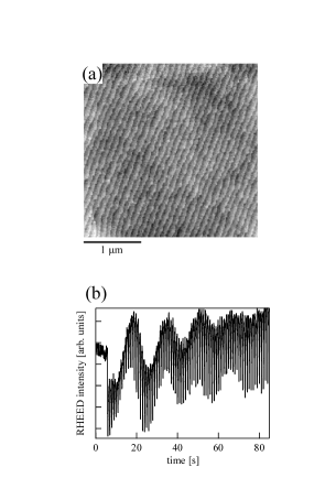
Epitaxial Nb-STO films were fabricated on (001) SrTiO3 (STO) single crystal substrates. Pulsed laser deposition (PLD) employing KrF excimer laser pulses (0.5 J/cm2, 1 Hz) focused on a single crystal 1wt% (2atom%) Nb-STO target and very high substrate temperatures were used. In order to reach the required high substrate temperature of up to 1300, an infrared (807 nm) diode laser was used, illuminating the substrate from outside of the UHV chamber through a view port S. Ohashi . During the deposition, reflection high-energy electron diffraction (RHEED) patterns and specular spot intensities were monitored in situ. The substrate temperature was kept at 12001300 under an oxygen pressure of 2 Torr. After the deposition, the films were cooled down to 500 and kept in 760 Torr of oxygen for 1 hour to re-oxidize both the substrate and the film. Figure 1 (a) shows an atomic force microscope (AFM) topographic image of a Nb-STO film, 500 Å thick. The scan area is 33m2. No particles were observed and the straight lines correspond to the 3.9 Å height perovskite unit cell steps. Figure 1 (b) shows the specular intensity of a RHEED reflection as a function of time during the deposition. As can be seen in the Figure, long period (20 s) oscillations and quick recovery, just after each laser pulse, were observed. The thickness measurements after the deposition revealed that the long period corresponds to one perovskite unit cell growth. This result indicates that the growth mode is “between” the layer-by-layer and the step flow growth modes M. Lippmaa . The 2-dimensional growth mode is consistent with the flat surfaces measured in AFM topography images as shown in Fig. 1 (a). Though x-ray diffraction measurements were performed, no film peak could be detected, the strong substrate peaks very likely masking the film reflections, suggesting that the lattice constant of the films is essentially identical to that of the substrate (3.905 Å).
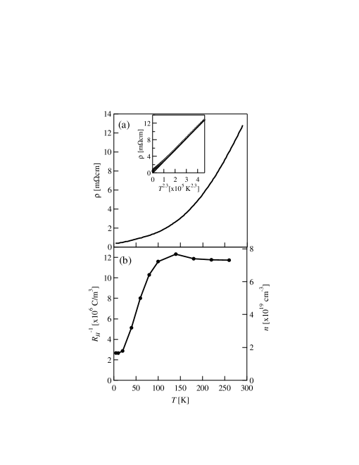
To perform detailed transport measurements, photolithography and wet etching were used to define a conducting path allowing resistivity and Hall effect to be measured. The current path width was 60 m and the distance between the voltage electrodes 100 m. The film thickness of the sample investigated here is about 260 Å.111The measured film was covered by a PZT layer used for ferroelectric field effect experiments. Figure 2 (a) shows the temperature dependence of the resistivity. The room temperature resistivity is about 13 mcm. Lowering the temperature, one observes a large decrease of the resistivity, similar to what has been observed in doped STO single crystals O. N. Tufte . The residual resistivity is 500 cm and the residual resistivity ratio about 26. This low temperature resistivity value is a record low value for thin films in this doping range. The lowest low temperature resistivity of Nb-doped single crystal reported is however one order of magnitude smaller, reaching about 60 cm O. N. Tufte . Though analysis of the temperature dependence of resistivity was performed, no simple transport mechanism could be identified. In single crystals a power low , independent of the doping level, was reported between 150 and 300 K O. N. Tufte . Here, as shown in the inset of Figure 2(a), the resistivity versus temperature is well described in the same temperature range by , however, the 2.3 exponent cannot be simply related to any scattering mechanism and further investigations will be necessary to understand transport and the remarkable metallicity observed in this system. Also, it is quite probable, in view of the different low temperature resistivity values measured from film to film, that some structural differences or defects, e.g. epitaxial lattice strain, may affect both the resistivity value at low temperature and the temperature dependence of the resistivity. Figure 2 (b) shows the temperature dependence of the inverse Hall coefficient (). As can be seen in the Figure, above 100 K the inverse Hall constant is essentially temperature independent (as one would expect for a simple metal). However, below 100 K, a dramatic decrease of the Hall constant is observed with a low temperature value being a factor of 4 smaller than the high temperature value. This behavior is very different from the essentially temperature independent Hall constant observed in single crystals O. N. Tufte . The origin of the large decrease of at low temperatures is still to be understood in detail. It could be related to the existence of two types of carriers in doped STO as documented in several papers L. F. Mattheiss_1 ; G. Binning . As suggested by recent ferroelectric field effect experiments, extracting the carrier density from the value using the simple relation = is only possible above 100 K K. S. Takahashi-2 . Using the high temperature value, = C/m3 , one obtains a carrier density of cm-3. The ratio between the Nb doping and the active Nb donors would then only be 22%, which is less than previously reported (50 %) for thin films A. Leitner and single crystals H. P. R. Frederikse ; C. Lee .
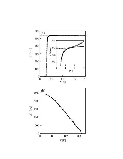
Below 4.2 K, a dilution refrigerator was used to perform transport measurements down to 50 mK. As shown in Fig. 3 (a), the film shows a superconducting transition around 0.3 K and the resistivity drops to zero at about 0.25 K. We observe that the resistivity starts to deviate from its normal state behavior below about 1.4 K as shown in the inset. As shown by the solid line, a 2-dimensional (2D) superconducting fluctuation model ()2D model allows a good fit to the curve from 1.4 K to just above Tc. Superconductivity is suppressed by applying a magnetic field along the [001] direction (out of the film plane). Figure 3 (b) shows the upper critical field () as a function of T defined as the temperature at which the resistivity reaches 90% of the normal state value (taken at 400mK). The temperature dependence can be roughly fitted to the WHH model that describes conventional dirty limit type-II superconductors N. R. Werthamer . The coherence length at 0 K can be obtained from the extrapolated zero temperature value of and is about 360 Å (using Hc2(0) = ). The fact that the coherence length is larger than the film thickness 260 Å indicates that the system is a 2D superconductor. This is consistent with the fact that the paraconductivity observed above Tc can be explained by 2D superconducting fluctuations. Finally, Fig. 4 shows the Tc vs carrier density for oxygen reduced and Nb doped single crystals adapted from references E. R. Pfeiffer ; C. S. Koonce . Using the measured Tc value and the carrier density extracted using the high temperature Hall effect measurements, one can position our thin film on this graph. As can be seen, the film falls between the two bulk Tc versus curves. The reason for the Tc difference between reduced and Nb-doped single crystals is as yet unknown. It should also be noted that if the system is a 2D superconductor, one expects a Kosterlitz-Thouless (K-T) transition with a K-T transition temperature proportional to the superfluid density (at TKT) J. M. Kosterlitz . This should manifest itself in the tail of the transition and more experiments will be necessary to precisely determine the exact role played by 2D fluctuations.

III CONCLUSION
In conclusion, we have fabricated (001) Nb-doped SrTiO3 epitaxial thin films by pulsed laser deposition. Laser heating provided high substrate temperatures which allowed a 2-dimensional growth to be obtained, as confirmed by RHEED and AFM measurements. Transport measurements reveal a metallic behavior with a low residual resistivity and a sharp superconducting transition. Because of the large coherence length, 2D superconducting fluctuations are expected and observed close to the superconducting transition. Such high quality superconducting films might be useful in bringing the realization of superconducting field effect devices a step closer.
Acknowledgements
The authors would like to thank Matthew Dawber for a careful reading of the manuscript. This work was supported by the Swiss National Science Foundation through the National Center of Competence in Research, “Materials with Novel Electronic Properties, MaNEP” and division II, New Energy and Industrial Technology Development Organization (NEDO) of Japan, and ESF (Thiox).
References
- (1) J. F. Schooley, W. R. Hosler, and M. L. Cohen, “Superconductivity in semiconducting SrTiO3,” Phys. Rev. Lett. 12, pp. 474–475, 1964.
- (2) E. R. Pfeiffer and J. F. Schooley, “Superconducting transition temperatures of Nb-doped SrTiO3,” Phys. Lett. 29A, pp. 589–590, 1969.
- (3) C. S. Koonce, M. L. Cohen, J. F. Schooley, W. R. Hosler, and E. R. Pfeiffer, “Superconducting transition temperatures of semiconducting SrTiO3,” Phys. Rev. 163, pp. 380–390, 1967.
- (4) See, for instance, the recent review by C. H. Ahn, J. -M. Triscone, and J. Mannhart, “Electric field effect in correlated oxide systems,” Nature 424, pp. 1015–1018, 2003.
- (5) K. L. Myers, Ph.D. thesis, Stanford University, 1993.
- (6) O. N. Tufte and P. W. Chapman, “Electron mobility in semiconducting strontium titanate,” Phys. Rev. 155, pp. 796–802, 1967.
- (7) A. Leitner, C. T. Rogers, J. C. Price, D. A. Rudman, D. R. Herman, “Pulsed laser deposition of superconducting Nb-doped strontium titanate thin films,” Appl. Phys. Lett. 72, pp. 3065–3067, 1998.
- (8) A. Leitner, D. Olaya, C. T. Rogers, and J. C. Price, “Upper critical field and fluctuation conductivity in Nb-doped strontium titanate thin films,” Phys. Rev. B 62, pp. 1408–1413, 2000.
- (9) D. Olaya, F. Pan, C. T. Rogers, and J. C. Price, “Superconductivity in La-doped strontium titanate thin films,” Appl. Phys. Lett. 84, pp. 4020–4022, 2004.
- (10) K. S. Takahashi, D. Matthey, D. Jaccard, J.-M. Triscone, K. Shibuya, T. Ohnishi, and M. Lippmaa, “Electrostatic modulation of the electronic properties of Nb-doped SrTiO3 superconducting films,” Appl. Phys. Lett. 84, pp. 1722–1724, 2004.
- (11) S. Ohashi, M. Lippmaa, N. Nakagawa, H. Nagasawa, H. Koinuma, and M. Kawasaki, “Compact laser molecular beam epitaxy system using laser heating of substrate for oxide film growth,” Rev. Sci. Instrum. 70, pp. 178–183, 1999.
- (12) M. Lippmaa, N. Nakagawa, M. Kawasaki, S. Ohashi, and H. Koinuma, “Growth mode mapping of SrTiO3 epitaxy,” Appl. Phys. Lett. 76, pp. 2439–2441, 2000.
- (13) L. F. Mattheiss, “Energy bands for KNiF3, SrTiO3, KMoO3, and KTaO3,” Phys. Rev. B 6, pp. 4718–4740, 1972.
- (14) G. Binning, A. Baratoff, H. E. Hoenig, and J. G. Bednorz, “Two-band superconductivity in Nb-doped SrTiO3,” Phys. Rev. Lett. 45, pp. 1352–1355, 1980.
- (15) K. S. Takahashi et al., in preparation.
- (16) H. P. R. Frederikse and W. R. Hosler, “Hall mobility in SrTiO3,” Phys. Rev. 161, pp. 822–827, 1967.
- (17) C. Lee, J. Destry, and J. L. Brebner, “Optical absorption and transport in semiconducting SrTiO3,” Phys. Rev. B 11, pp. 2299–2310, 1975.
- (18) M. Tinkham, Introduction to superconductivity. 2nd ed. ,McGraw-Hill, New York, 1996.
- (19) N. R. Werthamer, E. Helfand, and P. C. Hohenberg, “Temperature and purity dependence of the superconducting critical field, . III. Electron spin and spin-orbit effects,” Phys. Rev. 147, pp. 295–302, 1966.
- (20) J. M. Kosterlitz and D. J. Thouless, “Long range order and metastability in two dimensional solids and superfluids,” J. Phys. C: Solid State Phys. 5, pp. L124–L126, 1972.