Localization Transition in a Ballistic Quantum Wire
Abstract
The many-body wave-function of an interacting one-dimensional electron system is probed, focusing on the low-density, strong interaction regime. The properties of the wave-function are determined using tunneling between two long, clean, parallel quantum wires in a GaAs/AlGaAs heterostructure, allowing for gate-controlled electron density. As electron density is lowered to a critical value the many-body state abruptly changes from an extended state with a well-defined momentum to a localized state with a wide range of momentum components. The signature of the localized states appears as discrete tunneling features at resonant gate-voltages, corresponding to the depletion of single electrons and showing Coulomb-blockade behavior. Typically such features appear, where the one-electron state has a single-lobed momentum distribution, and the few-electron states have double-lobed distributions with peaks at . A theoretical model suggests that for a small number of particles (), the observed state is a mixture of ground and thermally excited spin states.
pacs:
73.21.Hb,73.20.Qt,73.23.AdCoulomb interactions in many-body quantum systems can lead to the creation of exotic phases of matter. A prime example is a Luttinger liquid, which describes a system of interacting electrons confined to one spatial dimension Haldane (1981). At high electron densities the electron kinetic energy dominates over the Coulomb energy and the transport properties of the system resemble those of non-interacting electrons. In this weakly interacting limit, conductance is quantized even in the presence of moderate disorder Tarucha et al. (1995); Yacoby et al. (1996). Reducing the electron density suppresses the kinetic energy more rapidly than the Coulomb energy, leading to the strongly interacting limit, where charge correlations resemble those in a Wigner crystal, an ordered lattice of electrons with periodicity (, the mean electron density). In this limit, one expects the weakest amount of disorder to pin the crystal, thereby suppressing conductance at low temperatures Glazman et al. (1992). Here we investigate the suppression of conductance and the changes in the electron wavefunction as is reduced, using momentum-resolved tunneling. We find a remarkably sharp localization transition at low densities.
Momentum resolved tunneling between two quantum wires has been shown to be an effective experimental tool in the study of interacting one-dimensional (1D) systems. This method uses tunneling across an extended junction between two closely situated parallel clean quantum wires Auslaender et al. (2002). An electron tunneling across the junction transfers momentum ( is the magnetic field perpendicular to the plane of the wires, is the distance between them, as in Fig. 1). When the source drain bias voltage applied across the junction is low, the probability for an electron to tunnel between the wires can be measured through the low-bias tunneling conductance Auslaender et al. (2005). At low temperatures , assuming the lower wire is uniform and weakly interacting, where is the tunneling matrix element. is given by
| (1) |
where is a “quasi-wavefunction” for the upper wire, defined by: . Here , are the Fermi-wavenumbers in the Upper, Lower wires (UW, LW), is the ground state for particles in the UW, and is an operator that removes an electron from point in the UW Fiete et al. . At finite temperatures, several states contribute, and the conductance is proportional to a weighted average of their corresponding . In the absence of interactions, would be the wave function of the th electron, which is a plane-wave for an infinite system. In this case we intuitively expect . is therefore finite only when , with
| (2) |
allowing tunneling only between the Fermi-points of the two wires.
The precise line shape of encodes details of the microscopic properties of the many-body states involved in the tunneling process: A realistic, finite size junction introduces effects manifest as fringes accompanying the -function peaks of Tserkovnyak et al. (2002). Electron-electron interactions reduce the norm of , but many of its qualitative features remain unchanged for clean, long wires at low temperatures: should have peaks at the same values of as in the non-interacting case. We use to probe the real-space structure of in the presence of confinement and electron interactions. We report on measurements of as a function of , following it down to the strongly interacting, low-density regime.
The experimental setup is schematically drawn in Fig. 1. It is realized by two parallel wires at the edges of two quantum wells fabricated in a GaAs/AlGaAs heterostructure by cleaved edge overgrowth (CEO) Pfeiffer et al. (1993). Only the top quantum well ( deep) is populated by a two-dimensional electron gas (2DEG) which serves as a contact to the UW through ohmic contacts . The experiment is set up using -wide tungsten gates on the top surface : is set to a negative voltage where the UW is depleted and LW remains continuous, so that only the tunneling current is measured between source and drain . is set to deplete both wires, so that the tunneling junction at the drain is much longer than the one at the source, ensuring that the LW is kept at drain potential. The density of a segment in the wire is varied by applying voltage to . is set to drain voltage to allow simultaneous reading of 2-terminal UW conductance and tunneling conductance. The density-dependent measurement consists of setting and measuring the tunneling current as a function of . The tunneling current includes contributions which are not dependent. To single out the density-dependent contribution, the differential tunneling conductance is measured using a lock-in. Typically is a few with a frequency. The measurements are performed in a refrigerator at temperatures down to .
Initially a cooled sample has one populated sub-band in the UW (henceforth “single-mode wire”). The potential landscape along the UW is marked by in Fig. 1, where the depletion of the wire requires a relatively small negative gate voltage (). Illuminating the sample with infrared light increases the electron density in the wire thus allowing further population of higher sub-bands (“multi-mode wire”). Depletion of the wire after illumination requires a larger () gate voltage. The finite slope in results in a shorter effective length of the low-density region.
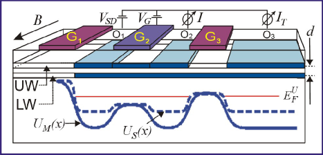
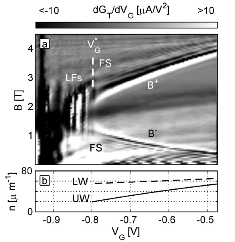
Fig. 2 (a) shows the measurement of for a single-mode wire. The figure is dominated by a set of curves marked . The upper curve corresponds to sign in Eq. 2 and is the measured differential conductance which results from tunneling between counter-propagating states. The lower curve corresponds to the sign in Eq. 2 which in turn results from tunneling between co-propagating states. Each curve is accompanied by Finite Size fringes (FS) which are a consequence of the finite length of the low-density region. As the top-gate voltage grows more negative the density under the gate is reduced and the curves converge. Panel (b) shows the densities in both wires as extracted using Eq. 2.
An abrupt change in is evident in Fig. 2 at a critical gate-voltage , which corresponds to a critical UW density . At the high density features disappear, giving way to a different set of features labelled Localization Features (LFs). This is a fundamental change: When the wire is uniform and momentum is a good quantum number. is therefore appreciable only in a narrow range of around , being the length of the density-tuned region. When The momentum range spanned by the LFs is typically very broad and lies roughly between the extrapolations of the curves. Further attesting to the importance of this transition, we note that simultaneous reading of and (Fig. 1) shows that this change is concurrent with the suppression of the 2-terminal conductance Auslaender et al. (2005).
The broad momentum spectrum exhibited by the LFs may have several possible interpretations. For example, may be localized on a length scale not much larger than the inter-particle separation. Alternatively, broad LFs may result either from non-uniform density which gives way to a broad distribution of local Fermi wavevectors, or from contributions of states above the ground state, with excitations that soak up part of the transferred momentum.
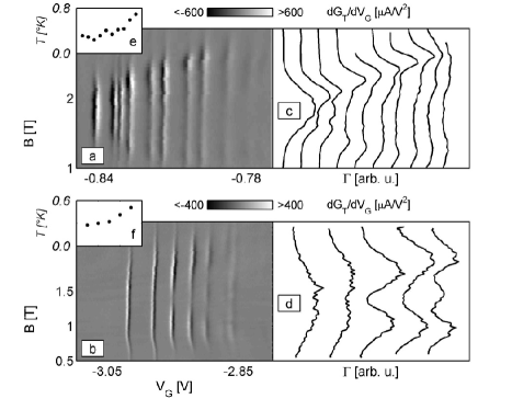
The LFs are studied more closely in Fig. 3 where high-resolution scans of single-mode and multi-mode wire LFs are presented (panels (a) and (b) respectively). The LFs appear as vertical streaks in . They are narrow in the direction, separated by strips with vanishing signal. Such discrete behavior is a result of charge quantization typical of Coulomb blockade (CB) of electrons in a finite box. The number of the LFs for several cases is summarized in Table 1.
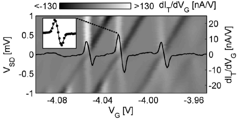
The CB behavior, along with the observation that the UW states are localized, implies the existence of a localized region separated from the rest of the UW by tunnel-barriers. This localized region forms a quantum-dot with three leads: Two leads are the UW segments which are not density controlled, and one is the LW. It is not clear, however, why in this regime we typically don’t detect resonances in the UW conductance. As expected from CB physics, when a finite source-drain bias is applied (Fig. 4), the LFs split to form the well known diamonds Grabert and Devoret (1992). The asymmetry of the diamonds indicates different capacitance to each lead.
We define the length of the low-density region above and below as and respectively. Both are extracted from the data: In the extended regime, , finite size fringes accompany the curves for values of and , (marked by “FS” in Fig. 2). The location of the FS, outside the curves, implies that the electron density here has a minimum in the center of the UW, with a length , being the spacing of the fringes in the direction Tserkovnyak et al. (2002). In the localized regime, , , where is the number of electrons confined to the low-density region (number of LFs). Table 1 summarizes the results for the LFs presented in this paper and in Auslaender et al. (2005). We see that . This suggests that the entire low-density region participates in the localization.
| Sub-band: | |||||
|---|---|---|---|---|---|
| Single-Mode | 12 | 20 | 0.6 | 1.0 | -0.9 |
| Multi-Mode 2nd | 5 | 22 | 0.23 | -2.6 | |
| Multi-Mode 1st | 6 | 25 | 0.24 | 0.5 | -3.6 |
Fig. 4 contains a line-scan showing the cross section of the peaks and a fit to a second derivative of the Fermi-function, using two adjustable parameters: The width of the peak, scaling linearly with temperature, and its height, which is proportional to the tunneling rate, . Such fits were performed for each value of in Fig. 3. The extracted values of are presented in Fig. 3(c) and (d). The Coulomb-blockaded states can now be characterized by , which is a direct measure of their momentum distribution (Using Eqs. 1 and 2). The single-mode measurement presented in panel (c) shows a generic case where has a single peak for the first LF and two broad peaks for , with a separation that increases as N is increased. There is only little variation in this behavior upon different cool-downs, single vs. multi-mode conditions and when a different gate is used. Rarely one can find momentum distribution that can be interpreted using single particle theory. Fig. 3(d) shows the LF’s of subband 2 in a multi mode wire. One can clearly see that are approximately single-lobed, double-lobed, and is triple lobed. This behavior is characteristic of the the three first spin degenerate wave function in a one dimensional well Fiete et al. .
Insets (e) and (f) of Fig. 3 show the medians of the temperature fit for each of the LFs in (a) and (b) respectively. The temperature is originally obtained in units of and is translated to using the capacitance ratio measured in scans such as Fig. 4. The deduced temperature appears to increase with the addition of electrons, almost by a factor of . The apparent broadening of the feature can not be explained by level broadening since the line-shape does not resemble a Lorentzian. Furthermore, scans such as Fig. 4 rule out the possibility that the features broaden due to changing of lead-dot capacitance. We currently do not have a straightforward explanation for this observation.
In an attempt to model the data, we have calculated the expected tunneling form factor in the localized regime: For , has no nodes. This agrees with the experimental results in Fig. 3 (b) and (d). For , however, where the spin-singlet ground state would reproduce a similar signature, the observed deviates from the single-lobe structure. We therefore estimate the energy difference between the lowest triplet state and the singlet ground state for the two electron system and find it to be extremely small, less than the Zeeman energy in a field of . Mixing of the singlet-triplet states at finite temperatures reproduces the observed structure: A pair of maxima at finite with a non-zero local minimum at Fiete et al. .
The energy scale for spin-excitations grows rapidly with increasing density, and at we expect spin excitations to be frozen out for . The estimate is sensitive to the form and size of the cutoff in the interaction potential. Calculations assuming sharp confinement lead to a form factor which becomes sharply peaked near . The broad peaks observed experimentally and the substantial weight near could be a result of softness or asymmetry in the confining potential, some residual disorder, or thermally excited spin-excitations (possibly due to the exchange energy being smaller than our estimate) Cheianov and Zvonarev (2004); Fiete and Balents (2004); Fiete et al. .
In conclusion, we have studied the momentum-structure of the many-body wave-function of an interacting quantum-wire. We find that below the critical density , where the 2-terminal conductance is suppressed, the electrons are bound to a localized region and display Coulomb-blockade charging physics. Momentum spectroscopy of the localized few-electron states reveals an evolution of momentum structure from single-peak to double-peak.
We would like to thank R. de-Picciotto for his contribution. Y. Oreg and T. Giamarchi assisted in helpful discussions. This work was supported in part by the US-Israel BSF, the European Commission RTN Network Contract No. HPRN-CT-2000-00125 and NSF grants DMR-02-33773 and PHY-01-17795. YT is supported by the Harvard Society of Fellows. GAF is supported by NSF grant PHY-99-07949 and by the Packard Foundation. OMA acknowledges partial support from a grant from the Israeli Ministry of Science. HS is supported by a grant from the Israeli Ministry of Science.
Present address: Gaballe Laboratory for Advanced Materials, Stanford University, Stanford, CA 94305, USA.
References
- Haldane (1981) F. D. M. Haldane, J. Phys. C 14, 2585 (1981).
- Tarucha et al. (1995) S. Tarucha, T. Honda, and T. Saku, Solid State Comm. 94, 413 (1995).
- Yacoby et al. (1996) A. Yacoby, H. L. Stormer, N. S. Wingreen, L. N. Pfeiffer, K. W. Baldwin, and K. W. West, Phys. Rev. Lett. 77, 4612 (1996).
- Glazman et al. (1992) L. I. Glazman, I. M. Ruzin, and B. I. Shklovskii, Phys. Rev. B 45, 8454 (1992).
- Auslaender et al. (2002) O. M. Auslaender, A. Yacoby, R. de Picciotto, K. W. Baldwin, L. N. Pfeiffer, and K. W. West, Science 295, 825 (2002).
- Auslaender et al. (2005) O. M. Auslaender, H. Steinberg, A. Yacoby, Y. Tserkovnyak, B. I. Halperin, K. W. Baldwin, L. N. Pfeiffer, and K. W. West, Science 308, 88 (2005).
- (7) G. A. Fiete, J. Qian, Y. Tserkovnyak, and B. I. Halperin, cont-mat/0501684.
- Tserkovnyak et al. (2002) Y. Tserkovnyak, B. I. Halperin, O. M. Auslaender, and A. Yacoby, Phys. Rev. Lett. 89, 136805 (2002).
- Pfeiffer et al. (1993) L. N. Pfeiffer, H. L. Stormer, K. W. Baldwin, K. W. West, A. R. Goñi, A. Pinczuk, R. C. Ashoori, M. M. Dignam, and W. Wegscheider, J. Crystal Growth 127, 849 (1993).
- Tserkovnyak et al. (2003) Y. Tserkovnyak, B. I. Halperin, O. M. Auslaender, and A. Yacoby, Phys. Rev. B 68, 125312 (2003).
- Grabert and Devoret (1992) H. Grabert and M. H. Devoret, eds., Single Charge Tunneling: Coulomb Blockade Phenomena in Nanostructures (NATO ASI Ser. B.), vol. 294 (Plenum Press, New York, 1992).
- Cheianov and Zvonarev (2004) V. Cheianov and M. Zvonarev, Phys. Rev. Lett. 92, 176401 (2004).
- Fiete and Balents (2004) G. A. Fiete and L. Balents, Phys. Rev. Lett. 93, 226401 (2004).